 | –≠–ª–µ–∫—Ç—Ä–æ–Ω–Ω—ã–π –∫–æ–º–ø–æ–Ω–µ–Ω—Ç: W26L010 | –°–∫–∞—á–∞—Ç—å:  PDF PDF  ZIP ZIP |
W26L010A
64K
◊
16 HIGH-SPEED CMOS STATIC RAM
Publication Release Date: July 1998
- 1 -
Revision A3
GENERAL DESCRIPTION
The W26L010A is a high-speed, low-power CMOS static RAM organized as 65,536
◊
16 bits that
operates on a single 3.3-volt power supply. This device is manufactured using Winbond's high
performance CMOS technology.
The W26L010A has an active low chip select, separate upper and lower byte selects, and a fast
output enable. No clock or refreshing is required. Separate byte select controls (
LB
and UB ) allow
individual bytes to be written and read.
LB
controls I/O1-I/O8, the lower byte. UB controls I/O9
-
I/O16, the upper byte. This device is well suited for use in high-density, high-speed system
applications.
FEATURES
∑
High speed access time: 10/12 nS (max.)
∑
Low power consumption:
-
Active: 530 mW (max.)
∑
Single
+
3.3V power supply
∑
Fully static operation
-
No clock or refreshing
∑
All inputs and outputs directly TTL compatible
∑
Three-state outputs
∑
Data byte control
-
LB
(I/O1
-
I/O8),
UB
(I/O9
-
I/O16)
∑
Available packages: 44-pin 400 mil SOJ and
44-pin TSOP(II)
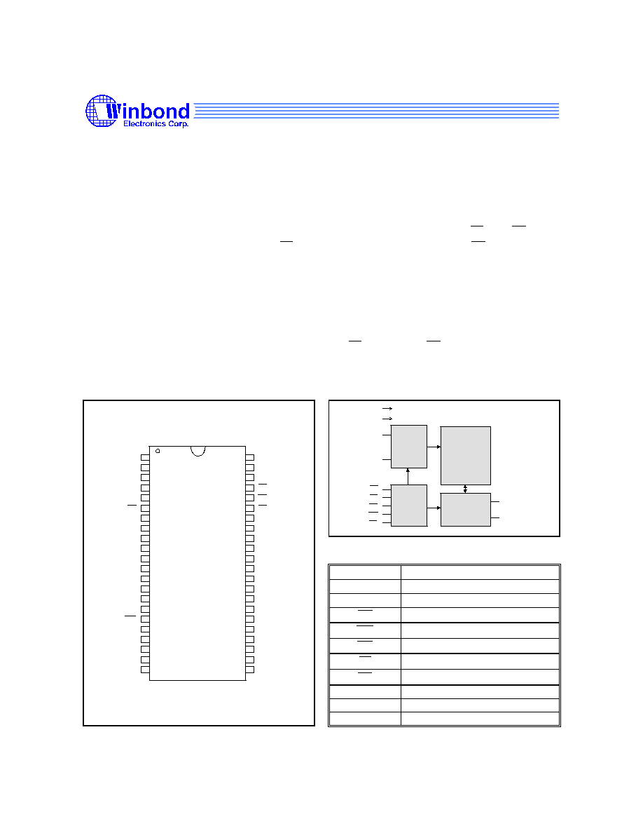
PIN CONFIGURATION
1
2
3
4
5
6
7
8
9
10
11
12
13
14
15
16
17
18
19
20
21
22
44
43
42
41
40
39
38
37
36
35
34
33
32
31
30
29
28
27
26
25
24
23
A0
A1
A2
A3
A4
CS
I/O1
I/O2
I/O3
I/O4
V
DD
V
SS
I/O5
I/O6
I/O7
I/O8
WE
A5
A6
A7
A8
NC
NC
A9
A10
A11
A12
NC
I/O9
I/O10
I/O11
I/O12
V
DD
V
SS
I/O13
I/O14
I/O15
I/O16
LB
UB
OE
A13
A14
A15
44-PIN
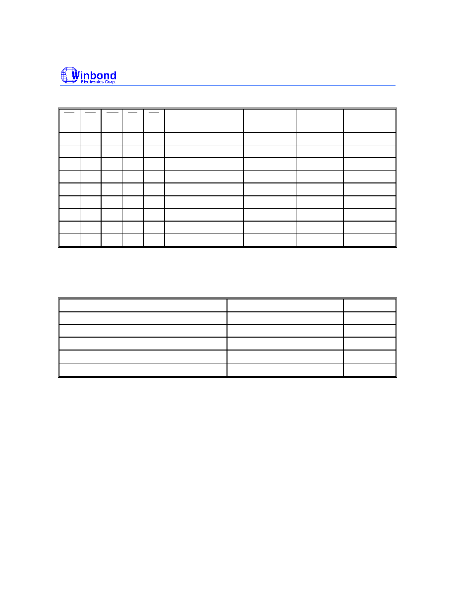
BLOCK DIAGRAM
A0
.
.
A15
I/O1
I/O16
V
DD
V
SS
.
.
DATA I/O
DECODER
CONTROL
UB
CS
OE
WE
LB
CORE
ARRAY
PIN DESCRIPTION
SYMBOL
DESCRIPTION
A0
-
A15
Address Inputs
I/O1
-
I/O16
Data Inputs/Outputs
CS
Chip Select Inputs
WE
Write Enable Input
OE
Output Enable Input
LB
Lower Byte Select I/O1
-
I/O8
UB
Upper Byte Select I/O9
-
I/O16
V
DD
Power Supply
V
SS
Ground
NC
No Connection
W26L010A
- 2 -
TRUTH TABLE
CS
OE
WE
LB
UB
MODE
I/O1
-
I/O8
I/O9
-
I/O16
V
DD
CURRENT
H
X
X
X
X
Not Selected
High Z
High Z
I
SB
, I
SB1
L
H
H
X
X
Output Disable
High Z
High Z
I
DD
L
L
H
L
L
2 Bytes Read
D
OUT
D
OUT
I
DD
L
L
H
L
H
Lower Byte Read
D
OUT
High Z
I
DD
L
L
H
H
L
Upper Byte Read
High Z
D
OUT
I
DD
L
X
L
L
L
2 Bytes Write
D
IN
D
IN
I
DD
L
X
L
L
H
Lower Byte Write
D
IN
High Z
I
DD
L
X
L
H
L
Upper Byte Write
High Z
D
IN
I
DD
L
X
X
H
H
Output Disable
High Z
High Z
I
DD
DC CHARACTERISTICS
Absolute Maximum Ratings
PARAMETER
RATING
UNIT
Supply Voltage to V
SS
Potential
-0.5 to +4.6
V
Input/Output to V
SS
Potential
-0.5 to V
DD
+0.5
V
Allowable Power Dissipation
1.5
W
Storage Temperature
-65 to +150
∞
C
Operating Temperature
0 to +70
∞
C
Note: Exposure to conditions beyond those listed under Absolute Maximum Ratings may adversely affect the life and reliability of the
device.

W26L010A
Publication Release Date: July 1998
- 3 -
Revision A3
Operating Characteristics
(V
DD
= 3.3V
±
5%, V
SS
= 0V, T
A
= 0 to 70
∞
C)
PARAMETER
SYM.
TEST CONDITIONS
MIN.
TYP. MAX. UNIT
Input Low Voltage
V
IL
-
-0.5
-
+0.8
V
Input High Voltage
V
IH
-
+2.0
-
V
DD
+0.3
V
Input Leakage
Current
I
LI
V
IN
= V
SS
to V
DD
-10
-
+10
µ
A
Output Leakage
Current
I
LO
V
I/O
= V
SS
to V
DD
Output Pins in High Z,
See Truth Table
-10
-
+10
µ
A
Output Low Voltage
V
OL
I
OL
= +8.0 mA
-
-
0.4
V
Output High Voltage
V
OH
I
OH
= -4.0 mA
2.4
-
-
V
Operating Power
I
DD
CS = V
IL
(max.), Cycle =
min.
10
-
-
160
mA
Supply Current
I/O = open, Duty = 100%
12
-
-
140
Standby Power
I
SB
CS = V
IH
(min.), Cycle = min.
-
-
30
mA
Supply Current
I
SB1
CS = V
DD
-0.2V, I/O = open
All other pins = V
DD
-0.2V/GND
-
-
10
mA
Note: Typical characteristics are evaluated at V
DD
= 3.3V, T
A
= 25
∞
C.
CAPACITANCE
(V
DD
= 3.3V, T
A
= 25
∞
C, f = 1 MHz)
PARAMETER
SYM.
CONDITIONS
MAX.
UNIT
Input Capacitance
C
IN
V
IN
= 0V
6
pF
Input/Output Capacitance
C
I/O
V
OUT
= 0V
8
pF
Note: These parameters are sampled but not 100% tested.
AC CHARACTERISTICS
AC Test Conditions
PARAMETER
CONDITIONS
Input Pulse Levels
0V to 3V
Input Rise and Fall Times
2 nS
Input and Output Timing Reference Level
1.5V
Output Load
C
L
= 30 pF, I
OH
/I
OL
= -4 mA/8 mA

W26L010A
- 4 -
AC Test Loads and Waveform
R1 320 ohm
3.3V
OUTPUT
R2
350 ohm
5 pF
R2
350 ohm
R1 320 ohm
3.3V
OUTPUT
30 pF
Including
Jig and
Scope
90%
90%
2 nS
10%
2 nS
10%
3.0V
0V
Including
Jig and
Scope
)
( For T
T
T
OLZ,
T
T
WHZ,
T
OW
T
CLZ,
BLZ,
CHZ,
BHZ,
T
OHZ,
(V
DD
= 3.3V
±
5%, V
SS
= 0V, T
A
= 0 to 70
∞
C)
(1) Read Cycle
PARAMETER
SYM.
W26L010A-10
W26L010A-12
UNIT
MIN.
MAX.
MIN.
MAX.
Read Cycle Time
T
RC
10
-
12
-
nS
Address Access Time
T
AA
-
10
-
12
nS
Chip Select Access Time
T
ACS
-
10
-
12
nS
Output Enable to Output Valid
T
OE
-
5
-
6
nS
UB , LB Access Time
T
BA
-
5
-
6
nS
Output Hold from Address Change
T
OH
3
-
3
-
nS
Chip Select to Output in Low Z
T
CLZ*
3
-
3
-
nS
Chip Deselect to Output in High Z
T
CHZ*
-
5
-
6
nS
Output Enable to Output in Low Z
T
OLZ*
0
-
0
-
nS
Output Disable to Output in High Z
T
OHZ
*
-
5
-
6
nS
UB , LB Select to Output in Low Z
T
BLZ*
0
-
0
-
nS
UB
,
LB
Deselect to Output in High Z
T
BHZ*
-
5
-
6
nS
These parameters are sampled but not 100% tested.

W26L010A
Publication Release Date: July 1998
- 5 -
Revision A3
AC Characteristics, continued
(2) Write Cycle
PARAMETER
SYM.
W26L010A-10
W26L010A-12
UNIT
MIN.
MAX.
MIN.
MAX.
Write Cycle Time
T
WC
10
-
12
-
nS
Chip Select to End of Write
T
CW
9
-
10
-
nS
Address Valid to End of Write
T
AW
9
-
10
-
nS
Address Setup Time
T
AS
0
-
0
-
nS
UB , LB Select to End of Write
T
BW
9
-
10
-
nS
Write Pulse Width
T
WP
9
-
10
-
nS
Write Recovery Time
CS , WE
T
WR
0
-
0
-
nS
Data Valid to End of Write
T
DW
6
-
7
-
nS
Data Hold from End of Write
T
DH
0
-
0
-
nS
Write to Output in High Z
T
WHZ*
-
6
-
7
nS
End of Write to Output Active
T
OW*
3
-
3
-
nS
These parameters are sampled but not 100% tested.

W26L010A
- 6 -
Timing Waveforms
Read Cycle 1
(Address Controlled,
CS
=
OE
=
UB
=
LB
= V
IL
,
WE
= V
IH
)
Address
T
T
T
T
D
OH
AA
RC
OH
OUT
Read Cycle 2
(Chip Select Controlled,
OE
= V
IL
,
WE
= V
IH
)
Address
RC
T
T
ACS
T
CS
CHZ
T
CLZ
D
T
BLZ
OUT
UB / LB
T
BHZ
T
OE
OHZ
T
OLZ
T
BA
T
OE
HIGH-Z
HIGH-Z
Notes:
1. WE is high for read cycle.
2. Device is continuously selected.
CS
= OE = LB = Low
CS
= OE = LB = Low
3. Address valid prior to or coincident with CS
transition low.

W26L010A
Publication Release Date: July 1998
- 7 -
Revision A3
Timing Waveforms, continued
Read Cycle 3
(Output Enable Controlled,
CS
=
UB
=
LB
= V
IL
,
WE
= V
IH
)
Address
T
T
T
T
OE
OH
AA
RC
AOE
D
OUT
T
OLZ
T
OHZ
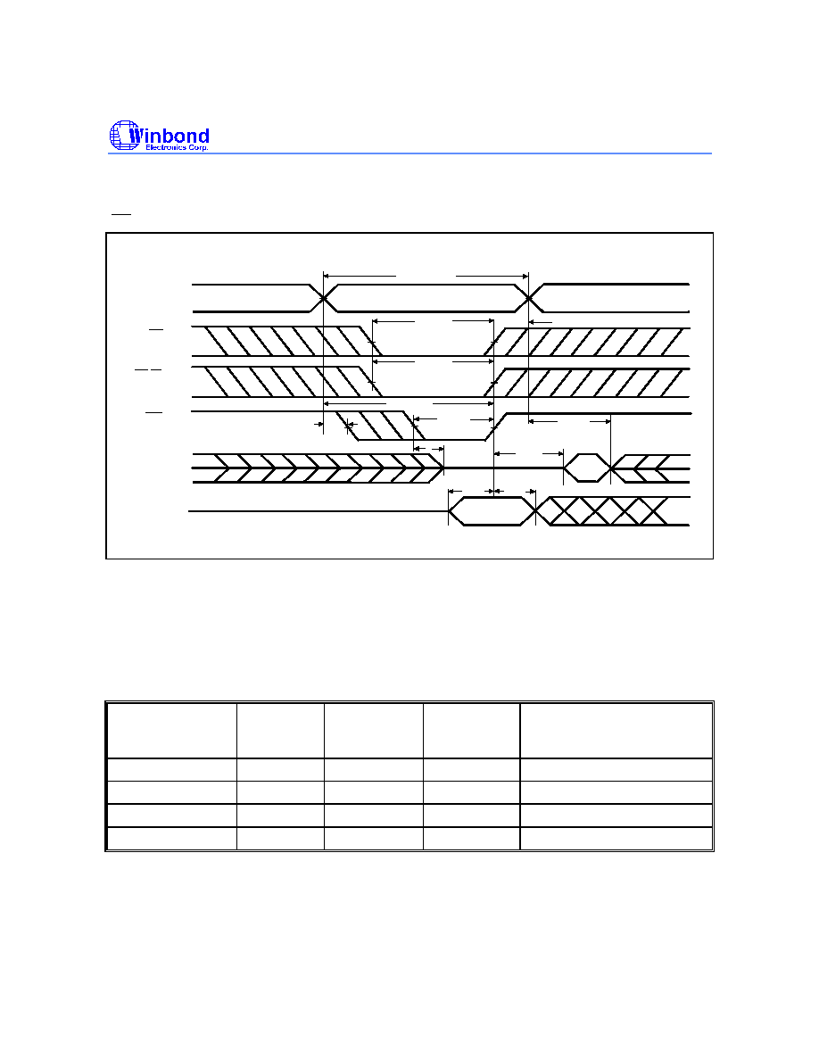
Write Cycle 1
(OE Clock)
Address
OE
WE
D
D
T
OUT
IN
WC
T
WR
T
T
AW
T
WP
T
AS
T
DW
T
DH
CS
CW
BW
T
UB/LB
W26L010A
- 8 -
Timing Waveforms, continued
Write Cycle 2
(OE = V
IL
Fixed)
Address
WE
D
D
T
T
T
T
T
T
T
(2)
(3)
T
T
WC
AW
WP
OW
WHZ (1, 4)
DW
DH
OH
AS
OUT
IN
CS
T
T
CW
WR
UB/LB
T
BW
Notes:
1. During this period, I/O pins are in the output state, so input signals of opposite phase to the outputs should not be applied.
2. The data output from D
OUT
are the same as the data written to D
IN
during the write cycle.
3. D
OUT
provides the read data for the next address.
4. Transition is measured
±
500 mV from steady state with C
L
= 5 pF. This parameter is guaranteed but not 100% tested.
ORDERING INFORMATION
PART NO.
ACCESS
TIME
(nS)
OPERATING
CURRENT
MAX. (mA)
STANDBY
CURRENT
MAX. (mA)
PACKAGE
W26L010AJ-10
10
160
10
44-pin 400 mil SOJ
W26L010AJ-12
12
140
10
44-pin 400 mil SOJ
W26L010AT-10
10
160
10
44-pin TSOP
W26L010AT-12
12
140
10
44-pin TSOP
Notes:
1. Winbond reserves the right to make changes to its products without prior notice.
2. Purchasers are responsible for performing appropriate quality assurance testing on products intended for use in
applications where personal injury might occur as a consequence of product failure.

W26L010A
Publication Release Date: July 1998
- 9 -
Revision A3
PACKAGE DIMENSIONS
44-pin Small Outline J Band
D
Seating Plane
s
b
b
1
1
44
e
1
A
y
A
2
A
L
1
e
22
23
E
E
H
c
0.330
0.178
0.013
0.007
Symbol
Min.
Nom.
Max.
Max.
Nom.
Min.
Dimension in inches
Dimension in mm
e
0.148
3.759
0.025
0.105
0.015
0.110
0.115
0.020
2.41
0.381
0.635
2.54
2.67
0.508
0.082
0.004
0
10
1.125
1.130
2.06
28.58
28.70
0.37
9.40
0
0.10
10.29
10.16
10.03
0.405
0.400
0.395
11.05
11.18
11.30
0.435
0.440 0.445
e
H
E
L
y
S
1
A
b
c
D
A
A
1
2
E
b
1
0.044
0.050
0.056
1.12
1.27
1.42
0.045
1.14
10
3.585
3.251
0.138
0.128
0.026
0.028
0.032
0.66
0.711
0.813
1.120
28.45
44-pin Standard Type Two TSOP
L
L
1
c
E
D
H
D
b
e
M
0.10 (0.004)
A
A
1
Y
A
2
1.20
0.05
1.05
1.00
0.95
0.25
0.12
18.31
10.06
11.56
0.40
0.35
0.45
0.15
0.17
18.41 18.51
10.16 10.26
11.76 11.96
0.50
0.60
0.80
0.10
0.047
0.041
0.039
0.037
0.010 0.014 0.018
0.005 0.006 0.007
0.721 0.725 0.729
0.396 0.400 0.404
0.455 0.463 0.471
0.80
0.031
0.016 0.020 0.024
0.031
0.004
0.002
Dimension in inches
Min.
Nom. Max. Min.
Nom. Max.
Symbol
A
A
b
1
2
A
c
D
E
e
L
L
Y
1
H
D
Dimension in mm
0
5
0
5
o
o
o
o
W26L010A
- 10 -
VERSION HISTORY
VERSION
DATE
PAGE
DESCRIPTION
A1
May 1995
Initial Issued
A2
Feb. 1998
1, 3, 4, 5, 8 Change the relative specification from 15/20 nS to 10/12 nS
1, 8, 9
Add TSOP package
6, 7
Modify timing waveforms
A3
Jul. 1998
3, 4
Revise Vcc from 3.3V
±
10% to 3.3V
±
5%
Headquarters
No. 4, Creation Rd. III,
Science-Based Industrial Park,
Hsinchu, Taiwan
TEL: 886-3-5770066
FAX: 886-3-5796096
http://www.winbond.com.tw/
Voice & Fax-on-demand: 886-2-27197006
Taipei Office
11F, No. 115, Sec. 3, Min-Sheng East Rd.,
Taipei, Taiwan
TEL: 886-2-27190505
FAX: 886-2-27197502
Winbond Electronics (H.K.) Ltd.
Rm. 803, World Trade Square, Tower II,
123 Hoi Bun Rd., Kwun Tong,
Kowloon, Hong Kong
TEL: 852-27513100
FAX: 852-27552064
Winbond Electronics North America Corp.
Winbond Memory Lab.
Winbond Microelectronics Corp.
Winbond Systems Lab.
2727 N. First Street, San Jose,
CA 95134, U.S.A.
TEL: 408-9436666
FAX: 408-5441798
Note: All data and specifications are subject to change without notice.