W27E520
64K
◊
8 ELECTRICALLY ERASABLE EPROM
Publication Release Date: September 2000
- 1 - Revision A2
GENERAL DESCRIPTION
The W27E520 is a high speed, low power Electrically Erasable and Programmable Read Only
Memory organized as 65,536
◊
8 bits. It includes latches for the lower 8 address lines to multiplex
with the 8 data lines. To cooperate with the MCU, this device could save the external TTL
component, also cost and space. It requires only one supply in the range of 4.5V to 5.5V in normal
read mode. The W27E520 provides an electrical chip erase function. It will be a great convenient
when you need to change/update the contents in the device.
FEATURES
∑
High speed access time: 70/90 nS (max.)
∑
Read operating current: 20 mA (max.)
∑
Erase/Programming operating current
30 mA (max.)
∑
Standby current: 100
µ
A (max.)
∑
Unregulated battery power supply range,
4.5V to 5.5V
∑
+13V erase and programming voltage
∑
High Reliability CMOS Technology
-
2K V ESD Protection
-
200 mA Latchup Immunity
∑
Fully static operation
∑
All inputs and outputs directly TTL/CMOS
compatible
∑
Three-state outputs
∑
Available p
ackages: 20-pin TSSOP and 20-pin
SOP
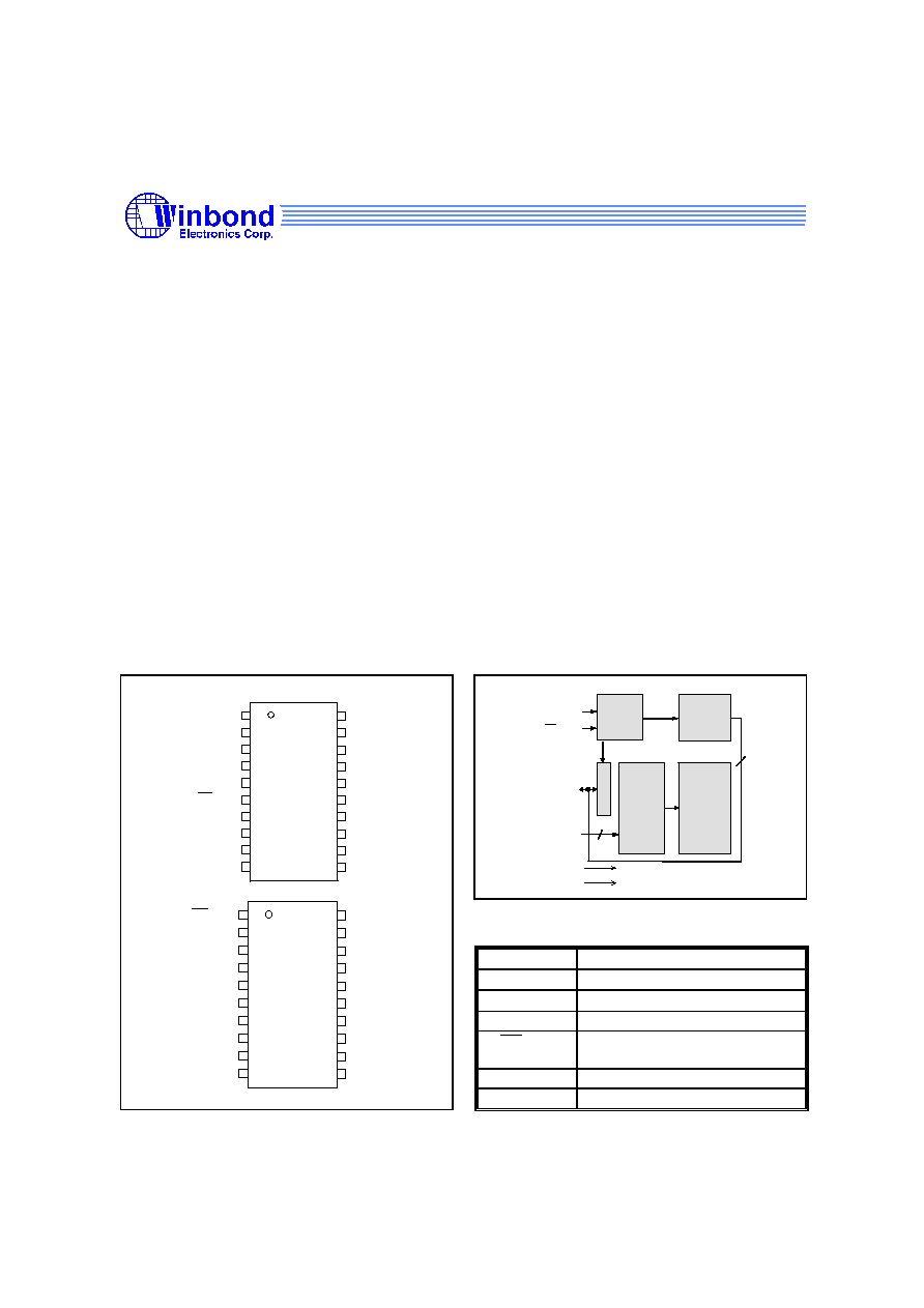
PIN CONFIGURATIONS
1
2
3
4
5
6
7
8
18
19
20
13
14
15
16
17
11
12
9
10
AD2
AD0
AD7
GND
AD6
AD4
AD1
AD3
AD5
A9
A11
A13
A15
OE/VPP
ALE
A14
A12
V
DD
TSSOP
Top View
A10
A8
18
19
20
1
2
3
4
5
6
7
8
13
14
15
17
11
12
9
10
AD5
AD0
A10
A8
AD1
AD3
ALE
A14
A12
GND
AD6
AD4
AD2
A11
A13
A15
SOP
Top View
A9
OE/VPP
VDD
AD7
16
BLOCK DIAGRAM
ALE
OE / V
CONTROL
GND
V
DD
PP
AD7 - AD0
OUTPUT
BUFFER
DECODER
L
A
T
C
H
E
S
A15 - A8
MEMORY
ARRAY
PIN DESCRIPTION
SYMBOL
DESCRIPTION
AD0
-
AD7 Address/Data Inputs/Outputs
A8
-
A15
Address Inputs
ALE
Address Latch Enable
OE /V
PP
Output Enable, Program/Erase
Supply Voltage
V
DD
Power Supply
GND
Ground

W27E520
- 2 -
FUNCTIONAL DESCRIPTION
Read Mode
Unlike conventional UVEPROMs, which has CE and OE two control functions, the W27E520
has one OE /V
PP
and one ALE (address_latch_enable) control functions. The ALE makes lower
address A[7:0] to be latched in the chip when it goes from high to low, so that the same bus can be
used to output data during read mode. i.e. lower address A[7:0] and data bus DQ[7:0] are multiplexed.
OE /V
PP
controls the output buffer to gate data to the output pins. When addresses are stable, the
address access time (T
ACC
) is equal to the delay from ALE to output (T
CE
), and data are available at
the outputs T
OE
after the falling edge of OE /V
PP
, if T
ACC
and T
CE
timings are met.
Erase Mode
The erase operation is the only way to change data from "0" to "1." Unlike conventional UVEPROMs,
which use ultraviolet light to erase the contents of the entire chip (a procedure that requires up to half
an hour), the W27E520 uses electrical erasure. Generally, the chip can be erased within 100 mS by
using an EPROM writer with a special erase algorithm.
There are two ways to enter Erase mode. One is to raise OE /V
PP
to V
PE
(13V), V
DD
= V
DE
(6.5V),
A9 = V
HH
(13V), A10 = high A8&A11 = low, and all other address pins include AD[7:0] keep at fixed
low or high. Pulsing ALE high starts the erase operation. The other way is somewhat like flash, by
programming two consecutive commands into the device and then enter Erase mode. The two
commands are loading Data = AA(hex) to Addr. = 5555(hex) and Data = 10(hex) to Addr. =
2AAA(hex). Be careful to note that the ALE pulse widths of these two commands are different: One is
50uS, while the other is 100mS. Please refer to the Smart Erase Algorithm 1 & 2.
Erase Verify Mode
The device will enter the Erase Verify Mode automatically after Erase Mode. Only power down the
device can force the device enter Normal Read Mode again.
Program Mode
Programming is the only way to change cell data from "1" to "0." The program mode is entered when
OE /V
PP
is raised to V
PP
(13V), V
DD
= V
DP
(6.5V), the address pins equal the desired addresses, and
the input pins equal the desired inputs. Pulsing ALE high starts the programming operation.
Program Verify Mode
The device will enter the Program Verify Mode automatically after Program Mode. Only power down
the device can force the device enter Normal Read Mode again.
Erase/Program Inhibit
Erase or program inhibit mode allows parallel erasing or programming of multiple chips with different
data. When ALE low, erasing or programming of non-target chips is inhibited, so that except for the
ALE and OE /V
PP
pins, the W27E520 may have common inputs.
Standby Mode
The standby mode significantly reduces V
DD
current. This mode is entered when ALE and OE /V
PP
keep high. In standby mode, all outputs are in a high impedance state.

W27E520
Publication Release Date: September 2000
- 3 - Revision A2
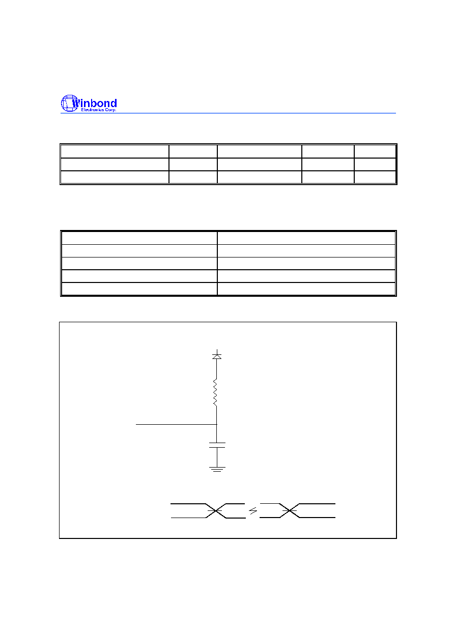
System Considerations
An EPROM's power switching characteristics require careful device decoupling. System designers are
interested in three supply current issues: standby current levels (I
SB
), active current levels (I
DD
), and
transient current peaks produced by the falling and rising edges of ALE Transient current magnitudes
depend on the device output's capacitive and inductive loading. Proper decoupling capacitor selection
will suppress transient voltage peaks. Each device should have a 0.1
µ
F ceramic capacitor connected
between its V
DD
and GND. This high frequency, low inherent-inductance capacitor should be placed
as close as possible to the device. Additionally, for every eight devices, a 4.7
µ
F electrolytic capacitor
should be placed at the array's power supply connection between V
DD
and GND. The bulk capacitor
will overcome voltage slumps caused by PC board trace inductances.
TABLE OF OPERATING MODES
(V
PP
= 13V, V
PE
= 13V, V
HH
= 12V, V
DP
= 6.5V, V
DE
= 6.5V, V
DD
= 5.0V, V
DI
= 5.0V, X = V
IH
or V
IL
)
MODE
PIN
ALE OE/V
PP
OTHER ADDRESS
V
DD
AD[7:0]
Address Latch Enable
V
IH
V
IH
A
IN
V
DD
A[7:0]
Read
V
IL
V
IL
A
IN
V
DD
D
OUT
Output Disable
V
IL
/V
IH
V
IH
X
V
DD
High Z
Standby
V
IH
V
IH
X
V
DD
A[7:0]
Program
V
IH
V
PP
A
IN
V
DP
D
IN
Erase 1
V
IH
V
PE
A8&A11 = V
IL
, A9 = V
PE
,
A10 = V
IH
, Others = X
V
DE
X
Erase 2
V
IH
V
PE
First command:
Addr. = 5555 (hex)
V
DE
AA(hex)
Second command:
Addr. = 2AAA (hex)
V
DE
10(hex)
Product Identifier-
manufacturer
V
IL
V
IL
A8 = V
IL
, A9 = V
HH
, Others = X
V
DI
DA(Hex)
Product Identifier-device V
IL
V
IL
A8 = V
IH
, A9 = V
HH
, Others = X
V
DI
1F(Hex)

W27E520
- 4 -
DC CHARACTERISTICS
Absolute Maximum Ratings
PARAMETER
RATING
UNIT
Ambient Temperature with Power Applied
-55 to +125
∞
C
Storage Temperature
-65 to +150
∞
C
Voltage on all Pins with Respect to Ground Except
OE /V
PP,
A9 and V
DD
Pins
-2.0 to +7.0
V
Voltage on OE /V
PP
Pin with Respect to Ground
-2.0 to +7.0
V
Voltage on A9 Pin with Respect to Ground
-2.0 to +7.0
V
Voltage V
DD
Pin with Respect to Ground
-2.0 to +14.0
V
Notes:
1. Exposure to conditions beyond those listed under Absolute Maximum Ratings may adversely affect the life and reliability
of the device.
2. Minimum voltage is -0.6V DC which may undershoot to -2.0V for pulses of less than 20 nS. Maximum output pin voltage is
V
DD
+0.75V DC which may overshoot to +7.0V for pulses of less than 20 nS.
DC Erase Characteristics
(T
A
= 25
∞
C
±
5
∞
C, V
DD
= 6.5V
±
0.25V)
PARAMETER
SYM.
CONDITIONS
LIMITS
UNIT
MIN. TYP. MAX.
Input Load Current
I
LI
V
IN
= V
IL
or V
IH
-10
-
10
µ
A
V
DD
Erase Current
I
CP
ALE = V
IH,
OE /V
PP
= V
PE
A8 & A11 = V
IL
, A9 = V
PE
,
A10 = V
IH
, Others = X
-
-
30
mA
V
PP
Erase Current
I
PP
ALE = V
IH,
OE /V
PP
= V
PE
A8 & A11 = V
IL
, A9 = V
PE
,
A10 = V
IH
, Others = X
-
-
30
mA
Input Low Voltage
V
IL
-
-0.3
-
0.8
V
Input High Voltage
V
IH
-
2.4
-
V
DD
+0.3
V
Output Low Voltage
(Verify)
V
OL
I
OL
= 2.1 mA
-
-
0.45
V
Output High Voltage
(Verify)
V
OH
I
OH
= -0.4 mA
2.4
-
-
-
A9 SID Voltage
V
HH
V
DD
= 5V
±
10%
11.5
12
12.5
V
A9 Erase Voltage
V
PE
-
12.75 13
13.25
V
V
PP
Erase Voltage
V
PE
-
12.75 13
13.25
V
V
DD
Supply Voltage (Erase
& Erase Verify)
V
DE
-
6.25
6.5
6.75
V
Note: V
DD
must be applied simultaneously or before V
PP
and removed simultaneously or after V
PP
.
W27E520
Publication Release Date: September 2000
- 5 - Revision A2
CAPACITANCE
(V
DD
= 4.5V to 5.5V, T
A
= 25
∞
C, f = 1 MHz)
PARAMETER
SYMBOL
MAX.
UNIT
Input Capacitance
C
IN
V
IN
= 0V
6
pF
Output Capacitance
C
OUT
V
OUT
= 0V
12
pF
AC CHARACTERISTICS
AC Test Conditions
PARAMETER
CONDITIONS
Input Pulse Levels
0V/3V
Input Rise and Fall Times
10 nS
Input and Output Timing Reference Level
1.5V/1.5V
Output Load
C
L
= 100 pF, I
OH
/I
OL
= -0.4 mA/2.1 mA
AC Test Load and Waveforms
+1.3V
3.3K ohm
100 pF (Including Jig and Scope)
D
(IN914)
OUT
3V
0V
1.5V
1.5V
Test Points
Test Points
Input
Output