Document Outline
- Main Menu
- Memory Products
- Search
- Web

Preliminary W27L520
64K
◊
◊
8 ELECTRICALLY ERASABLE EPROM
Publication Release Date: 4/26/2000
- 1 -
Revision A2
GENERAL DESCRIPTION
The W27L520 is a high speed, low power Electrically Erasable and Programmable Read Only
Memory organized as 65,536
◊
8 bits. It includes latches for the lower 8 address lines to multiplex
with the 8 data lines. To cooperate with the MCU, this device could save the external TTL
component, also cost and space. It requires only one supply in the range of 3.0V in normal read
mode. The W27L520 provides an electrical chip erase function. It will be a great convenient when you
need to change/update the contents in the device.
FEATURES
∑
High speed access time: 70/90 nS (max.)
∑
Read operating current: 8 mA (max.)
∑
Erase/Programming operating current
30 mA (max.)
∑
Standby current: 20
µ
A (max.)
∑
Unregulated battery power supply range,
3.0V to 3.6V
∑
+13V erase and programming voltage
∑
High Reliability CMOS Technology
- 2K V ESD Protection
- 200 mA Latchup Immunity
∑
Fully static operation
∑
All inputs and outputs directly LVTTL/CMOS
compatible
∑
Three-state outputs
∑
Available p
ackages: 20-pin TSSOP and 20-pin
SOP
PIN CONFIGURATIONS
1
2
3
4
5
6
7
8
18
19
20
13
14
15
16
17
11
12
9
10
AD2
AD0
AD7
GND
AD6
AD4
AD1
AD3
AD5
A9
A11
A13
A15
OE/VPP
ALE
A14
A12
V
DD
TSSOP
Top View
A10
A8
18
19
20
1
2
3
4
5
6
7
8
13
14
15
17
11
12
9
10
AD5
AD0
A10
A8
AD1
AD3
ALE
A14
A12
GND
AD6
AD4
AD2
A11
A13
A15
SOP
Top View
A9
OE/VPP
VDD
AD7
16
BLOCK DIAGRAM
ALE
OE / V
CONTROL
GND
V
DD
PP
AD7 - AD0
OUTPUT
BUFFER
DECODER
L
A
T
C
H
E
S
A15 - A8
MEMORY
ARRAY
PIN DESCRIPTION
SYMBOL
DESCRIPTION
AD0
-
AD7
Address/Data Inputs/Outputs
A8
-
A15
Address Inputs
ALE
Address Latch Enable
OE /V
PP
Output Enable, Program/Erase
Supply Voltage
V
DD
Power Supply
GND
Ground

Preliminary W27L520
- 2 -
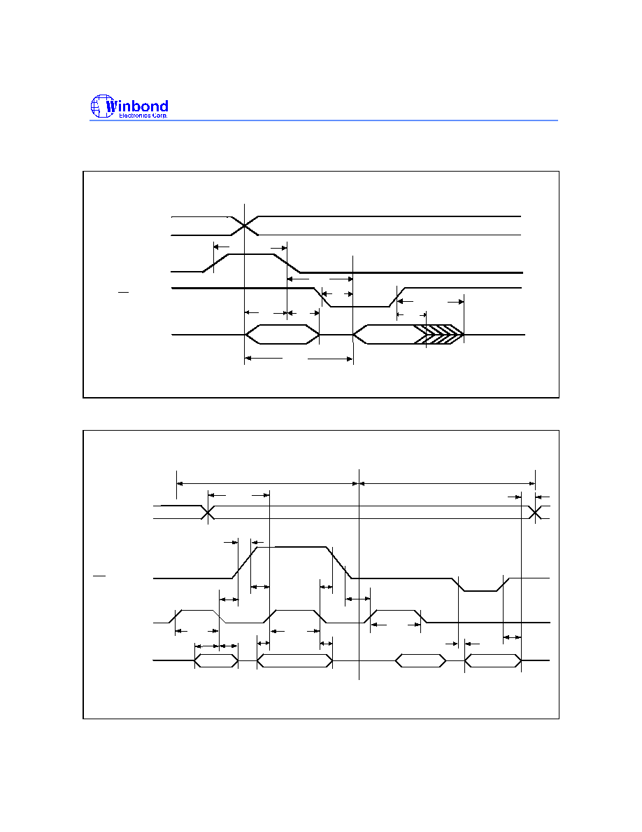
FUNCTIONAL DESCRIPTION
Read Mode
Unlike conventional UVEPROMs, which has CE and OE two control functions, the W27L520 has one
OE /V
PP
and one ALE (address_latch_enable) control functions. The ALE makes lower address A[7:0]
to be latched in the chip when it goes from high to low, so that the same bus can be used to output
data during read mode. i.e. lower address A[7:0] and data bus DQ[7:0] are multiplexed. OE /V
PP
controls the output buffer to gate data to the output pins. When addresses are stable, the address
access time (T
ACC
) is equal to the delay from ALE to output (T
CE
), and data are available at the
outputs T
OE
after the falling edge of OE /V
PP
, if T
ACC
and T
CE
timings are met.
Erase Mode
The erase operation is the only way to change data from "0" to "1." Unlike conventional UVEPROMs,
which use ultraviolet light to erase the contents of the entire chip (a procedure that requires up to half
an hour), the W27L520 uses electrical erasure. Generally, the chip can be erased within 100 mS by
using an EPROM writer with a special erase algorithm.
There are two ways to enter Erase mode. One is to raise OE /V
PP
to V
PE
(13V), V
DD
= V
DE
(6.5V), A9
= V
HH
(13V), A10 = high A8&A11 = low, and all other address pins include AD[7:0] keep at fixed low
or high. Pulsing ALE high starts the erase operation. The other way is somewhat like flash, by
programming two consecutive commands into the device and then enter Erase mode. The two
commands are loading Data = AA(hex) to Addr. = 5555(hex) and Data = 10(hex) to Addr. =
2AAA(hex). Be careful to note that the ALE pulse widths of these two commands are different: One is
50uS, while the other is 100mS. Please refer to the Smart Erase Algorithm 1 & 2.
Erase Verify Mode
The device will enter the Erase Verify Mode automatically after Erase Mode. Only power down the
device can force the device enter Normal Read Mode again.
Program Mode
Programming is the only way to change cell data from "1" to "0." The program mode is entered when
OE /V
PP
is raised to V
PP
(13V), V
DD
= V
DP
(6.5V), the address pins equal the desired addresses, and
the input pins equal the desired inputs. Pulsing ALE high starts the programming operation.
Program Verify Mode
The device will enter the Program Verify Mode automatically after Program Mode. Only power down
the device can force the device enter Normal Read Mode again.
Erase/Program Inhibit
Erase or program inhibit mode allows parallel erasing or programming of multiple chips with different
data. When ALE low, erasing or programming of non-target chips is inhibited, so that except for the
ALE and OE /V
PP
pins, the W27L520 may have common inputs.
Standby Mode
The standby mode significantly reduces V
DD
current. This mode is entered when ALE and OE /V
PP
keep high. In standby mode, all outputs are in a high impedance state.
System Considerations

Preliminary W27L520
Publication Release Date: 4/26/2000
- 3 -
Revision A2
An EPROM's power switching characteristics require careful device decoupling. System designers are
interested in three supply current issues: standby current levels (I
SB
), active current levels (I
DD
), and
transient current peaks produced by the falling and rising edges of ALE Transient current magnitudes
depend on the device output's capacitive and inductive loading. Proper decoupling capacitor selection
will suppress transient voltage peaks. Each device should have a
0.1
µ
F ceramic capacitor connected between its V
DD
and GND. This high frequency, low inherent-
inductance capacitor should be placed as close as possible to the device. Additionally, for every eight
devices, a 4.7
µ
F electrolytic capacitor should be placed at the array's power supply connection
between V
DD
and GND. The bulk capacitor will overcome voltage slumps caused by PC board trace
inductances.
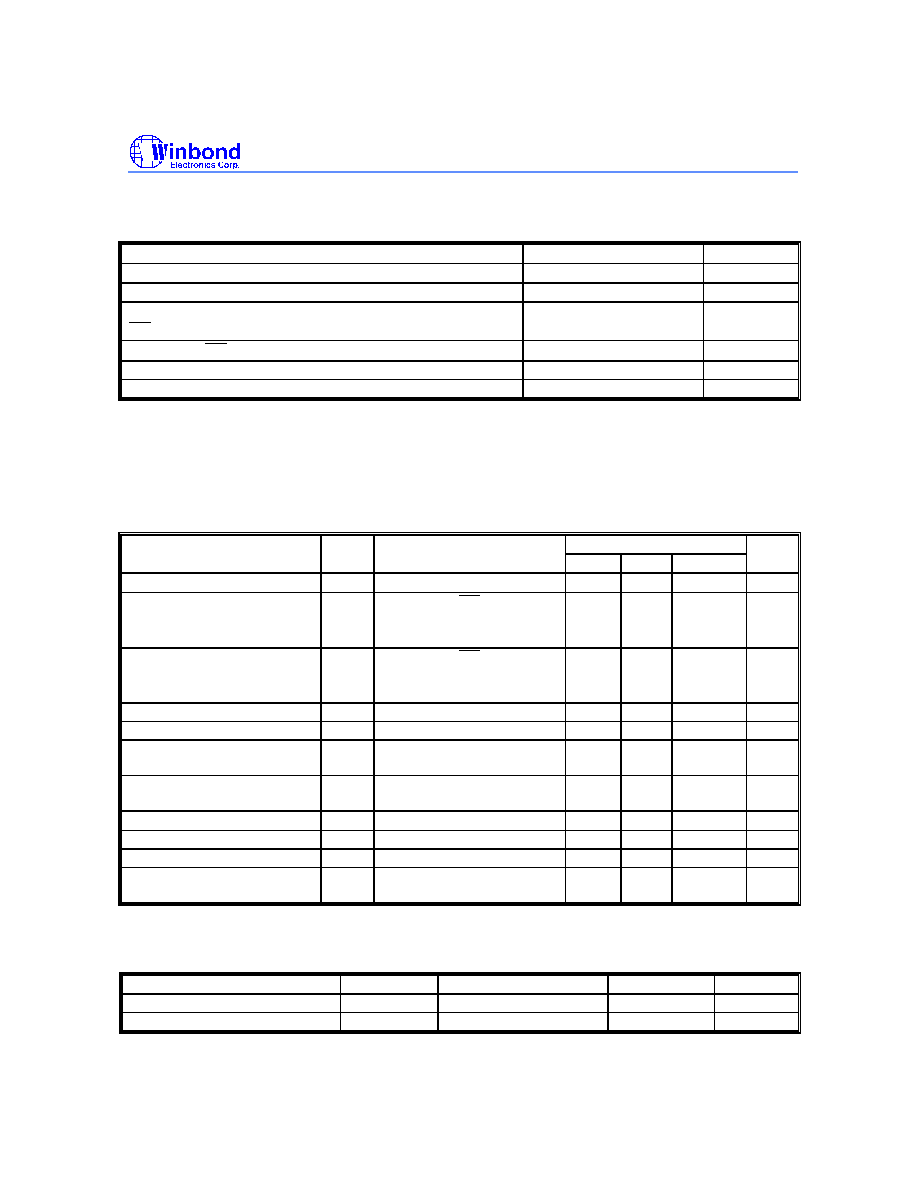
TABLE OF OPERATING MODES
(V
PP
= 13V, V
PE
= 13V, V
HH
= 12V, V
DP
= 6.5V, V
DE
= 6.5V, V
DD
= 3.3V, V
DI
= 5.0V, X = V
IH
or V
IL
)
MODE
PIN
ALE
OE /V
PP
OTHER ADDRESS
V
DD
AD[7:0]
Address Latch Enable
V
IH
V
IH
X
V
DD
A[7:0]
Read
V
IL
V
IL
A
IN
V
DD
D
OUT
Output Disable
V
IL
V
IH
X
V
DD
High Z
Standby
V
IH
V
IH
A
IN
V
DD
A[7:0]
Program
V
IH
V
PP
A
IN
V
DP
D
IN
Erase 1
V
IH
V
PE
A8&A11 = V
IL
, A9 = V
PE
,
A10 = V
IH
, Others = X
V
DE
X
Erase 2
V
IH
V
PE
First command:
Addr. = 5555 (hex)
V
DE
AA(hex)
Secon command:
Addr. = 2AAA (hex)
V
DE
10(hex)
Product Identifier-
manufacturer
V
IL
V
IL
A8 = V
IL
, A9 = V
HH
, Others = X
V
DI
DA(Hex)
Product Identifier-device
V
IL
V
IL
A8 = V
IH
, A9 = V
HH
, Others = X
V
DI
1F(Hex)
Preliminary W27L520
- 4 -
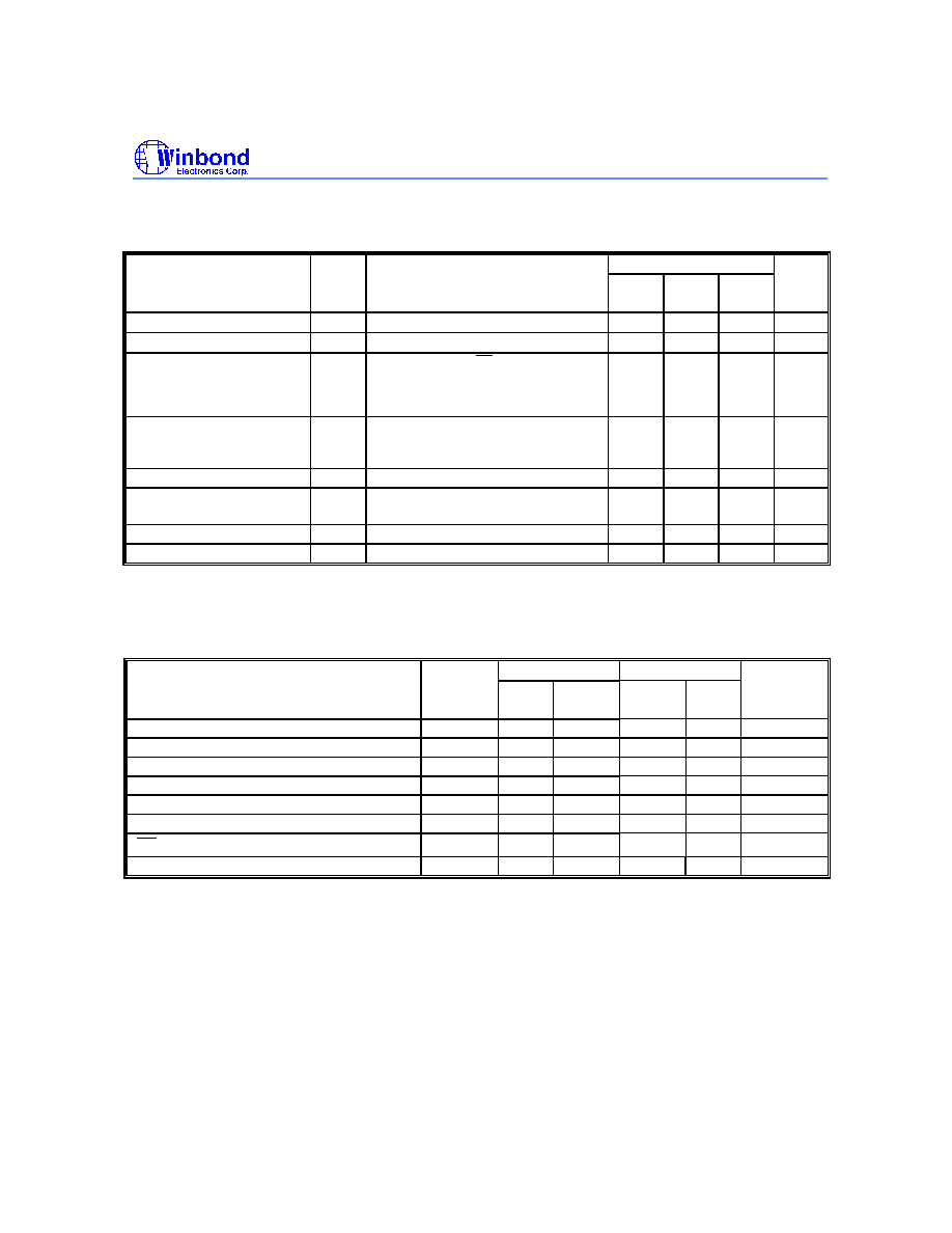
DC CHARACTERISTICS
Absolute Maximum Ratings
PARAMETER
RATING
UNIT
Ambient Temperature with Power Applied
-55 to +125
∞
C
Storage Temperature
-65 to +150
∞
C
Voltage on all Pins with Respect to Ground Except
OE /V
PP,
A9 and V
DD
Pins
-2.0 to +7.0
V
Voltage on OE /V
PP
Pin with Respect to Ground
-2.0 to +7.0
V
Voltage on A9 Pin with Respect to Ground
-2.0 to +7.0
V
Voltage V
DD
Pin with Respect to Ground
-2.0 to +14.0
V
Note: 1. Exposure to conditions beyond those listed under Absolute Maximum Ratings may adversely affect the life and reliability of
the device.
2. Minimum voltage is -0.6V DC which may undershoot to -2.0V for pulses of less than 20ns. Maximum output pin voltage is
V
DD
+0.75V DC which may overshoot to +7.0V for pulses of less than 20ns.
DC Erase Characteristics
(T
A
= 25
∞
C
±
5
∞
C, V
DD
= 6.5V
±
0.25V)
PARAMETER
SYM.
CONDITIONS
LIMITS
UNIT
MIN.
TYP.
MAX.
Input Load Current
I
LI
V
IN
= V
IL
or V
IH
-10
-
10
µ
A
V
DD
Erase Current
I
CP
ALE = V
IH,
OE /V
PP
= V
PE
A8&A11 = V
IL
, A9 = V
PE
,
A10 = V
IH
, Others = X
-
-
30
mA
V
PP
Erase Current
I
PP
ALE = V
IH,
OE /V
PP
= V
PE
A8&A11 = V
IL
, A9 = V
PE
,
A10 = V
IH
, Others = X
-
-
30
mA
Input Low Voltage
V
IL
-
-0.3
-
0.8
V
Input High Voltage
V
IH
-
2.4
-
V
DD
+0.3
V
Output Low Voltage
(Verify)
V
OL
I
OL
= 2.1 mA
-
-
0.45
V
Output High Voltage
(Verify)
V
OH
I
OH
= -0.4 mA
2.4
-
-
-
A9 SID Voltage
V
HH
V
DD
= 5V
±
10%
11.5
12
12.5
V
A9 Erase Voltage
V
PE
-
12.75
13
13.25
V
V
PP
Erase Voltage
V
PE
-
12.75
13
13.25
V
V
DD
Supply Voltage (Erase
& Erase Verify)
V
DE
-
6.25
6.5
6.75
V
Note: V
DD
must be applied simultaneously or before V
PP
and removed simultaneously or after V
PP
.
CAPACITANCE
(V
DD
= 3.0V to 3.6V, T
A
= 25
∞
C, f = 1 MHz)
PARAMETER
SYMBOL
MAX.
UNIT
Input Capacitance
C
IN
V
IN
= 0V
6
pF
Output Capacitance
C
OUT
V
OUT
= 0V
12
pF

Preliminary W27L520
Publication Release Date: 4/26/2000
- 5 -
Revision A2
AC CHARACTERISTICS
AC Test Conditions
PARAMETER
CONDITIONS
Input Pulse Levels
0V/3V
Input Rise and Fall Times
10 nS
Input and Output Timing Reference Level
1.5V/1.5V
Output Load
C
L
= 100 pF, I
OH
/I
OL
= -0.4 mA/2.1 mA
AC Test Load and Waveforms
+1.3V
3.3K ohm
100 pF (Including Jig and Scope)
D
(IN914)
OUT
3V
0V
1.5V
1.5V
Test Points
Test Points
Input
Output
Preliminary W27L520
- 6 -
READ OPERATION DC CHARACTERISTICS
(V
DD
= 3.0V to 3.6V, T
A
= 0 to 70
∞
C)
PARAMETER
SYM.
CONDITIONS
LIMITS
UNIT
MIN.
TYP.
MAX
.
Input Load Current
I
LI
V
IN
= 0V to V
DD
-5
-
5
µ
A
Output Leakage Current
I
LO
V
OUT
= 0V to V
DD
-5
-
5
µ
A
Standby V
DD
Current
(CMOS input)
I
SB
ALE = V
DD
±
0.3V, OE/V
PP
= V
DD
±
0.3V
All others inputs
= GND/ V
DD
±
0.3V
-
-
20
µ
A
V
DD
Operating Current
I
DD
ALE = V
IL
, IOUT = 0 mA
f = 5 MHz
-
-
8
mA
Input Low Voltage
V
IL
-
-0.6
-
0.8
V
Input High Voltage
V
IH
-
2.0
-
V
DD
+0.3
V
Output Low Voltage
V
OL
I
OL
= 2.1 mA
-
-
0.4
V
Output High Voltage
V
OH
I
OH
= -0.4 mA
2.4
-
-
V
READ OPERATION AC CHARACTERISTICS
(V
DD
= 3.0V to 3.6V, T
A
= 0 to 70
∞
C)
PARAMETER
SYM.
W27L520-70
W27L520-90
UNIT
MIN.
MAX.
MIN.
MAX
.
Address Latch Enable Access Time
T
CE
-
70
-
90
nS
Address Latch Enable Width
T
ALE
45
-
45
-
nS
Address Access Time
T
ACC
-
70
-
90
nS
Address Setup Time
T
AS
15
-
15
-
nS
Address Hold Time
T
AH
15
-
15
-
nS
Output Enable Access Time
T
OE
-
35
-
35
nS
OE
/VPP High to High-Z Output
T
DF
-
25
-
25
nS
Output Hold from Address Change
T
OH
0
-
0
-
nS
Note: V
DD
must be applied simultaneously or before V
PP
and removed simultaneously or after V
PP
.

Preliminary W27L520
Publication Release Date: 4/26/2000
- 7 -
Revision A2
DC PROGRAMMING CHARACTERISTICS
(V
DD
= 6.5V
±
0.25V, T
A
= 25
∞
C
±
5
∞
C)
PARAMETER
SYM.
CONDITIONS
LIMITS
UNIT
MIN.
TYP.
MAX.
Input Load Current
I
LI
V
IN
= V
IL
or V
IH
-10
-
10
µ
A
V
DD
Program Current
I
CP
ALE = V
IH
,
OE
/V
PP
= V
PP
-
-
30
mA
V
PP
Program Current
I
PP
ALE = V
IH
,
OE
/V
PP
= V
PP
-
-
30
mA
Input Low Voltage
V
IL
-
-0.3
-
0.8
V
Input High Voltage
V
IH
-
2.4
-
V
DD
+0.5
V
Output Low Voltage (Verify)
V
OL
I
OL
= 2.1 mA
-
-
0.45
V
Output High Voltage (Verify)
V
OH
I
OH
= -0.4 mA
2.4
-
-
V
A9 Silicon I.D. Voltage
V
HH
V
DD
= 5V
±
10%
11.5
12.0
12.5
V
V
PP
Program Voltage
V
PP
-
12.75
13.0
13.25
V
V
DD
Supply Voltage (Program)
V
DP
-
6.25
6.5
6.75
V
AC PROGRAMMING/ERASE CHARACTERISTICS
(V
DD
= 6.5V
±
0.25V, T
A
= 25
∞
C
±
5
∞
C)
PARAMETER
SYM.
LIMITS
UNIT
MIN.
TYP.
MAX.
OE
/V
PP
Pulse Rise Time
T
PRT
50
-
-
nS
Address Latch Enable Width
T
ALE
500
-
-
nS
ALE Program Pulse Width
T
PPW
47.5
50
52.5
µ
S
ALE Erase Pulse Width
T
EPW
95
100
105
mS
ALE Erase Pulse Width 1
T
EPW1
47.5
50
52.5
µ
S
ALE Erase Pulse Width 2
T
EPW2
95
100
105
mS
Latched Address Setup Time
T
LAS
100
-
-
nS
Latched Address Hold Time
T
LAH
100
-
-
nS
Address Setup Time
T
AS
2.0
-
-
µ
S
Address Hold Time
T
AH
0
-
-
µ
S
OE
/V
PP
Setup Time
T
OES
2.0
-
-
µ
S
OE
/V
PP
Hold Time
T
OEH
2.0
-
-
µ
S
Data Setup Time
T
DS
2.0
-
-
µ
S
Data Hold Time
T
DH
2.0
-
-
µ
S
Data Valid from OE /V
PP
Low during Erase Verify
T
EOE
-
-
150
nS
Data Valid from OE /V
PP
Low during Program Verify
T
POE
-
-
150
nS
OE
/V
PP
High to Output High Z
T
DFP
0
-
130
nS
OE
/V
PP
High Voltage Delay After ALE Low
T
VS
2.0
-
-
µ
S
OE
/V
PP
Recovery Time
T
VR
2.0
-
-
µ
S
Note: V
DD
must be applied simultaneously or before V
PP
and removed simultaneously or after V
PP
.
Preliminary W27L520
- 8 -
TIMING WAVEFORMS
AC Read Waveform
OE/Vpp
AD0-AD7
High Z
T
OE
T
OH
T
DF
VIH
VIL
A8-A15
ALE
Address Valid
T
CE
VIL
VIH
VIH
VIL
Address
Data
T
ALE
T
ACC
T
AS
T
AH
High Z
Programming Waveform
ALE
AD[7:0]
PROGRAM
PROGRAM (VERIFY)
VR
POE
DFP
A[15:8]
Address Stable
Add
Data out
T
ALE
T
T
T
13V
V
IH
IL
V
V
IH
IL
V
V
IH
IL
V
V
IH
IL
V
OE/Vpp
T
OES
OEH
VS
ALE
LAS
LAH
DS
PPW
DH
Add
Data in
RPT
T
T
T
T
T
T
T
T
AS
T
T
AH
T

Preliminary W27L520
Publication Release Date: 4/26/2000
- 9 -
Revision A2
Timing Waveforms, continued
Erase Waveform 1
OE/Vpp
13.0V
T
PRT
V
IH
V
IL
ALE
V
IH
V
IL
Address Valid
A[15:8]
V
IH
V
IL
A9 = 12.0V
A9 = 13.0V
Others = V
IL
or V
A8 = V
IL
IH
A8 = V
IH
Others = V
IL
or V
A8, A11 = V
IL
IH
A10 = V
IH
AD[7:0]
DA
1F
D
OUT
V
IH
V
IL
Add
T
EPW
T
VR
T
OES
T
OEH
T
EOE
Read
Company
SID
Chip Erase
Erase (Verify)
Read
Device
SID
V = 6.5V
DD
V =3.3V
DD
V = 6.5V
DD
Erase Waveform 2
OE/Vpp
13.0V
T
PRT
V
IH
V
IL
ALE
V
IH
V
IL
A[15:8]
V
IH
V
IL
A9=12.0
V
Others=V
IL
or V
A8=V
IL
IH
A8=V
IH
AD[7:0]
DA
1F
V
IH
V
IL
Address Valid
D
OUT
Add
T
EOE
Read
Company
SID
Command 1
Command 2
Read
Device
SID
OES
OEH
VS
T
RPT
T
T
T
T
OES
ALE
LAS
LAH
DS
EPW1
DH
55
AA
T
T
T
T
T
AS
T
T
AA
10
Erase Verify
Chip Erase
EPW2
T
A[15:8] = 55
A[15:8] = 2A
V =3.3V
DD
V =6.5V
DD
V =6.5V
DD
V =6.5V
DD
Note: First command Address = 5555(hex) with Data = AA(hex)
Second command Address = 2AAA(hex) with Data = 10(hex)
Preliminary W27L520
- 10 -
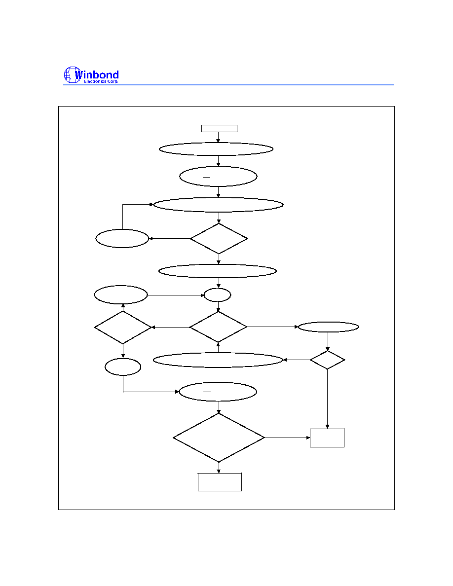
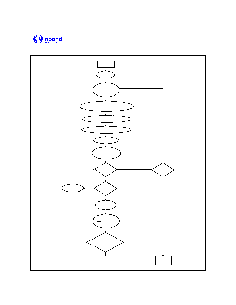
SMART PROGRAMMING ALGORITHM 1
Start
Address = First Location
OE/Vpp = 13V
Program One 50 S Pulse
Last
Address ?
Address = First Location
X = 0
Verify
Byte
Program One 50 S Pulse
OE/Vpp = V
IL
Compare
All Bytes to
Data
Original
Device
Passed
Pass
Yes
Increment
Address
No
Increment
Address
Last
Address ?
No
Pass
Yes
Increment X
Fail
X = 25 ?
No
Device
Yes
Fail
Failed
µ
µ
Power
Down
V = 6.5V
DD
V = 3.3V
DD

Preliminary W27L520
Publication Release Date: 4/26/2000
- 11 -
Revision A2
SMART PROGRAMMING ALGORITHM 2
Start
Address = First Location
Program One 50 S Pulse
Compare
All Bytes to
Data
Original
Device
Passed
Pass
Increment
Address
No
Increment X
Fail
Device
Failed
µ
X = 0
X = 25?
Yes
Last Address
?
Yes
No
Pass
Fail
Fail
Pass
OE/Vpp = 13V
OE/Vpp = V
IL
Verify One Byte
OE/Vpp = V
IL
Verify One Byte
Power
Down
V =3.3V
DD
V = 6.5V
DD
Preliminary W27L520
- 12 -
SMART ERASE ALGORITHM 1
Start
OE/Vpp = 13V
Last
Address?
OE/Vpp = V
Compare
All Bytes to
FFs (HEX)
Pass
Device
Increment
Address
No
Fail
Fail
Fail
Device
X = 0
A9 = 13V; A8&A11 = V
A10 = V
Chip Erase 100 mS Pulse
Address = First Location
Erase
Verify
X = 20?
No
Yes
Pass
Pass
Yes
OE/Vpp = V
IL
IL
Increment X
IL
IH
Power
Down
DD
V = 6.5V
V = 6.5V
DD
V = 3.3V
DD

Preliminary W27L520
Publication Release Date: 4/26/2000
- 13 -
Revision A2
SMART ERASE ALGORITHM 2
Start
OE/Vpp = 13V
Last
Address?
OE/Vpp = V
Compare
All Bytes to
FFs (HEX)
Pass
Device
Increment
Address
No
Fail
Fail
Fail
Device
X = 0
Program One 50 S Pulse
with Address = 5555(Hex) Data = AA(Hex)
Erase
Verify
X = 20?
No
Yes
Pass
Pass
Yes
OE/Vpp = V
IL
IL
Increment X
Power
Down
Program One 100 mS Pulse
with Address = 2AAA(Hex) Data = 10(Hex)
µ
V = 6.5V
DD
V = 6.5V
DD
V = 3.3V
DD
Preliminary W27L520
- 14 -
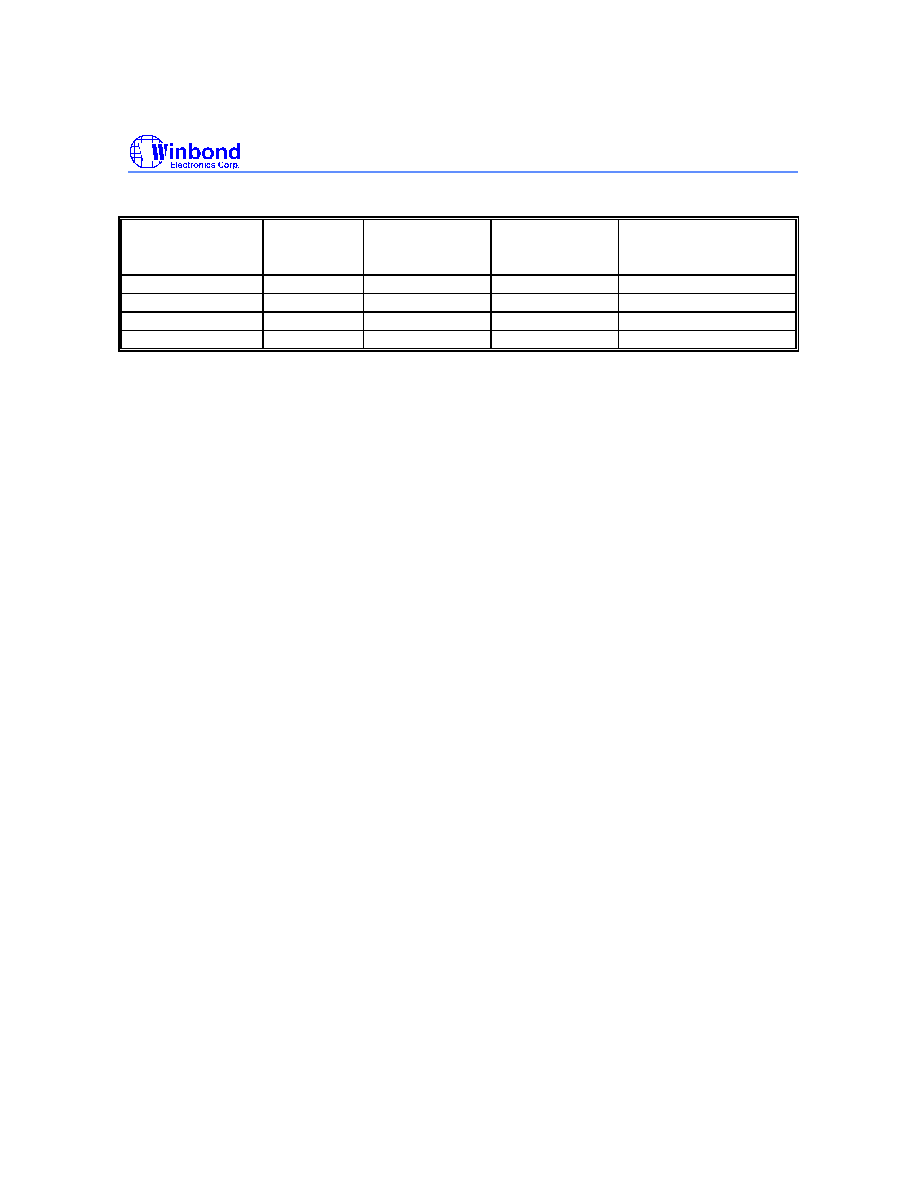
ORDERING INFORMATION
PART NO.
ACCESS
TIME
(nS)
OPERATING
CURRENT
MAX. (mA)
STANDBY
CURRENT
MAX. (
µ
µ
A)
PACKAGE
W27L520W-70*
70
8
20
173mil TSSOP
W27L520W-90*
90
8
20
173mil TSSOP
W27L520S-70*
70
8
20
300mil SOP
W27L520S-90*
90
8
20
300mil SOP
Notes:
1. The Part No is preliminary and might be changed after project is consoled.
2. Winbond reserves the right to make changes to its products without prior notice.
3. Purchasers are responsible for performing appropriate quality assurance testing on products intended for use in applications
where personal injury might occur as a consequence of product failure.

Preliminary W27L520
Publication Release Date: 4/26/2000
- 15 -
Revision A2
PACKAGE DIMENSIONS
20-pin TSSOP
Dimension in mm
Dimension in Inches
Min.
Nom. Max.
Symbol
A
b
c
A
e
0.002
0.09
0.043
0.006
0.18
0.256 BSC
1.10
0.15
L
0.50
0.70
0.028
0.020
E
E
4.30
4.48
0.169
0.176
0.003
0.007
0.65 BSC
0.05
Min.
Nom. Max.
E
E
b
e
D
A
A
c
L
1
1
1
1
D
6.40
6.60
0.260
0.252
6.25
6.50
0.256
0.246
0.18
0.30
0.012
0.007
0
8
0
8
20-pin SOP
Dimension in mm
Dimension in Inches
Min.
Nom. Max.
Symbol
A
b
c
A
e
0.003
0.229
0.105
0.012
0.330
1.27 BSC
2.67
0.305
L
0.381
0.889
0.035
0.015
E
E
7.39
7.60
0.291
0.299
0.009
0.013
0.50 BSC
0.076
Min.
Nom. Max.
E
E
b
e
D
A
A
c
L
1
1
1
1
D
12.6
13.0
0.513
0.497
9.98
10.7
0.420
0.393
0.330
0.508
0.020
0.013
0
8
0
8
0.092
2.34

Preliminary W27L520
- 16 -
VERSION HISTORY
VERSION
DATE
PAGE
DESCRIPTION
A1
Sep. 1999
-
Initial Issued
A2
Feb. 2000
3, 4, 9, 11
Specify V
DD
, V
ID
, V
CE,
and V
HH
description
1
Change V
CC
as V
DD
4
Change V
CE
as V
DE
6, 7, 8, 9, 10 Change V
CE
as V
DE,
V
CP
as V
DP,
V
ID
as V
HH,
I
CC
as I
DD
1,6,14
Add 90nS bin
1,3,6
Add in power supply range: 4.5V to 5.5V
5
AC Test Condition: Change Input pulse level to 0V/3V;
Input and Output Timing Reference Level to 1.5V/1.5V
3/14/2000
3
Delete Two-line Output Control section
4
Modify Storage Temperature Rating from -65 to
+125
∞
C to -65 to +150
∞
C
6
Modify Output Leakage Current from
±
10
µ
A to
±
5
µ
A
4/26/2000
1,3,6
Delete power supply range: 4.5V to 5.5V
1
Add in ESD/Latchup information
4
Modify DC Characteristics
Headquarters
No. 4, Creation Rd. III,
Science-Based Industrial Park,
Hsinchu, Taiwan
TEL: 886-3-5770066
FAX: 886-3-5796096
http://www.winbond.com.tw/
Voice & Fax-on-demand: 886-2-7197006
Taipei Office
11F, No. 115, Sec. 3, Min-Sheng East Rd.,
Taipei, Taiwan
TEL: 886-2-7190505
FAX: 886-2-7197502
Winbond Electronics (H.K.) Ltd.
Rm. 803, World Trade Square, Tower II,
123 Hoi Bun Rd., Kwun Tong,
Kowloon, Hong Kong
TEL: 852-27513100
FAX: 852-27552064
Winbond Electronics North America Corp.
Winbond Memory Lab.
Winbond Microelectronics Corp.
Winbond Systems Lab.
2727 N. First Street, San Jose,
CA 95134, U.S.A.
TEL: 408-9436666
FAX: 408-5441798
Note: All data and specifications are subject to change without notice.