
W28J321B/T
32M(2M
� 16)
BOOT BLOCK FLASH MEMORY
Publication Release Date: April 11, 2003
- 1 -
Revision A4
Table of Contents-
1. GENERAL DESCRIPTION.................................................................................................................. 3
2. FEATURES ......................................................................................................................................... 3
3. PRODUCT OVERVIEW ...................................................................................................................... 4
4. BLOCK DIAGRAM .............................................................................................................................. 5
Block Organization ........................................................................................................................... 6
5. PIN CONFIGURATION ....................................................................................................................... 6
6. PIN DESCRIPTION............................................................................................................................. 7
7. PRINCIPLES OF OPERATION........................................................................................................... 8
Data Protection ................................................................................................................................ 8
8. BUS OPERATION............................................................................................................................. 11
Read............................................................................................................................................... 11
Output Disable ............................................................................................................................... 11
Standby .......................................................................................................................................... 11
Reset .............................................................................................................................................. 11
Read Identifier Codes .................................................................................................................... 12
OTP(One Time Program) Block..................................................................................................... 13
Write ............................................................................................................................................... 14
9. COMMAND DEFINITIONS................................................................................................................ 14
Read Array Command ................................................................................................................... 16
Read Identifier Codes Command................................................................................................... 16
Read Status Register Command ................................................................................................... 16
Clear Status Register Command ................................................................................................... 17
Block Erase Command .................................................................................................................. 17
Full Chip Erase Command ............................................................................................................. 17
Word Write Command.................................................................................................................... 18
Block Erase Suspend Command ................................................................................................... 18
Word Write Suspend Command .................................................................................................... 19
Set Block and Permanent Lock-Bit Commands............................................................................. 19
Clear Block Lock-Bits Command ................................................................................................... 20
OTP Program Command ............................................................................................................... 20
Block Locking by the #WP ............................................................................................................. 21

W28J321B/T
- 2 -
10. DESIGN CONSIDERATIONS ......................................................................................................... 31
Three-Line Output Control ............................................................................................................. 31
Power Supply Decoupling .............................................................................................................. 31
V
PP
Trace on Printed Circuit Boards .............................................................................................. 31
V
DD
, V
PP
, #RESET Transitions ....................................................................................................... 31
Power-up/Down Protection ............................................................................................................ 32
Power Dissipation .......................................................................................................................... 32
Data Protection Method ................................................................................................................. 32
11. ELECTRICAL SPECIFICATIONS ................................................................................................... 33
Absolute Maximum Ratings* .......................................................................................................... 33
Operating Conditions ..................................................................................................................... 33
Capacitance(1)............................................................................................................................... 33
AC Input/Output Test Conditions ................................................................................................... 34
DC Characteristics ......................................................................................................................... 35
AC Characteristics - Read-only Operations(1) .............................................................................. 37
AC Characteristics - Write Operations(1) ...................................................................................... 38
Alternative #CE - Controlled Writes(1)........................................................................................... 40
Reset Operations ........................................................................................................................... 42
Block Erase, Full Chip Erase, Word Write And Lock-Bit Configuration Performance(3)............... 43
12. ADDITIONAL INFORMATION......................................................................................................... 44
Recommended Operating Conditions............................................................................................ 44
13. ORDERING INFORMATION........................................................................................................... 46
14. PACKAGE DIMENSION.................................................................................................................. 46
15. VERSION HISTORY ....................................................................................................................... 47

W28J321B/T
1. GENERAL DESCRIPTION
The W28J321B/T Flash memory chip is a high-density, cost-effective, nonvolatile, read/write storage
device suited for a wide range of applications. It operates off of V
DD
= 2.7V to 3.6V, with V
PP
of 2.7V to
3.6V or 11.7V to 12.3V. This low voltage operation capability enbales use in low power applications.
The IC features a boot, parameter and main-blocked architecture, as well as low voltage and
extended cycling. These features provide a highly flexible device suitable for portable terminals and
personal computers. Additionally, the enhanced suspend capabilities provide an ideal solution for both
code and data storage applications. For secure code storage applications, such as networking where
code is either directly executed out of flash or downloaded to DRAM, the device offers four levels of
protection. These are: absolute protection, enabled when V
PP
V
PPLK
; selective hardware block
locking; flexible software block locking; or write protection. These alternatives give designers
comprehensive control over their code security needs. The device is manufactured using 0.25
�m
process technology. It comes in chip-size package: the 0.75 mm pitch 48-ball TFBGA, which makes it
ideal for small real estate applications.
2. FEATURES
�
Low Voltage Operation
- V
DD
= V
PP
= 2.7V to 3.6V Single Voltage
�
OTP (One Time Program) Block
- 3963 word + 4 word Program only array
�
16bit I/O Interface
�
High-Performance Read Access Time
- 90 nS (V
DD
= 2.7V to 3.6V)
�
Operating Temperature
- -40� C to +85� C
�
Low Power Management
- 4 �A (V
DD
= 3.0V) Typical Standby Current
- Automatic Power Savings Mode Decreases
I
CCR
in Static Mode
- 120 �A (V
DD
= 3.0V, T
A
= +25
� C, f = 32 KHz)
Typical Read Current
�
Optimized Array Blocking Architecture
- Two 4k-word Boot Blocks
- Six 4k-word Parameter Blocks
- Sixty-three 32k-word Main Blocks
- Top or Bottom Boot Location
�
Extended Cycling Capability
- Minimum 100,000 Block Erase Cycles
�
Enhanced Automated Suspend Options
- Word Write Suspend to Read
- Block Erase Suspend to Word Write
- Block Erase Suspend to Read
�
Enhanced Data Protection Features
- Absolute Protection with V
PP
V
PPLK
- Block Erase, Full Chip Erase, Word Write
and Lock-Bit Configuration Lockout during
Power Transitions
- Block Locking with Command and #WP
- Permanent Locking
�
Automated Block Erase, Full Chip Erase, Low
Power Management Word Write and Lock-Bit
Configuration
- Command User Interface (CUI)
- Status Register (SR)
�
SRAM-Compatible Write Interface
�
Chip-Size Packaging
- 0.75 mm pitch 48-Ball TFBGA
� Nonvolatile Flash Technology
� CMOS Process (P-type silicon substrate)
� Not designed or rated as radiation hardened
Publication Release Date: April 11, 2003
- 3 -
Revision A4

W28J321B/T
- 4 -
3. PRODUCT OVERVIEW
The W28J321B/T is a high-performance 32M-bit Boot Block Flash memory organized as 2M-word of
16 bits. The 2M-word of data is arranged in two 4k-word boot blocks, six 4k-word parameter blocks
and sixty-three 32k-word main blocks which are individually erasable, lockable and unlockable in-
system. The memory map is shown in Figure 3.
The dedicated V
PP
pin gives complete data protection when V
PP
V
PPLK
.
A Command User Interface (CUI) serves as the interface between the system processor and internal
operation of the device. A valid command sequence written to the CUI initiates device automation. An
internal Write State Machine (WSM) automatically executes the algorithms and timings necessary for
block erase, full chip erase, word write and lock-bit configuration operations.
A block erase operation erases one of the device's 32Kword blocks typically within 1.2s (3V V
DD
, 3V
V
PP
), 4k-word blocks typically within 0.6s (3V V
DD
, 3V V
PP
) independent of other blocks. Each block
can be independently erased minimum 100,000 times. Block erase suspend mode allows system
software to suspend block erase to read or write data from any other block.
Writing memory data is performed in word increments of the device's 32k-word blocks typically within
33�s (3V V
DD
, 3V V
PP
), 4k-word blocks typically within 36
�S (3V V
DD
, 3V V
PP
). Word write suspend
mode enables the system to read data or execute code from any other flash memory array location.
Individual block locking uses a combination of bits, seventy-one block lock-bits, a permanent lock-bit
and #WP pin, to lock and unlock blocks. Block lock-bits gate block erase, full chip erase and word
write operations, while the permanent lock-bit gates block lock-bit modification and locked block
alternation. Lock-bit configuration operations (Set Block Lock-Bit, Set Permanent Lock-Bit and Clear
Block Lock-Bits commands) set and cleared lock-bits.
The status register indicates when the WSM's block erase, full chip erase, word write or lock-bit
configuration operation is finished.
The access time is 90 nS (t
AVQV
) over the operating temperature range (-40
� C to +85� C) and V
DD
supply voltage range of 2.7V to 3.6V.
The Automatic Power Savings (APS) feature substantially reduces active current when the device is in
static mode (addresses not switching). In APS mode, the typical I
CCR
current is 4
�A (CMOS) at 3.0V
V
DD
.
When #CE and #RESET pins are at V
DD
, the I
CC
CMOS standby mode is enabled. When the #RESET
pin is at Vss, reset mode is enabled which minimizes power consumption and provides write
protection. A reset time (t
PHQV
) is required from #RESET switching high until outputs are valid.
Likewise, the device has a wake time (t
PHEL
) from #RESET-high until writes to the CUI are recognized.
With #RESET at V
SS
, the WSM is reset and the status register is cleared.
Overwriting a "0" to a bit already holding a data "0" may render this bit un-erasable. In order to avoid
this potential "stuck bit" failure, when re-programming (changing data from "1" to "0") the following
should be followed:
� Program "0" for the bit in which you want to change data from "1" to "0".
� Program "1" for the bit which is already holding a data "0". (Note: Since only an erase process
can change the data from "0" to "1", programming "1" to a bit holding a data "0" will not
change the data).
For example, changing data from "10111101" to "10111100" requires "11111110" programming.

W28J321B/T
Publication Release Date: April 11, 2003
- 5 -
Revision A4
4. BLOCK DIAGRAM
g
32K-Word
(64K-Byte)
Main Blocks
x 63
Output Buffer
DQ0 -DQ15
Input Buffer
Identifier
Register
Output
Multiplexer
Status
Register
Data
Register
Command
User
Interface
I/O Logic
Data
Comparator
Y-Gatin
M
a
i
n
B
l
o
ck 0
M
a
i
n
B
l
o
ck 1
Input
Buffer
Address
Latch
Address
Counter
Y
Decoder
X
Decoder
Write
State
Machine
Program/Erase
Voltage Switch
VDD
#CE
#WE
#OE
#RESET
#WP
RY/#BY
VPP
VDD
VSS
A0-A20
P
a
ra
m
e
te
r B
l
o
ck 0
P
a
ra
m
e
te
r B
l
o
ck 1
P
a
ra
m
e
te
r B
l
o
ck 2
P
a
ra
m
e
te
r B
l
o
ck 3
P
a
ra
m
e
te
r B
l
o
ck 4
P
a
ra
m
e
te
r B
l
o
ck 5
Boot Bloc
k
0
Boot Bloc
k
1
Main Bloc
k
61
Main Bloc
k
62
O
T
P Bloc
k
Figure 1. Block Diagram

W28J321B/T
- 6 -
Block Organization
This product features an asymmetrically-blocked architecture providing system memory integration.
Each erase block can be erased independently of the others up to 100,000 times. For the address
locations of the blocks, see the memory map in Figure 3.
Boot Blocks: The boot block is intended to replace a dedicated boot PROM in a microprocessor or
microcontroller-based system. This boot block 4k words (4,096 words) features hardware controllable
write protection to protect the crucial microprocessor boot code from accidental modification. The
protection of the boot block is controlled using a combination of the V
PP
, #RESET, #WP pins and block
lock-bit.
Parameter Blocks: The boot block architecture includes parameter blocks to facilitate storage of
frequently update small parameters that would normally require an EEPROM. By using software
techniques, the word-rewrite functionality of EEPROMs can be emulated. Each boot block component
contains six parameter blocks of 4k words (4,096 words) each. The protection of the parameter block
is controlled using a combination of the V
PP
, #RESET and block lock-bit.
Main Blocks: The reminder is divided into main blocks for data or code storage. Each 32M-bit device
contains sixty-three 32k words (32,768 words) blocks. The protection of the main block is controlled
using a combination of the V
PP
, #RESET and block lock-bit.
5. PIN CONFIGURATION
A
#CE
A3
B
C
D
E
F
G
H
A4
A2
A1
A0
#OE
A7
A17
A6
A5
DQ0
DQ8
DQ9
DQ1
A18
A20
DQ2
DQ10
DQ11
DQ3
#WP
#WE
#RESET
NC
A19
DQ5
DQ12
V
DD
DQ4
A9
A8
A10
A11
DQ7
DQ14
DQ13
DQ6
A13
A12
A14
A15
A16
DQ15
Vss
Vss
V
DD
V
PP
1
2
3
4
5
6
0. 75mm pitch
48-Ball TFBGA
Pinout
8 x 11 mm
TOP VIEW
Figure 2. 0.75 mm pitch TFBGA 48-Ball Pinout
W28J321B/T
Publication Release Date: April 11, 2003
- 7 -
Revision A4
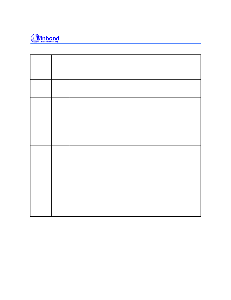
6. PIN DESCRIPTION
SYMBOL
TYPE
NAME AND FUNCTION
A0
- A20
INPUT
ADDRESS INPUTS: Inputs for addresses during read and write operations.
Addresses are internally latched during a write cycle.
A15
- A20: Main Block Address.
A12
- A20: Boot and Parameter Block Address.
DQ0
- DQ15
INPUT/
OUTPUT
DATA INPUT/OUTPUTS: Inputs data and commands during CUI write cycles;
outputs data during memory array, status register and identifier code read cycles.
Data pins float to high impedance when the chip is deselected or outputs are
disabled. Data is internally latched during write cycle.
#CE INPUT
CHIP ENABLE: Activates the device's control logic, input buffers, decoders and
sense amplifiers.
#CE-high deselects the device and reduces power consumption to standby levels.
#RESET INPUT
RESET: Resets the device internal automation. #RESET-high enables normal
operation. When driven low, #RESET inhibits write operations which provides data
protection during power transitions. Exit from reset mode sets the device to read array
mode. #RESET must be V
IL
during power-up.
#OE INPUT
OUTPUT ENABLE: Gates the device's outputs during a read cycle.
#WE INPUT
WRITE ENABLE: Controls writes to the CUI and array blocks. Addresses and data
are latched on the rising edge of the #WE pulse.
#WP INPUT
WRITE PROTECT: When #WP is V
IL
, boot blocks cannot be written or erased. When
#WP is V
IH
, locked boot blocks can not be written or erased. #WP is not affected
parameter and blocks.
V
PP
SUPPLY
BLOCK ERASE, FULL CHIP ERASE, WORD WRITE OR LOCK-BIT
CONFIGURATION POWER SUPPLY: For erasing array blocks, writing words or
configuring lock-bits. With V
PP
V
PPLK
, memory contents cannot be altered. Block
erase, full chip erase, word write and lock-bit configuration with an invalid V
PP
(see
DC Characteristics) produce spurious results and should not be attempted. Applying
12V
�0.3V to V
PP
during erase/write can only be done for a maximum of 1000 cycles
on each block. V
PP
may be connected to 12V
�0.3V for a total of 80 hours maximum.
V
DD
SUPPLY
DEVICE POWER SUPPLY: Do not float any power pins. With V
DD
V
LKO
, all write
attempts to the flash memory are inhibited. Device operations at invalid V
DD
voltage
(see DC Characteristics) produce spurious results and should not be attempted.
V
SS
SUPPLY
GROUND: Do not float any ground pins.
NC
NO CONNECT: Lead is not internal connected; it may be driven or floated.
Table 1.

W28J321B/T
- 8 -
7. PRINCIPLES OF OPERATION
The W28J321B/T flash memory includes an on-chip WSM to manage block erase, full chip erase,
word write and lock-bit configuration functions. It allows for: fixed power supplies during block erase,
full chip erase, word write and lock-bit configuration, and minimal processor overhead with RAM-like
interface timings.
After initial device power-up or return from reset mode (see Bus Operations section), the device
defaults to read array mode. Manipulation of external memory control pins allow array read, standby
and output disable operations.
Status register and identifier codes can be accessed through the CUI independent of the V
PP
voltage.
High voltage on V
PP
enables successful block erase, full chip erase, word write and lock-bit
configurations. All functions associated with altering memory contents (block erase, full chip erase,
word write, lock-bit configuration, status and identifier codes) are accessed via the CUI and verified
through the status register.
Commands are written using standard microprocessor write timings. The CUI contents serve as input
to the WSM, which controls the block erase, full chip erase, word write and lock-bit configuration. The
internal algorithms are regulated by the WSM, including pulse repetition, internal verification and
margining of data. Addresses and data are internally latched during write cycles. Writing the
appropriate command outputs array data, accesses the identifier codes or outputs status register
data.
Interface software that initiates and polls progress of block erase, full chip erase, word write and lock-
bit configuration can be stored in any block. This code is copied to and executed from system RAM
during flash memory updates. After successful completion, reads are again possible via the Read
Array command. Block erase suspend allows system software to suspend a block erase to read/write
data from/to blocks other than that which is suspend. Word write suspend allows system software to
suspend a word write to read data from any other flash memory array location.
Data Protection
When V
PP
V
PPLK
, memory contents cannot be altered. The CUI, with two-step block erase, full chip
erase, word write or lock-bit configuration command sequences, provides protection from unwanted
operations even when high voltage is applied to V
PP
. All write functions are disabled when V
DD
is
below the write lockout voltage V
LKO
or when #RESET is at V
IL
. The device's block locking capability
provides additional protection from inadvertent code or data alteration by gating block erase, full chip
erase and word write operations. Refer to Table 5 for write protection alternatives.
W28J321B/T
Publication Release Date: April 11, 2003
- 9 -
Revision A4
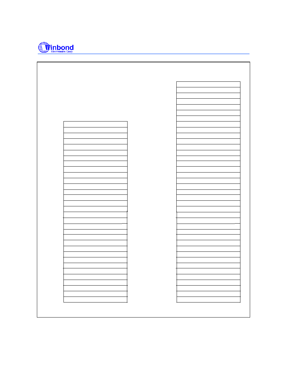
[A20-A0]
32KW/64KB Main Block 32
32KW/64KB Main Block 33
32KW/64KB Main Block 34
32KW/64KB Main Block 35
32KW/64KB Main Block 36
32KW/64KB Main Block 37
32KW/64KB Main Block 38
32KW/64KB Main Block 39
32KW/64KB Main Block 40
32KW/64KB Main Block 41
32KW/64KB Main Block 42
32KW/64KB Main Block 43
32KW/64KB Main Block 44
32KW/64KB Main Block 45
32KW/64KB Main Block 46
0A8000
090000
088000
080000
078000
068000
060000
058000
050000
070000
0B7FFF
0B0000
0AFFFF
0A7FFF
0A0000
09FFFF
098000
097FFF
08FFFF
087FFF
07FFFF
077FFF
06FFFF
067FFF
05FFFF
057FFF
04FFFF
048000
047FFF
040000
03FFFF
038000
037FFF
030000
02FFFF
028000
027FFF
020000
01FFFF
018000
017FFF
010000
00FFFF
008000
007FFF
000000
32KW/64KB Main Block 47
32KW/64KB Main Block 48
32KW/64KB Main Block 49
32KW/64KB Main Block 50
32KW/64KB Main Block 51
32KW/64KB Main Block 52
32KW/64KB Main Block 53
32KW/64KB Main Block 54
32KW/64KB Main Block 55
32KW/64KB Main Block 56
32KW/64KB Main Block 57
32KW/64KB Main Block 58
32KW/64KB Main Block 59
32KW/64KB Main Block 60
32KW/64KB Main Block 61
32KW/64KB Main Block 62
0C0000
0B8000
0C8000
0E7FFF
0D8000
0DFFFF
0D7FFF
0FFFFF
0F7FFF
0EFFFF
0F8000
0F0000
0E8000
0E0000
0D0000
0CFFFF
0C7FFF
0BFFFF
Top Boot
[A20-A0]
4KW/8KB Boot Block 0
4KW/8KB Boot Block 1
4KW/8KB Parameter Block 0
4KW/8KB Parameter Block 1
4KW/8KB Parameter Block 2
4KW/8KB Parameter Block 3
4KW/8KB Parameter Block 4
4KW/8KB Parameter Block 5
32KW/64KB Main Block 0
32KW/64KB Main Block 1
32KW/64KB Main Block 2
32KW/64KB Main Block 3
32KW/64KB Main Block 4
32KW/64KB Main Block 5
32KW/64KB Main Block 6
32KW/64KB Main Block 7
32KW/64KB Main Block 8
32KW/64KB Main Block 9
32KW/64KB Main Block 10
32KW/64KB Main Block 11
32KW/64KB Main Block 12
32KW/64KB Main Block 13
32KW/64KB Main Block 14
1A8000
190000
188000
180000
178000
168000
160000
158000
150000
170000
1B7FFF
1B0000
1AFFFF
1A7FFF
1A0000
19FFFF
198000
197FFF
18FFFF
187FFF
17FFFF
177FFF
16FFFF
167FFF
15FFFF
157FFF
14FFFF
148000
147FFF
140000
13FFFF
138000
137FFF
130000
12FFFF
128000
127FFF
120000
11FFFF
118000
117FFF
110000
10FFFF
108000
107FFF
100000
32KW/64KB Main Block 15
32KW/64KB Main Block 16
32KW/64KB Main Block 17
32KW/64KB Main Block 18
32KW/64KB Main Block 19
32KW/64KB Main Block 20
32KW/64KB Main Block 21
32KW/64KB Main Block 22
32KW/64KB Main Block 23
32KW/64KB Main Block 24
32KW/64KB Main Block 25
32KW/64KB Main Block 26
32KW/64KB Main Block 27
32KW/64KB Main Block 28
32KW/64KB Main Block 29
32KW/64KB Main Block 30
1C0000
1B8000
1C8000
1E7FFF
1D8000
1DFFFF
1D7FFF
1F9FFF
1F8FFF
1F7FFF
1EFFFF
1FA000
1F9000
1F8000
1F0000
1E8000
1E0000
1D0000
1CFFFF
1C7FFF
1BFFFF
1FDFFF
1FCFFF
1FBFFF
1FAFFF
1FE000
1FD000
1FC000
1FB000
1FEFFF
1FF000
1FFFFF
32KW/64KB Main Block 31
Figure 3.1 Top Boot Memory Map
W28J321B/T
- 10 -
32KW/64KB Main Block 61
32KW/64KB Main Block 60
32KW/64KB Main Block 59
32KW/64KB Main Block 58
32KW/64KB Main Block 57
32KW/64KB Main Block 56
32KW/64KB Main Block 55
32KW/64KB Main Block 54
32KW/64KB Main Block 53
32KW/64KB Main Block 52
32KW/64KB Main Block 51
32KW/64KB Main Block 50
32KW/64KB Main Block 49
32KW/64KB Main Block 48
32KW/64KB Main Block 47
1A8000
190000
188000
180000
178000
168000
160000
158000
150000
170000
1B7FFF
1B0000
1AFFFF
1A7FFF
1A0000
19FFFF
198000
197FFF
18FFFF
187FFF
17FFFF
177FFF
16FFFF
167FFF
15FFFF
14FFFF
148000
147FFF
140000
13FFFF
138000
137FFF
130000
12FFFF
128000
127FFF
120000
11FFFF
118000
117FFF
110000
10FFFF
108000
107FFF
100000
32KW/64KB Main Block 46
32KW/64KB Main Block 45
32KW/64KB Main Block 44
32KW/64KB Main Block 43
32KW/64KB Main Block 42
32KW/64KB Main Block 41
32KW/64KB Main Block 40
32KW/64KB Main Block 39
32KW/64KB Main Block 38
32KW/64KB Main Block 37
32KW/64KB Main Block 36
32KW/64KB Main Block 35
32KW/64KB Main Block 34
32KW/64KB Main Block 33
32KW/64KB Main Block 32
32KW/64KB Main Block 31
1C0000
1B8000
1C8000
1E7FFF
1D8000
1DFFFF
1D7FFF
1FFFFF
1F7FFF
1EFFFF
1F8000
1F0000
1E8000
1E0000
1D0000
1CFFFF
1C7FFF
1BFFFF
32KW/64KB Main Block 62
32KW/64KB Main Block 0
32KW/64KB Main Block 1
32KW/64KB Main Block 2
32KW/64KB Main Block 3
32KW/64KB Main Block 4
32KW/64KB Main Block 5
32KW/64KB Main Block 6
32KW/64KB Main Block 7
32KW/64KB Main Block 8
32KW/64KB Main Block 9
32KW/64KB Main Block 10
32KW/64KB Main Block 11
32KW/64KB Main Block 12
32KW/64KB Main Block 13
32KW/64KB Main Block 14
4KW/8KB Parameter Block 5
008000
007FFF
007000
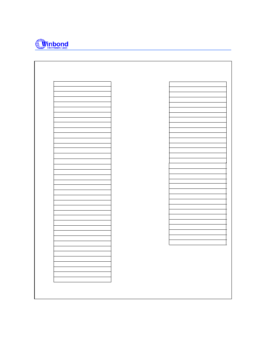
Bottom Boot
[A20-A0]
4KW/8KB Boot Block 0
4KW/8KB Boot Block 1
4KW/8KB Parameter Block 0
4KW/8KB Parameter Block 1
4KW/8KB Parameter Block 2
4KW/8KB Parameter Block 3
4KW/8KB Parameter Block 4
006FFF
006000
005FFF
005000
004FFF
004000
003FFF
003000
002FFF
002000
001FFF
001000
000FFF
000000
07FFFF
078000
077FFF
070000
06FFFF
068000
067FFF
060000
05FFFF
058000
057FFF
050000
04FFFF
048000
047FFF
040000
03FFFF
038000
037FFF
030000
02FFFF
028000
027FFF
020000
01FFFF
018000
017FFF
010000
00FFFF
0EFFFF
0E8000
0E7FFF
0E0000
0DFFFF
0D8000
0D7FFF
0D0000
0CFFFF
0C8000
0C7FFF
0C0000
0BFFFF
0B8000
0B7FFF
0B0000
0AFFFF
0A8000
0A7FFF
0A0000
09FFFF
098000
097FFF
090000
08FFFF
088000
087FFF
080000
32KW/64KB Main Block 15
32KW/64KB Main Block 16
32KW/64KB Main Block 17
32KW/64KB Main Block 18
32KW/64KB Main Block 19
32KW/64KB Main Block 20
32KW/64KB Main Block 21
32KW/64KB Main Block 22
32KW/64KB Main Block 23
32KW/64KB Main Block 24
32KW/64KB Main Block 25
32KW/64KB Main Block 26
32KW/64KB Main Block 27
32KW/64KB Main Block 28
32KW/64KB Main Block 29
32KW/64KB Main Block 30
0F8000
0F7FFF
0F0000
0FFFFF
157FFF
Figure 3.2 Bottom Boot Memory Map

W28J321B/T
Publication Release Date: April 11, 2003
- 11 -
Revision A4
8. BUS OPERATION
The local CPU reads and writes flash memory in-system. All bus cycles to or from the flash memory
conform to standard microprocessor bus cycles.
Read
Information can be read from any block, identifier codes or status register independent of the V
PP
voltage. #RESET can be at V
IH
.
The first task is to write the appropriate read mode command (Read Array, Read Identifier Codes or Read
Status Register) to the CUI. Upon initial device power-up or after exit from reset mode, the device
automatically resets to read array mode. Five control pins dictate the data flow in and out of the
component: #CE, #OE, #WE, #RESET and #WP. #CE and #OE must be driven active to obtain data at
the outputs. #CE is the device selection control, and when active enables the selected memory device.
#OE is the data output (DQ0
- DQ15) control and when active drives the selected memory data onto the
I/O bus. #WE must be at V
IH
, #RESET must be at V
IH
, and #WP must be at V
IL
or V
IH
. Figure 16 illustrates
read cycle.
Output Disable
With #OE at a logic-high level (V
IH
), the device outputs are disabled. Output pins (DQ0
- DQ15) are
placed in a high-impedance state.
Standby
Setting #CE to a logic-high level (V
IH
) deselects the device and places it in standby mode, which
substantially reduces device power consumption. DQ0
- DQ15 outputs are placed in a high
impedance state independent of #OE. If deselected during block erase, full chip erase, word write or
lock-bit configuration, the device continues functioning, and it continues to consume active power until
the operation is completed.
Reset
Setting #RESET to V
IL
initiates the reset mode.
In read modes, setting #RESET at V
IL
deselects the memory, places output drivers in a high-
impedance state and turns off all internal circuits. #RESET must be held low for a minimum of 100 nS.
A delay (t
PHQV
) is required after return from reset until initial memory access outputs are valid. After
this wake-up interval, normal operation is restored. The CUI is reset to read array mode status register
is set to 80H, and all blocks are locked.
During block erase, full chip erase, word write or lock-bit configuration modes, #RESET at V
IL
will
abort the operation. RY/#BY remains low until the reset operation is complete. Memory contents at the
aborted location are no longer valid since the data may be partially erased or written. A delay (t
PHWL
) is
required after #RESET goes to logic-high (V
IH
) before another command can be written.
As with any automated device, it is important to assert #RESET during system reset. When the system
comes out of reset, it expects to read from the flash memory. Automated flash memories provide status
information when accessed during block erase, full chip erase, word write or lock-bit configuration modes.
If a CPU reset occurs with no flash memory reset, proper CPU initialization may not occur because the
flash memory may be providing status information instead of array data. Winbond's flash memories allow
proper CPU initialization following a system reset through the use of the #RESET input. In this application,
#RESET is controlled by the same #RESET signal that resets the system CPU.

W28J321B/T
- 12 -
Read Identifier Codes
The read identifier codes operation outputs the manufacturer code, device code, block lock
configuration codes for each block and the permanent lock configuration code (see Figure 4). Using
the manufacturer and device codes, the system CPU can automatically match the device with its
proper algorithms. The block lock and permanent lock configuration codes identify locked and
unlocked blocks and permanent lock-bit setting.
Reserved for Future Implementation
Boot Block 0 Lock Configuration Code
Reserved for Future Implementation
Boot Block0
Reserved for Future Implementation
Boot Block 1 Lock Configuration Code
Reserved for Future Implementation
Boot Block1
Reserved for Future Implementation
Parameter Block 0 Lock Configuration Code
Reserved for Future Implementation
Parameter Block0
(Parameter Blocks 1 through 4)
Reserved for Future Implementation
Parameter Block 5 Lock Configuration Code
Reserved for Future Implementation
Parameter Block5
Reserved for Future Implementation
Main Block 0 Lock Configuration Code
Reserved for Future Implementation
Mani Block0
(Main Blocks 1 through 61)
Reserved for Future Implementation
OTP Block
Reserved for Future Implementation
Permanent Lock Configuration Code
Main Block 62 Lock Configuration Code
Device Code
Manufacturer Code Mani Block 62
Top Boot
1FFFFF
1FF003
1FF002
1FF001
1FF000
1FEFFF
1FE003
1FE002
1FE001
1FE000
1FDFFF
1FD003
1FD002
1FD001
1FD000
1FCFFF
1F9000
1F8FFF
1F8003
1F8002
1F8001
1F8000
1F7FFF
1F0003
1F0002
1F0001
1F0000
1EFFFF
008000
007FFF
001000
000FFF
000080
00007F
000004
000003
000002
000001
000000
[A20-A0]
Reserved for Future Implementation
Main Block 62 Lock Configuration Code
Reserved for Future Implementation
Main Block 62
Reserved for Future Implementation
Boot Block 1 Lock Configuration Code
Reserved for Future Implementation
Boot Block1
Reserved for Future Implementation
Parameter Block 0 Lock Configuration Code
Reserved for Future Implementation
Parameter Block 0
(Parameter Blocks 1 through 4)
Reserved for Future Implementation
Parameter Block 5 Lock Configuration Code
Reserved for Future Implementation
Parameter Block 5
Reserved for Future Implementation
Main Block 0 Lock Configuration Code
Reserved for Future Implementation
Mani Block0
(Main Blocks 1 through 61)
OTP Block
Reserved for Future Implementation
Permanent Lock Configuration Code
Boot Block 0 Lock Configuration Code
Device Code
Manufacturer Code Boot Block 0
Bottom Boot
1FFFFF
1F8003
1F8002
1F8001
1F8000
1F7FFF
010000
00FFFF
008003
008002
008001
008000
007FFF
007003
007002
007001
007000
006FFF
003000
002FFF
002003
002002
002001
002000
001FFF
001003
001002
001001
001000
000FFF
000080
00007E
000004
000003
000002
000001
000000
[A20-A0]
Figure 4. Device Identifier Code Memory Map

W28J321B/T
Publication Release Date: April 11, 2003
- 13 -
Revision A4
OTP(One Time Program) Block
The OTP block is a special block that can not be erased. The block is divided into two parts. One is a
factory program area where a unique number can be written according to customer requirements in
Winbond factory. This factory program area is "READ ONLY" (Already locked). The other is a
customer program area that can be used by customers. This customer program area can be locked.
After locking, this customer program area is protected permanently.
The OTP block is read in Configuration Read Mode by writing Read Identifier Codes command(90H).
To return to Read Array Mode, write Read Array command(FFH).
The OTP block is programmed by writing OTP Program command(C0H). First write OTP Program
command and then write data with address to the device (See Figure 5).
If OTP program is failed, SR.4(WORD WRITE AND SET LOCK-BIT STATUS) bit is set to "1". And if
this OTP block is locked, SR.1(DEVICE PROTECT STATUS) bit is set to "1" too.
The OTP block is also locked by writing OTP Program command(C0H). First write OTP Program
command and then write data "FFFDH" with address "80H" to the device. Address "80H" of OTP block
is OTP lock information. Bit 0 of address "80H" means factory program area lock status("1" is "NOT
LOCKED", "0" is "LOCKED"). Bit 1 of address "80H" means customer program area lock status. The
OTP lock information can not be cleared, after once it is set.
Customer Program Area
Factory Program Area
OTP Lock
[A20-A0]
00FFF
00085
00084
00081
00080
Customer Program Area Lock
Factory Program Area Lock
Figure 5. OTP Block Address Map

W28J321B/T
- 14 -
Write
Writing commands to the CUI enable reading of device data and identifier codes. They also control
inspection and clearing of the status register. When V
DD
= 2.7V to 3.6V and V
PP
= V
PPH1/2
, the CUI
additionally controls block erase, full chip erase, word write and lock-bit configuration.
The Block Erase command requires appropriate command data and an address within the block to be
erased. The Full Chip Erase command requires appropriate command data and an address within the
device. The Word Write command requires the command and address of the location to be written.
Set Permanent and Block Lock-Bit commands require the command and address within the device
(Permanent Lock) or block within the device (Block Lock) to be locked. The Clear Block Lock-Bits
command requires the command and address within the device.
The CUI does not occupy an addressable memory location. A write occurs when #WE and #CE are
active. The address and data needed to execute a command are latched on the rising edge of #WE or
#CE, whichever occurs first. Standard microprocessor write timings are used.
Figures 17 and 18 illustrate #WE and #CE controlled write operations.
9. COMMAND DEFINITIONS
When V
PP
V
PPLK
, read operations from the status register, identifier codes, or blocks are enabled.
Setting V
PPH1/2
= V
PP
enables successful block erase, full chip erase, word write and lock-bit
configuration operations.
Device operations are selected by writing specific commands into the CUI. Table 3 defines these
commands.
Table 2 Bus Operations (note 1, 2)
MODE #RESET
#CE
#OE
#WE
ADDRESS
V
PP
DQ0
-
15
Read (note 7)
V
IH
V
IL
V
IL
V
IH
X X
DOUT
Output Disable
V
IH
V
IL
V
IH
V
IH
X X
High
Z
Standby V
IH
V
IH
X X
X
X High
Z
Reset (note 3)
V
IL
X X X
X X
High
Z
Read Identifier Codes
(note 7)
V
IH
V
IL
V
IL
V
IH
See
Figure 4, 5
X Note
4
Write (note 5, 6, 7)
V
IH
V
IL
V
IH
V
IL
X X
DIN
Notes:
1. Refer to DC Characteristics. When V
PP
V
PPLK
, memory contents can be read, but not altered.
2. X can be V
IL
or V
IH
for control pins and addresses, and V
PPLK
or V
PPH1/2
for V
PP
. See DC Characteristics for V
PPLK
voltages.
3. #RESET at V
SS
�0.2V ensures the lowest power consumption.
4. See Read Identifier Codes Commands section for details.
5. Command writes involving block erase, full chip erase, word write or lock-bit configuration are reliably executed when V
PP
=
V
PPH1/2
and V
DD
= 2.7V to 3.6V.
6. Refer to Table 3 for valid DIN during a write operation.
7. Never hold #OE low and #WE low at the same timing.

W28J321B/T
Publication Release Date: April 11, 2003
- 15 -
Revision A4
Table 3. Command Definitions
(10)
FIRST BUS CYCLE
SECOND BUS CYCLE
COMMAND
BUS CYCLES
REQ'D.
Oper(1) Addr(2) Data(3) Oper(1) Addr(2) Data(3)
Read Array/Reset
1
Write
X
FFH
Read Identifier Codes
2 (note 4)
Write X 90H Read IA ID
Read Status Register
2
Write X 70H Read X SRD
Clear Status Register 1
Write
X
50H
Block Erase
2 (note 5)
Write X 20H Write
BA D0H
Full Chip Erase
2
Write
X
30H
Write
X
D0H
Word Write
2 (note 5, 6)
Write
X
40H or
10H
Write WA WD
Block Erase and Word Write
Suspend
1 (note 5)
Write
X
B0H
Block Erase and Word Write
Resume
1 (note 5)
Write
X
D0H
Set Block Lock-Bit
2 (note 8)
Write
X
60H
Write
BA
01H
Clear Block Lock-Bits
2 (note 7, 8)
Write
X
60H
Write
X
D0H
Set Permanent Lock-Bit
2 (note 9) Write X
60H Write X F1H
OTP Program
2
Write
X
C0H
Write
OA
OD
Notes:
1. BUS operations are defined in Table 2.
2. X = Any valid address within the device.
IA = Identifier Code Address: see Figure 4.
BA = Address within the block being erased.
WA = Address of memory location to be written.
OA = Address of OTP block to be written: see Figure 5.
3. ID = Data read from identifier codes.
SRD = Data read from status register. See Table 6 for a description of the status register bits.
WD = Data to be written at location WA. Data is latched on the rising edge of #WE or #CE (whichever goes high first).
OD = Data to be written at location OA. Data is latched on the rising edge of #WE or #CE (whichever goes high first).
4. Following the Read Identifier Codes command, read operations access manufacturer, device, block lock configuration and
permanent lock configuration codes. See Read Identifier Codes Command section for details.
5. If #WP is V
IL
, boot blocks are locked without block lock-bits state. If #WP is V
IH
, boot blocks are locked by block lock-bits. The
parameter and main blocks are locked by block lock-bits without #WP state.
6. Either 40H or 10H are recognized by the WSM as the word write setup.
7. The clear block lock-bits operation simultaneously clears all block lock-bits.
8. If the permanent lock-bit is set, Set Block Lock-Bit and Clear Block Lock-Bits commands can not be done.
9. Once the permanent lock-bit is set, permanent lock-bit reset is unable.
10. Commands other than those shown above are reserved by Winbond for future device implementations and should not be
used.

W28J321B/T
- 16 -
Read Array Command
Upon initial device power-up and after exit from reset mode, the device defaults to read array mode.
This operation is also initiated by writing the Read Array command. The device remains enabled for
reads until another command is written. Once the internal WSM has started a block erase, full chip
erase, word write or lock-bit configuration the device will not recognize the Read Array command until
the WSM completes its operation unless the WSM is suspended via an Erase Suspend or Word Write
Suspend command. The Read Array command functions independently of the V
PP
voltage and
#RESET can be V
IH
.
Read Identifier Codes Command
The identifier code operation is initiated by writing the Read Identifier Codes command. Following the
command write, read cycles from addresses shown in Figure 4 retrieve the manufacturer, device,
block lock configuration and permanent lock configuration codes (see Table 4 for identifier code
values). To terminate the operation, write another valid command. Like the Read Array command, the
Read Identifier Codes command functions independently of the V
PP
voltage and #RESET can be V
IH
.
Following the Read Identifier Codes command, the following information can be read:
Table 4. Identifier Codes
CODE
ADDRESS(2)
[A20
-
A0]
DATA(3)
[DQ15
-
DQ0]
Manufacture Code
00000H
00B0H
Top Boot
00E2H
Device Code
Bottom Boot
00001H
00E3H
DQ0 = 0
DQ0 = 1
Block Lock Configuration
� Block is Unlocked
� Block is Locked
� Reserved for Future Use
BA(1)+2
DQ1
-
7
DQ0 = 0
DQ0 = 1
Permanent Lock Configuration
� Device is Unlocked
� Device is Locked ed
� Reserved for Future Use
00003H
DQ1
-
7
Note: BA selects the specific block lock configuration code to be read. See Figure 4 for the device identifier code memory map.
Read Status Register Command
The status register may be read to determine when a block erase, full chip erase, word write or lock-
bit configuration is complete and whether the operation completed successfully. It may be read at any
time by writing the Read Status Register command. After writing this command, all subsequent read
operations output data from the status register until another valid command is written. The status
register contents are latched on the falling edge of #OE or #CE, whichever occurs last. #OE or #CE
must toggle to V
IH
before further reads to update the status register latch. The Read Status Register
command functions independently of the V
PP
voltage. #RESET can be V
IH
.

W28J321B/T
Publication Release Date: April 11, 2003
- 17 -
Revision A4
Clear Status Register Command
Status register bits SR.5, SR.4, SR.3 or SR.1 are set to "1"s by the WSM and can only be reset by the
Clear Status Register command. These bits indicate various failure conditions (see Table 6). By
allowing system software to reset these bits, several operations (such as cumulatively erasing multiple
blocks or writing several words in sequence) may be performed. The status register may be polled to
determine if an error occurred during the sequence.
To clear the status register, the Clear Status Register command (50H) is written. It functions
independently of the applied V
PP
voltage. #RESET can be V
IH
. This command is not functional during
block erase or word write suspend modes.
Block Erase Command
Erase is executed one block at a time and initiated by a two-cycle command. A block erase setup is
first written, followed by an block erase confirm. This command sequence requires appropriate
sequencing and an address within the block to be erased (all bits within the block being set to "1").
Block preconditioning, erase, and verify are handled internally by the WSM (invisible to the system).
After the two-cycle block erase sequence is written, the device automatically outputs status register
data when read (see Figure 6). The CPU can detect block erase completion by analyzing the status
register bit SR.7.
When the block erase is complete, status register bit SR.5 should be checked. If a block erase error is
detected, the status register should be cleared before system software attempts corrective actions.
The CUI remains in read status register mode until a new command is issued.
This two-step command sequence of set-up followed by execution ensures that block contents are not
accidentally erased. An invalid Block Erase command sequence will result in both status register bits
SR.4 and SR.5 being set to "1". Also, reliable block erasure can only occur when V
DD
= 2.7V to 3.6V
and V
PP
= V
PPH1/2
. In the absence of this high voltage, block contents are protected against erasure. If
block erase is attempted while V
PP
V
PPLK
, SR.3 and SR.5 will be set to "1". Successful block erase
requires for boot blocks that #WP is V
IH
and the corresponding block lock-bit be cleared. In parameter
and main blocks case, it must be cleared the corresponding block lock-bit. If block erase is attempted
when the excepting above conditions, SR.1 and SR.5 will be set to "1".
Full Chip Erase Command
This command followed by a confirm command erases all of the unlocked blocks. A full chip erase
setup (30H) is first written, followed by a full chip erase confirm (D0H). After a confirm command is
written, device erases the all unlocked blocks block by block. This command sequence requires
appropriate sequencing. Block preconditioning, erase and verify are handled internally by the WSM
(invisible to the system). After the two-cycle full chip erase sequence is written, the device
automatically outputs status register data when can be read (refer to Figure 7). The CPU can detect
full chip erase completion by analyzing the output data of the status register bit SR.7.
When the full chip erase is complete, status register bit SR.5 should be checked. If erase error is
detected, the status register should be cleared before system software attempts corrective actions.
The CUI remains in read status register mode until a new command is issued. If error is detected on a
block during full chip erase operation, WSM stops erasing. Full chip erase operation start from lower
address block, finish the higher address block. Full chip erase can not be suspended. This two-step
command sequence of set-up followed by execution ensures that block contents are not accidentally
erased. An invalid Full Chip Erase command sequence will result in both status register bits SR.4 and

W28J321B/T
- 18 -
SR.5 being set to "1". Also, reliable full chip erasure can only occur when V
DD
= 2.7V to 3.6V and V
PP
=
V
PPH1/2
. In the absence of this high voltage, block contents are protected against erasure. If full chip
erase is attempted while V
PP
V
PPLK
, SR.3 and SR.5 will be set to "1". Successful full chip erase
requires for boot blocks that #WP is V
IH
and the corresponding block lock-bit be cleared. In parameter
and main blocks case, it must clear the corresponding block lock-bit. If all blocks are locked, SR.1 and
SR.5 will be set to "1".
Word Write Command
Word write is executed by a two-cycle command sequence. Word write setup (standard 40H or
alternate 10H) is written, followed by a second write that specifies the address and data (latched on
the rising edge of #WE). The WSM then takes over; controlling the word write and write verify
algorithms internally. After the word write sequence is written, the device automatically outputs status
register data when read (see Figure 8). The CPU can detect the completion of the word write event by
analyzing the status register bit SR.7.
When word write is complete, status register bit SR.4 should be checked. If word write error is
detected, the status register should be cleared. The internal WSM verify only detects errors for "1"s
that do not successfully write to "0"s. The CUI remains in read status register mode until it receives
another command.
Reliable word writes can only occur when V
DD
= 2.7V to 3.6V and V
PP
= V
PPH1/2
. In the absence of this
high voltage, memory contents are protected against word writes. If word write is attempted while V
PP
V
PPLK
, status register bits SR.3 and SR.4 will be set to "1". Successful word write for boot blocks
requires that #WP = V
IH
and the corresponding block lock-bit be cleared. In parameter and main
blocks case, the corresponding block lock-bit must be cleared. If word write is attempted under these
conditions, SR.1 and SR.4 will be set to "1".
Block Erase Suspend Command
The Block Erase Suspend command allows block-erase interruption to read or word write data in
another block of memory. Once the block erase process starts, writing the Block Erase Suspend
command requests that the WSM suspend the block erase sequence at a predetermined point in the
algorithm. The device outputs status register data when read after the Block Erase Suspend
command is written. Polling status register bits SR.7 and SR.6 can determine when the block erase
operation has been suspended (both will be set to "1"). The period t
WHR12
defines the block erase
suspend latency.
When Block Erase Suspend command writes to the CUI, if block erase is finished, the device is
placed in read array mode. Therefore, after Block Erase Suspend command writes to the CUI, Read
Status Register command (70H) has to write to CUI, and then status register bit SR.6 should be
checked to confirm that the device is in suspend mode. At this point, a Read Array command can be
written to read data from blocks other than that which is suspended.
To program data in other blocks, a Word Write command sequence can also be issued during erase
suspend. Using the Word Write Suspend command (reference the Word Write Suspend Command
subsection), a word write operation can also be suspended. During a word write operation with block
erase suspended, status register bit SR.7 will return to "0". However, SR.6 will remain "1" to indicate
block erase suspend status.
The only other valid commands while block erase is suspended are Read Status Register and Block
Erase Resume. After a Block Erase Resume command is written to the flash memory, the WSM will
continue the block erase process. Status register bits SR.6 and SR.7 will automatically clear. After the
Erase Resume command is written, the device automatically outputs status register data when read

W28J321B/T
Publication Release Date: April 11, 2003
- 19 -
Revision A4
(see Figure 9). V
PP
must remain at V
PPH1/2
(the same V
PP
level used for block erase) while block erase
is suspended. #RESET must also remain at V
IH
. #WP must also remain at V
IL
or V
IH
(the same #WP
level used for block erase). Block erase cannot resume until word write operations initiated during
block erase suspend have completed.
Word Write Suspend Command
The Word Write Suspend command allows word write interruption to read data in other flash memory
locations. Once the word write process starts, sending the Word Write Suspend command causes that
the WSM to suspend the Word write sequence at a predetermined point in the algorithm. The device
continues to output status register data when read after the Word Write Suspend command is written.
Polling status register bits SR.7 and SR.2 can determine when the word write operation has been
suspended (both will be set to "1"). The period t
WHR11
defines the word write suspend latency
parameters.
When Word Write Suspend command write to the CUI, if word write was finished, the device places
read array mode. Therefore, after Word Write Suspend command write to the CUI, Read Status
Register command (70H) has to write to CUI, then status register bit SR.2 should be checked to
confirm the device is in suspend mode.
At this point, a Read Array command can be written to read data from locations other than that which
is suspended. The only other valid commands while word write is suspended are Read Status
Register and Word Write Resume. After Word Write Resume command is written to the flash memory,
the WSM will continue the word write process. Status register bits SR.2 and SR.7 will automatically
clear. After the Word Write Resume command is written, the device automatically outputs status
register data when read (see Figure 10). V
PP
must remain at V
PPH1/2
(the same V
PP
level used for word
write) while in word write suspend mode. #RESET must also remain at V
IH
. #WP must also remain at
V
IL
or V
IH
(the same #WP level used for word write).
If the period from Word Write Resume command write to Word Write Suspend command write is too
short, it can be repeated, and the write time will be prolonged.
Set Block and Permanent Lock-Bit Commands
A flexible block locking and unlocking scheme is enabled via a combination of block lock-bits, a
permanent lock-bit and #WP pin. The block lock-bits and #WP pin gates program and erase
operations while the permanent lock-bit gates block-lock bit modification. With the permanent lock-bit
not set, individual block lock-bits can be set using the Set Block Lock-Bit command. The Set
Permanent Lock-Bit command sets, sets the permanent lock-bit. After the permanent lock-bit is set,
block lock-bits and locked block contents cannot altered. Refer to Table 5 for a summary of hardware
and software write protection options.
Set block lock-bit and permanent lock-bit are executed by a two-cycle command sequence. The set
block or permanent lock-bit setup along with appropriate block or device address is written followed by
either the set block lock-bit confirm (and an address within the block to be locked) or the set
permanent lock-bit confirm (and any device address). The WSM then executes the set lock-bit
algorithm. After the sequence is written, the device automatically outputs status register data when
read (see Figure 11). The CPU can detect the completion of the set lock-bit event by analyzing the
status register bit SR.7.
When the set lock-bit operation is complete, status register bit SR.4 should be checked. If an error is
detected, the status register should be cleared. The CUI will remain in read status register mode until
a new command is issued.

W28J321B/T
- 20 -
This two-step sequence of set-up followed by execution ensures that lock-bits are not accidentally set.
An invalid Set Block or Permanent Lock-Bit command will result in status register bits SR.4 and SR.5
being set to "1". Also, reliable operations occur only when V
DD
= 2.7V to 3.6V and V
PP
= V
PPH1/2
. In the
absence of this high voltage, lock-bit contents are protected against alteration.
A successful set block lock-bit operation requires that the permanent lock-bit be cleared. If it is
attempted with the permanent lock-bit set, SR.1 and SR.4 will be set to "1" and the operation will fail.
Clear Block Lock-Bits Command
All set block lock-bits are cleared in parallel via the Clear Block Lock-Bits command. If the permanent
lock-bit is not set, block lock-bits can be cleared using only the Clear Block Lock-Bits command. If the
permanent lock-bit is set, block lock-bits cannot cleared. See Table 5 for a summary of hardware and
software write protection options.
Clear block lock-bits operation is executed by a two-cycle command sequence. A clear block lock-bits
setup is first written. After the command is written, the device automatically outputs status register
data when read (see Figure 12). The CPU can detect completion of the clear block lock-bits event by
sending the status register bit SR.7.
When the operation is complete, status register bit SR.5 should be checked. If a clear block lock-bit
error is detected, the status register should be cleared. The CUI will remain in read status register
mode until another command is issued.
This two-step sequence of set-up followed by execution ensures that block lock-bits are not
accidentally cleared. An invalid Clear Block Lock-Bits command sequence will result in status register
bits SR.4 and SR.5 being set to "1". Also, a reliable clear block lock-bits operation can only occur
when V
DD
= 2.7V to 3.6V and V
PP
= V
PPH1/2
. If a clear block lock-bits operation is attempted while V
PP
V
PPLK
, SR.3 and SR.5 will be set to "1". In the absence of this high voltage, the block lock-bits content
are protected against alteration. A successful clear block lock-bits operation requires that the
permanent lock-bit is not set. If it is attempted with the permanent lock-bit set, SR.1 and SR.5 will be
set to "1" and the operation will fail.
If a clear block lock-bits operation is aborted due to V
PP
or V
DD
transitioning out of valid range or
#RESET is toggled, block lock-bit values are left in an undetermined state. A repeat of clear block
lock-bits is required to initialize block lock-bit contents to known values. Once the permanent lock-bit
is set, it cannot be cleared.
OTP Program Command
OTP program is executed by a two-cycle command sequence. OTP program command(C0H) is
written, followed by a second write cycle that specifies the address and data (latched on the rising
edge of #WE). The WSM then takes over, controlling the OTP program and program verify algorithms
internally. After the OTP program command sequence is completed, the device automatically outputs
status register data when read (see Figure 13). The CPU can detect the completion of the OTP
program by analyzing the status register bit SR.7.
When OTP program is completed, status register bit SR.4 should be checked. If OTP program error is
detected, the status register should be cleared. The internal WSM verify only detects errors for "1"s
that do not successfully program to "0"s. The CUI remains in read status register mode until it receives
other commands.
Reliable OTP program can be executed only when V
DD
= 2.7V to 3.6V and V
PP
= V
PPH1/2
. In the
absence of this voltage, memory contents are protected against OTP programs. If OTP program is

W28J321B/T
Publication Release Date: April 11, 2003
- 21 -
Revision A4
attempted while V
PP
V
PPLK
, status register bits SR.3 and SR.4 is set to "1". If OTP write is attempted
when the OTP Lock-bit is set, SR.1 and SR.4 is set to "1".
Block Locking by the #WP
This Boot Block Flash memory architecture features two hardware-lockable boot blocks so that the
kernel code for the system can be kept secure while other blocks are programmed or erased as
necessary. The lockable two boot blocks are locked when #WP = V
IL
; any program or erase operation
to a locked block will result in an error, which will be reflected in the status register. For top
configuration, the top two boot blocks are lockable. For the bottom configuration, the bottom two boot
blocks are lockable. If #WP is V
IH
and block lock-bit is not set, boot block can be programmed or
erased normally (Unless V
PP
is below V
PPLK
). #WP is valid only two boot blocks, other blocks are not
affected.
Table 5. Write Protection Alternatives
OPERATION
V
PP
#RESET
PERMANENT
LOCK-BIT
BLOCK
LOCK-BIT
#WP EFFECT
V
PPLK
X
X
X
X
All Blocks Locked.
V
IL
X
X
X
All Blocks Locked.
V
IL
2 Boot Blocks Locked.
0
V
IH
Block Erase and Word Write Enabled.
V
IL
Block Erase and Word Write Disabled.
Block Erase
or Word Write > V
PPLK
V
IH
X
1
V
IH
Block Erase and Word Write Disabled.
V
PPLK
X
X
X
X
All Blocks Locked.
V
IL
X
X
X
All Blocks Locked.
V
IL
All Unlocked Blocks are Erased.
2 Boot Blocks and Locked Blocks are NOT
Erased.
Full Chip
Erase
> V
PPLK
V
IH
X X
V
IH
All Unlocked Blocks are Erased.
Locked Blocks are NOT Erased.
V
PPLK
X
X
X
X
Set Block Lock-Bit Disabled.
V
IL
X
X
X
Set Block Lock-Bit Disabled.
0
X
X
Set Block Lock-Bit Enabled.
Set Block
Lock-Bit
> V
PPLK
V
IH
1
X
X
Set Block Lock-Bit Disabled.
V
PPLK
X
X
X
X
Clear Block Lock-Bits Disabled.
V
IL
X
X
X
Clear Block Lock-Bits Disabled.
0
X
X
Clear Block Lock-Bits Enabled.
Clear Block
Lock-Bits
> V
PPLK
V
IH
1
X
X
Clear Block Lock-Bits Disable.
V
PPLK
X
X
X
X
Set Permanent Lock-Bit Disabled.
V
IL
X
X
X
Set Permanent Lock-Bit Disabled.
Set
Permanent
Lock-Bit
> V
PPLK
V
IH
X
X
X
Set Permanent Lock-Bit Enabled.

W28J321B/T
- 22 -
Table 6. Status Register Definition
WSMS BESS
ECBLBS
WWSLBS
VPPS WWSS DPS R
7 6 5 4 3 2 1 0
SR.7 = WRITE STATE MACHINE STATUS (WSMS)
1 = Ready
0 = Busy
SR.6 = BLOCK ERASE SUSPEND STATUS (BESS)
1 = Block Erase Suspended
0 = Block Erase in Progress/Completed
SR.5 = ERASE AND CLEAR BLOCK LOCK-BITS STATUS
(ECBLBS)
1 = Error in Block Erase, Full Chip Erase or Clear Block
Lock-Bits
0 = Successful Block Erase, Full Chip Erase or Clear
Block Lock-Bits
SR.4 = WORD WRITE AND SET LOCK-BIT STATUS
(WWSLBS)
1 = Error in Word Write or Set Block/Permanent Lock-Bit
0 = Successful Word Write or Set Block/Permanent Lock-
Bit
SR.3 = V
PP
STATUS (VPPS)
1 = V
PP
Low Detect, Operation Abort
0 = V
PP
OK
SR.2 = WORD WRITE SUSPEND STATUS (WWSS)
1 = Word Write Suspended
0 = Word Write in Progress/Completed
SR.1 = DEVICE PROTECT STATUS (DPS)
1 = Block Lock-Bit, Permanent Lock-Bit and/or #WP Lock
Detected, Operation Abort
0 = Unlock
SR.0 = RESERVED FOR FUTURE ENHANCEMENTS (R)
Notes:
Check SR.7 to determine block erase, full chip erase, word
write or lock-bit configuration completion. SR.6-0 are invalid
while SR.7 = "0".
If both SR.5 and SR.4 are "1"s after a block erase, full chip
erase or lock-bit configuration attempt, an improper
command sequence was entered.
SR.3 does not provide a continuous indication of V
PP
level.
The WSM interrogates and indicates the V
PP
level only after
Block Erase, Full Chip Erase, Word Write or Lock-Bit
Configuration command sequences. SR.3 is not
guaranteed to reports accurate feedback only when V
PP
V
PPH1/2
.
SR.1 does not provide a continuous indication of
permanent and block lock-bit and #WP values. The WSM
interrogates the permanent lock-bit, block lock-bit and #WP
only after Block Erase, Full Chip Erase, Word Write or
Lock-Bit Configuration command sequences. It informs the
system, depending on the attempted operation, if the block
lock-bit is set, permanent lock-bit is set and/or #WP is
V
IL
.
Reading the block lock and permanent lock configuration
codes after writing the Read Identifier Codes command
indicates permanent and block lock-bit status.
SR.0 is reserved for future use and should be masked out
when polling the status register.

W28J321B/T
Publication Release Date: April 11, 2003
- 23 -
Revision A4
Bus Operation Command
Comments
Write
Read Status
Register
Data = 70H
Addr = X
Read
Status Register Data
Standby
Check SR.7
1=WSM Ready
0=WSM Busy
Write Erase
Setup
Data = 20H
Addr = X
Write
Erase
Confirm
Data = D0H
Addr = Within Block to be
Erased
Read
Status Register Data
Standby
Check SR.7
1 = WSM Ready
0 = WSM Busy
Repeat for subsequent block erasures. Full status check
can be done after each block erase or after a sequence of
block erasures. Write FFH after the last operation to place
device in read array mode.
Start
Write 70H
SR.7=
Write 20H
Read Status
Register
SR.7=
Full Status
Check if Desired
Block Erase
Complete
Read Status
Register
Write D0H,
Block Address
1
0
1
0
Suspend Block
Suspend
Block Erase
Erase Loop
No
Yes
Full STATUS CHECK PROCEDURE
Read Status Register
Data(See Above)
SR.3=
SR.1=
SR.4,5=
SR.5=
Block Erase Sucessfully
0
0
0
0
1
1
1
1
Vpp Range Error
Device Protect Error
Command Sequence
Block Erase Error
Error
Bus Operation Command
Comments
Standby
Check SR.3
1 =
V
PP
Error Detect
Standby
Check SR.1
1 = Device Protect Detect
Standby
Check SR.4, 5
Both 1 = Command
Sequence Error
Standby
Check SR.5
1 = Block Erase Error
SR.5, SR.4, SR.3 and SR.1 are only cleared by the Clear
Status Register Command in cases where multiple blocks
are erased before full status is checked.
If error is detected, clear the Status Register before
attempting retry or other error recovery.
Figure 6. Automated Block Erase Flowchart

W28J321B/T
- 24 -
Bus Operation Command
Comments
Write
Read Status
Register
Data = 70H
Addr = X
Read
Status Register Data
Standby
Check SR.7
1 = WSM Ready
0 = WSM Busy
Write
Full Chip
Erase
Setup
Data = 30H
Addr = X
Write
Full Chip
Erase
Confirm
Data = D0H
Addr = X
Read
Status Register Data
Standby
Check SR.7
1 = WSM Ready
0 = WSM Busy
Full status check can be done after each full chip erase.
Write FFH after the last operation to place device in read
array mode.
Start
Write 70H
SR.7=
Write 30H
Read Status
Register
SR.7=
Full Status
Check if Desired
Full Chip Erase
Complete
Read Status
Register
Write D0H
1
0
1
0
Full STATUS CHECK PROCEDURE
Read Status Register
Data(See Above)
SR.3=
SR.1=
SR.4,5=
SR.5=
Full Chip Erase
0
0
0
0
1
1
1
1
Vpp Range Error
Device Protect Error
Command Sequence
Full Chip Erase Error
Error
Successfully
Bus Operation Command
Comments
Standby
Check SR.3
1 =
V
PP
Error Detect
Standby
Check SR.1
1 = Device Protect Detect
(All Blocks are locked)
Standby
Check SR.4, 5
Both 1 = Command
Sequence Error
Standby
Check SR.5
1 = Full Chip Erase Error
SR.5, SR.4, SR.3 and SR.1 are only cleared by the Clear
Status Register Command in cases where multiple blocks
are erased before full status is checked.
If error is detected, clear the Status Register before
attempting retry or other error recovery.
Figure 7. Automated Full Chip Erase Flowchart
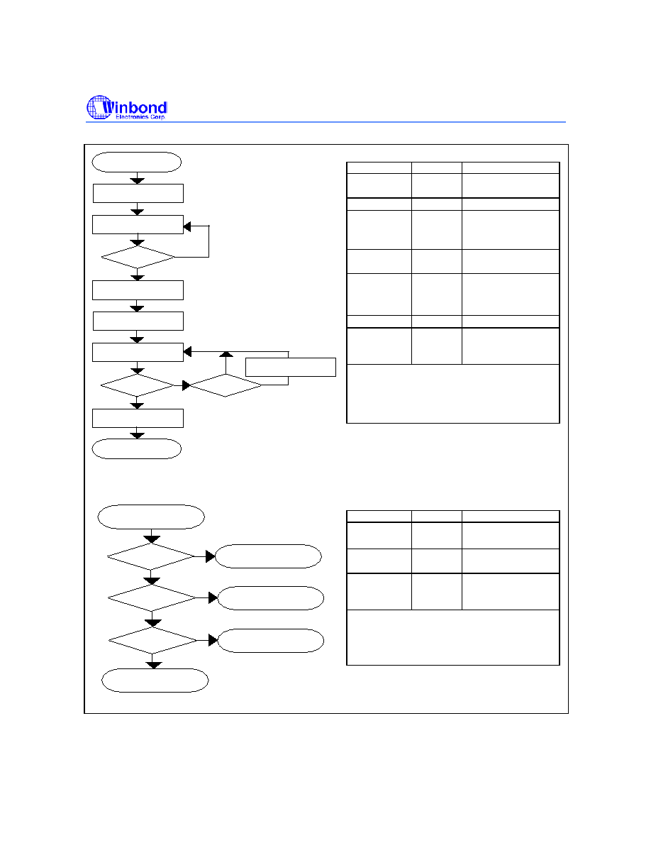
W28J321B/T
Publication Release Date: April 11, 2003
- 25 -
Revision A4
Bus Operation Command
Comments
Write
Read Status
Register
Data = 70H
Addr = X
Read
Status Register Data
Standby
Check SR.7
1 = WSM Ready
0 = WSM Busy
Write
Setup Word
Write
Data = 40H or 10H
Addr = X
Write Word
Write
Data = Data to Be
Written
Addr = Location to Be
written
Read
Status Register Data
Standby
Check SR.7
1 = WSM Ready
0 = WSM Busy
Repeat for subsequent word writes.
SR full status check can be done after each word write,
or after a sequence of word writes.
Write FFH after the last word write operation to place
device in read array mode.
Start
Write 70H
SR.7=
Write 40H or 10H
Read Status
Register
SR.7=
Full Status
Check if Desired
Word/Byte Write
Complete
Read Status
Register
Write Word/Byte
1
0
1
Data and Adddress
Suspend
Word/Byte
Write Loop
No
Yes
Write
Suspend Word/Byte
0
Full STATUS CHECK PROCEDURE
Read Status Register
Data(See Above)
SR.3=
SR.1=
SR.4=
0
0
0
1
1
1
Vpp Range Error
Device Protect Error
Word/Byte Write Error
Word/Byte Write
Successfully
Bus Operation Command
Comments
Standby
Check SR.3
1 =
V
PP
Error Detect
Standby
Check SR.1
1 = Device Protect Detect
Standby
Check SR.4
1 = Data Write Error
SR.4, SR.3 and SR.1 are only cleared by the Clear
Status Register command in cases where multiple
locations are written before full status is checked.
If error is detected, clear the Status Register before
attempting retry or other error recovery.
Figure 8. Automated Word Write Flowchart

W28J321B/T
- 26 -
Start
Write B0H
Read Status
Register
SR.7=
1
0
SR.6=
0
Block Erase
Complete
1
Read or
Word/Byte
Write?
No
Yes
Done?
Write D0H
Block Erase
Resumed
Write FFH
Read Array Data
Word/Byte write
Wore/Byte Write Loop
Read
Read Array Data
Bus Operation Command
Comments
Write
Erase
Suspend
Data = B0H
Addr = X
Read
Status Register Data
Addr = X
Standby
Check SR.7
1 = WSM Ready
0 = WSM Busy
Standby
Check SR.6
1 = Block Erase
Suspended
0 = Block Erase
Completed
Write
Erase
Resume
Data = D0H
Addr = X
Figure 9. Block Erase Suspend/Resume Flowchart

W28J321B/T
Publication Release Date: April 11, 2003
- 27 -
Revision A4
Start
Write B0H
Read Status
Register
SR.7=
1
0
SR.2=
0
Word/Byte Write
Completed
1
Yes
Done
Write D0H
Word/Byte Write
Resumed
Write FFH
Read Array Data
Write FFH
Read Array Data
Reading
No
Bus Operation Command
Comments
Write
Word Write
Suspend
Data = B0H
Addr = X
Read
Status Register Data
Addr = X
Standby
Check SR.7
1 = WSM Ready
0 = WSM Busy
Standby
Check SR.2
1 = Word Write Suspended
0 = Word Write Completed
Write Read
Array
Data = FFH
Addr = X
Read
Read Array locations other
than that being written.
Write
Word Write
Resume
Data = D0H
Addr = X
Figure 10. Word Write Suspend/Resume Flowchart

W28J321B/T
- 28 -
Bus Operation
Command
Comments
Write
Read Status
Register
Data = 70H
Addr = X
Read
Status Register Data
Standby
Check SR.7
1 = WSM Ready
0 = WSM Busy
Write
Set Block/
Permanent
Lock-Bit Setup
Data = 60H
Addr = X
Write
Set Block or
Permanent
Lock-Bit
Confirm
Data = 01H(Block),
F1H(Permanent)
Addr = Block
Address(Block),
Device Address(Permanent)
Read
Status Register Data
Standby
Check SR.7
1 = WSM Ready
0 = WSM Busy
Repeat for subsequent lock-bit set operations.
Full status check can be done after each lock-bit set operation
or after a sequence of lock-bit set operations.
Write FFH after the last lock-bit set operation to place device in
read array mode.
Start
Write 70H
SR.7=
Write 60H
Read Status
Register
SR.7=
Full Status
Check if Desired
Set Lock-Bit
Complete
Read Status
Register
Write 01H/F1H
1
0
1
0
Block/Device Address
Full STATUS CHECK PROCEDURE
Read Status Register
Data(See Above)
SR.3=
SR.1=
SR.4,5=
SR.4=
Set Lock-Bit
Successfully
0
0
0
0
1
1
1
1
Vpp Range Error
Device Protect Error
Command Sequence
Set Lock-Bit Error
Error
Bus Operation Command
Comments
Standby
Check SR.3
1 =
V
PP
Error Detect
Standby
Check SR.1
1 = Device Protect Detect
Permanent Lock-Bit is Set
(Set Block Lock-Bit Operation)
Standby
Check SR.4, 5
Both 1 = Command Sequence
Error
Standby
Check SR.4
1 = Set Lock-Bit Error
SR.5, SR.4, SR.3 and SR.1 are only cleared by the Clear
Status Register command in cases where multiple lock-bits are
set before full status is checked.
If error is detected, clear the Status Register before attempting
retry or other error recovery.
Figure 11. Set Block and Permanent Lock-Bit Flowchart

W28J321B/T
Publication Release Date: April 11, 2003
- 29 -
Revision A4
Bus Operation
Command
Comments
Write
Read Status
Register
Data = 70H
Addr = X
Read
Status Register Data
Standby
Check SR.7
1 = WSM Ready
0 = WSM Busy
Write
Clear Block
Lock-Bits
Setup
Data = 60H
Addr = X
Write
Clear Block
Lock-Bits
Confirm
Data = D0H
Addr = X
Read
Status Register Data
Standby
Check SR.7
1 = WSM Ready
0 = WSM Busy
Write FFH after the Clear Block Lock-Bits operation to
place device in read array mode.
Start
Write 70H
SR.7=
Write 60H
Read Status
Register
SR.7=
Full Status
Check if Desired
Clear Block Lock-Bits
Complete
Read Status
Register
Write D0H
1
0
1
0
Full STATUS CHECK PROCEDURE
Read Status Register
Data(See Above)
SR.3=
SR.1=
SR.4,5=
SR.5=
Clear Block Lock-Bits
0
0
0
0
1
1
1
1
Vpp Range Error
Device Protect Error
Command Sequence
Clear Block Lock-Bits Error
Error
Successfully
Bus Operation Command
Comments
Standby
Check SR.3
1 =
V
PP
Error Detect
Standby
Check SR.1
1 = Device Protect Detect
Permanent Lock-Bit is Set
Standby
Check SR.4, 5
Both 1= Command
Sequence Error
Standby
Check SR.5
1 = Clear Block Lock-Bits
Error
SR.5, SR.4, SR.3 and SR.1 are only cleared by the Clear
Status Register command. If error is detected, clear the
Status Register before attempting retry or other error
recovery.
Figure 12. Clear Block Lock-Bits Flowchart
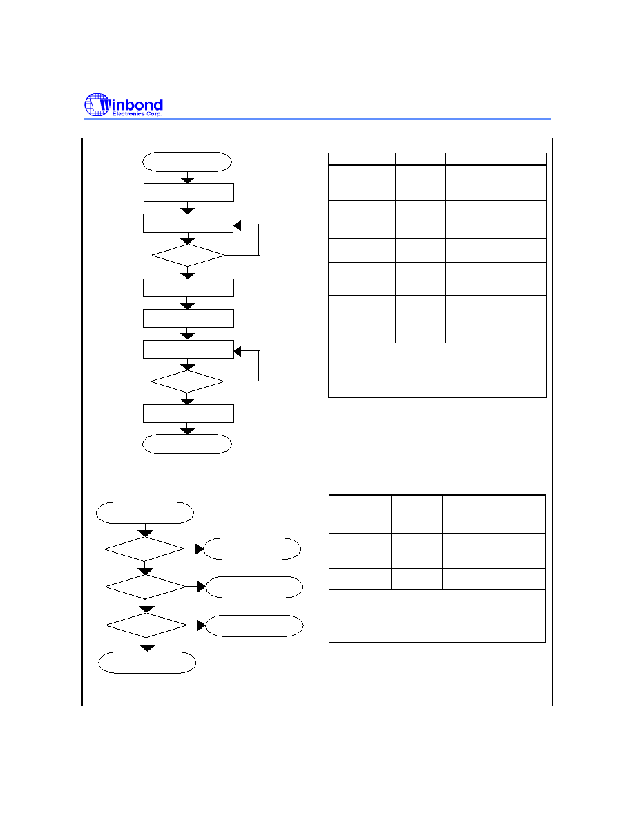
W28J321B/T
- 30 -
Bus Operation Command
Comments
Write
Read Status
Register
Data = 70H
Addr = X
Read
Status Register Data
Standby
Check SR.7
1 = WSM Ready
0 = WSM Busy
Write
Setup OTP
Program
Data = C0H
Addr = X
Write
OTP
Program
Data = Data to Be Written
Addr = Location to Be
Written
Read
Status Register Data
Standby
Check SR.7
1 = WSM Ready
0 = WSM Busy
Repeat for subsequent OTP programs.
SR full status check can be done after each OTP program,
or after a sequence of OTP programs.
Write FFH after the last OTP program operation to place
device in read array mode.
Start
Write 70H
SR.7=
Write C0H
Read Status
Register
SR.7=
Full Status
Check if Desired
OTP Program
Complete
Read Status
Register
Write Data
and Address
1
0
1
0
Full STATUS CHECK PROCEDURE
Read Status Register
Data(See Above)
SR.3=
SR.1=
SR.4=
0
0
0
1
1
1
Vpp Range Error
Device Protect Error
OTP Program
Sucessfully
OTP Program
Sucessfully
Bus Operation Command
Comments
Standby
Check SR.3
1 =
V
PP
Error Detect
Standby
Check SR.1
1 = Device Protect Detect
Standby
Check SR.4
1 = Data Write Error
SR.4, SR.3 and SR.1 are only cleared by the Clear Status
Register command in cases where multiple locations are
written before full status is checked.
If error is detected, clear the Status Register before
attempting retry or other error recovery.
Figure 13. Automated OTP Program Flowchart

W28J321B/T
Publication Release Date: April 11, 2003
- 31 -
Revision A4
10. DESIGN CONSIDERATIONS
Three-Line Output Control
This device will often be used in large memory arrays. Winbond provides three control inputs to
accommodate multiple memory connections. Three-line control provides for:
a. Lowest possible memory power dissipation.
b. Complete assurance that data bus contention will not occur.
To use these control inputs efficiently, an address decoder should enable #CE while #OE should be
connected to all memory devices and the system's READ control line. This assures that only selected
memory devices have active outputs while deselected memory devices are in standby mode. #RESET
should be connected to the system POWERGOOD signal to prevent unintended writes during system
power transitions. POWERGOOD should also toggle during system reset.
Power Supply Decoupling
Flash memory power switching characteristics require careful device decoupling. System designers
are interested in three supply current issues; standby current levels, active current levels and transient
peaks produced by falling and rising edges of #CE and #OE. Transient current magnitudes depend on
the device outputs' capacitive and inductive loading. Two-line control and proper decoupling capacitor
selection will suppress transient voltage peaks.
Each device should have a 0.1
�F ceramic capacitor connected between V
DD
and V
SS
and between
V
PP
and V
SS
. These high frequency, low inductance capacitors should be placed as close as possible
to package leads. Additionally, for every eight devices, a 4.7
�F electrolytic capacitor should be placed
at the array's power supply connection between V
DD
and V
SS
. The bulk capacitor will overcome
voltage drops caused by PC board trace inductance.
V
PP
Trace on Printed Circuit Boards
Updating flash memories that reside in the target system requires that the printed circuit board
designer pay attention to the V
PP
power supply trace. The V
PP
pin supplies the memory cell current for
Word writing and block erasing. Use similar trace widths and layout considerations given to the V
DD
power bus. Adequate V
PP
supply traces and decoupling will decrease V
PP
voltage spikes and
overshoots.
V
DD
, V
PP
, #RESET Transitions
Block erase, full chip erase, word write and lock-bit configuration are not guaranteed if V
PP
falls
outside of a valid V
PPH1/2
range, V
DD
falls outside of a valid 2.7V to 3.6V range, or #RESET
V
IH
. If V
PP
error is detected, status register bit SR.3 is set to "1" along with SR.4 or SR.5, depending on the
attempted operation. If #RESET transitions to V
IL
during block erase, full chip erase, word write or
lock-bit configuration, SR.7 will remain "0" until the reset operation is complete. Then, the operation
will abort and the device will enter reset mode. The aborted operation may leave data partially altered.
Therefore, the command sequence must be repeated after normal operation is restored. Device
power-off or #RESET transitions to V
IL
clear the status register.
The CUI latches commands issued by system software and is not altered by V
PP
or #CE transitions or
WSM actions. Its state is read array mode upon power-up, after exit from reset mode or after V
DD
transitions below V
LKO
.

W28J321B/T
- 32 -
Power-up/Down Protection
The device is designed to offer protection against accidental block erase, full chip erase, word write or
lock-bit configuration during power transitions. Upon power-up, the device is indifferent as to which
power supply (V
PP
or V
DD
) powers-up first. Internal circuitry resets the CUI to read array mode at
power-up.
A system designer must guard against spurious writes for V
DD
voltages above V
LKO
when V
PP
is active.
Since both #WE and #CE must be low for a command write, driving either to V
IH
will inhibit writes. The
CUI's two-step command sequence architecture provides added level of protection against data
alteration.
In-system block lock and unlock capability prevents inadvertent data alteration. The device is disabled
while #RESET = V
IL
regardless of its control inputs state.
Power Dissipation
When designing portable systems, designers must consider battery power consumption not only
during device operation, but also for data retention during system idle time. Flash memory's
nonvolatility increases usable battery life because data is retained when system power is removed.
Data Protection Method
On some systems, noise having a level exceeding the limit dictated in the specification may be
generated under specific operating conditions. Such noise, when induced onto #WE signal or power
supply, may be interpreted as false commands, causing undesired memory updating. To protect the
data stored in the flash memory against undesired overwriting, systems operating with the flash
memory should have the following write protect designs, as appropriate:
1) Protecting data in specific block
When a lock bit is set, the corresponding block (includes the 2 boot blocks) is protected against
overwriting. By setting a #WP low, only the 2 boot blocks can be protected against overwriting. By
using this feature, the flash memory space can be divided into the program section (locked section)
and data section (unlocked section). The permanent lock bit can be used to prevent false block bit
setting. For further information on setting/resetting lock-bit, refer to the specification.
2) Data protection through V
PP
When the level of V
PP
is lower than V
PPLK
(lockout voltage), write operation on the flash memory is
disabled. All blocks are locked and the data in the blocks are completely write protected. For the
lockout voltage, refer to the specification.
3) Data protection through #RESET
When the #RESET is kept low during read mode, the flash memory will be in reset mode, write
protecting all blocks. When the #RESET is kept low during power up and power down sequence
such as voltage transition, write operation on the flash memory is disabled, write protecting all
blocks. For the details of #RESET control, refer to the specification.

W28J321B/T
Publication Release Date: April 11, 2003
- 33 -
Revision A4
11. ELECTRICAL SPECIFICATIONS
Absolute Maximum Ratings*
Operating Temperature
During Read, Block Erase, Full Chip Erase, Word Write
and Lock-Bit Configuration ............................................................................................. -40
�C to +85�C (1)
Storage Temperature
During under Bias ................................................................................................................ -40
�C to +85�C
During non Bias .............................. .................................................................................. .. -65
�C to +125�C
Voltage On Any Pin
(except V
DD
and V
PP
) ......... ....................................................................................... .. -0.5V to V
DD
+0.5V(2)
V
DD
Supply Voltage......................... ............................................................................... ....... -0.2V to +4.6V(2)
V
PP
Supply Voltage....................................................................................................... .... -0.2V to +13.0V(2,3)
Output Short Circuit Current............. .................................................................................................100 mA(4)
*WARNING: Stressing the device beyond the "Absolute Maximum Ratings" may cause permanent damage.
These are stress ratings only. Operation beyond the "Operating Conditions" is not recommended and extended
exposure beyond the "Operating Conditions" may affect device reliability.
Notes:
1. Operating temperature is for extended temperature product defined by this specification.
2. All specified voltages are with respect to V
SS
. Minimum DC voltage is -0.5V on input/output pins and -0.2V on V
DD
and V
PP
pins. During transitions, this level may undershoot to -2.0V for periods <20 nS. Maximum DC voltage on input/output pins are
V
DD
+0.5V which, during transitions, may overshoot to V
DD
+2.0V for periods <20 nS.
3. Maximum DC voltage on V
PP
may overshoot to +13.0V for periods <20 nS. Applying 12V
�0.3V to V
PP
during erase/write can
only be done for a maximum of 1000 cycles on each block. V
PP
may be connected to 12V
�0.3V for a total of 80 hours
maximum.
4. Output shorted for no more than one second. No more than one output shorted at a time.
Operating Conditions
Temperature and V
DD
Operating Conditions
PARAMETER SYMBOL
MIN.
MAX.
UNIT
TEST
CONDITION
Operating Temperature
T
A
-40 +85
�C
Ambient Temperature
V
DD
Supply Voltage (2.7V to 3.6V)
V
DD
2.7 3.6 V
Capacitance(1)
T
A
= +25
� C, f = 1 MHz
PARAMETER SYMBOL
TYP.
MAX.
UNIT
CONDITION
Input Capacitance
C
IN
7 10 pF
V
IN
= 0.0V
Output Capacitance
C
OUT
9 12 pF
V
OUT
= 0.0V
Note: Sampled, not 100% tested.
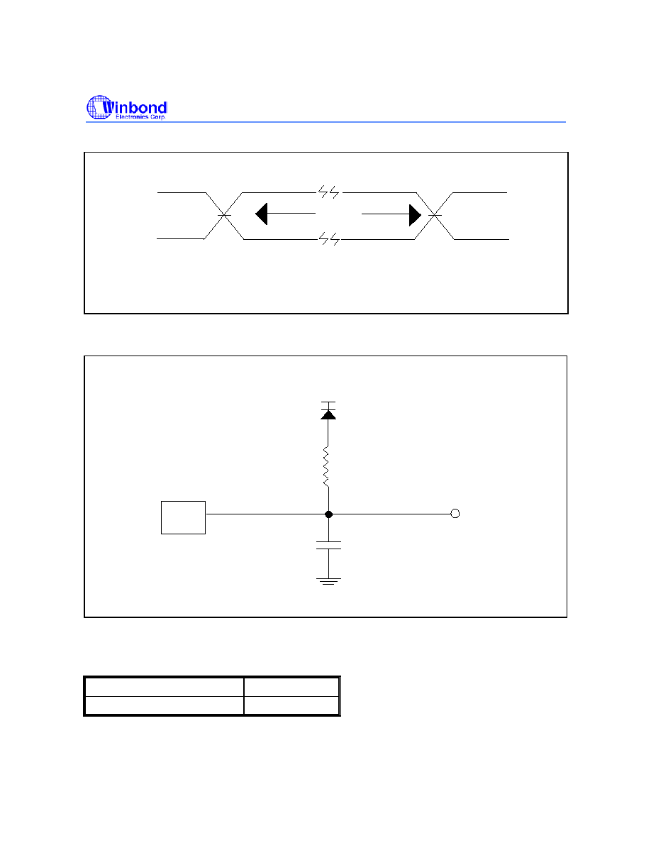
W28J321B/T
- 34 -
AC Input/Output Test Conditions
2.7
0.0
INPUT
1.35
1.35 OUTPUT
TEST POINTS
AC test inputs are driven at 2.7V for a Logic "1" and 0.0V for a Logic "0". Input timing begins,
and output timing ends, at 1.35V. Input rise and fall times (10% to 90%) <10 nS.
Figure 14. Transient Input/Output Reference Waveform for V
DD
= 2.7V to 3.6V
+1.3V
Includes Jig Capacitance
(IN914)
DEVICE
UNDER
TEST
OUT
=3.3K ohm
R
L
C
L
C
L
Figure 15. Transient Equivalent Testing Load Circuit
Test Configuration Capacitance Loading Value
TEST CONFIGURATION
CL(PF)
V
DD
= 2.7V to 3.6V
50
W28J321B/T
Publication Release Date: April 11, 2003
- 35 -
Revision A4
DC Characteristics
V
DD
= 2.7V
- 3.6V
PARAMETER SYM.
TEST
CONDITIONS
Typ. Max.
UNIT
Input Load Current
(note 1)
I
LI
V
DD
= V
DD
Max.
V
IN
= V
DD
or V
SS
�0.5
�A
Output Leakage Current
(note1)
I
LO
V
DD
= V
DD
Max.
V
OUT
= V
DD
or V
SS
�0.5
�A
V
DD
Standby Current
(note 1)
I
CCS
V
DD
= V
DD
Max. #CE =
#RESET = V
DD
�0.2V
4 20
�A
V
DD
Auto Power-Save Current
(note 1, 4)
I
CCAS
V
DD
= V
DD
Max.
#CE = V
SS
�0.2V
4 20
�A
V
DD
Reset Power-Down Current
(note 1)
I
CCD
#RESET = V
SS
�0.2V
4 20
�A
V
DD
Read Current
(note 1)
I
CCR
V
DD
= V
DD
Max.,
#CE = V
SS
, f = 5 MHz,
I
OUT
= 0 mA
15 30
mA
V
PP
= 2.7V
- 3.6V
5 17
mA
V
DD
Word Write or Set Lock-Bit Current
(note 1, 5)
I
CCW
V
PP
= 11.7V
- 12.3V
5 12
mA
V
PP
= 2.7V
- 3.6V
4 17
mA
V
DD
Block Erase, Full Chip Erase or
Clear Block Lock-Bits Current (note 1, 5)
I
CCE
V
PP
= 11.7V
- 12.3V
4 12
mA
V
DD
Word Write or Block Erase Suspend
Current (note 1, 2)
I
CCWS
I
CCES
#CE = V
IH
1
6
mA
I
CCWS
V
PP
V
DD
�2
�15
�A
V
PP
Standby or Read Current
(note 1)
I
CCWR
V
PP
> V
DD
10
200
�A
V
PP
Auto Power-Save Current
(note 1, 4)
I
CCWAS
V
DD
= V
DD
Max.
#CE= V
SS
�0.2V
0.1 5
�A
V
PP
Reset Power-down Current (note 1)
I
CCWD
#RESET = V
SS
�0.2V
0.1 5
�A
V
PP
= 2.7V � 3.6V
12
40
mA
V
PP
Word Write or Set Lock- Bit Current
(note 1, 5)
I
CCWW
V
PP
= 11.7V
- 12.3V
30
mA
V
PP
= 2.7V
- 3.6V
8 25
mA
V
PP
Block Erase, Full Chip Erase or
Clear Block Lock-Bits Current (note 1, 5)
I
CCWE
V
PP
= 11.7V
- 12.3V
20
mA
V
PP
Word Write or Block Erase Suspend
Current (note 1)
I
CCWWS
I
CCWES
V
PP
= V
PPH1/2
10
200
�A
W28J321B/T
- 36 -
DC Characteristics (continued)
V
DD
= 2.7V
- 3.6V
PARAMETER SYM.
TEST
CONDITIONS
Min.
Max.
UNIT
Input Low Voltage (note 5)
V
IL
-0.5
0.4
V
Input High Voltage (note 5)
V
IH
V
DD
-0.4
V
DD
+0.5
V
Output Low Voltage (note 5)
V
OL
V
DD
= V
DD
Min.
I
OL
= 2.0 mA
0.4 V
Output High Voltage (note 5)
V
OH
V
DD
= V
DD
Min.
I
OH
= -2.0 mA
V
DD
-0.4
V
V
PP
Lockout during Normal Operations
(note 3, 5)
V
PPLK
1.0
V
V
PP
during Block Erase, Full Chip Erase, Word
Write or Lock-Bit Configuration Operations
V
PPH1
2.7
3.6
V
V
PP
during Block Erase, Full Chip Erase, Word
Write or Lock-Bit Configuration Operations
(note 6)
V
PPH2
11.7
12.3
V
V
DD
Lockout Voltage
V
LKO
2.0
V
Notes:
1. All currents are in RMS unless otherwise noted. Typical values at nominal V
DD
voltage and T
A
= +25
� C.
2. I
CCWS
and I
CCES
are specified with the device de-selected. If read or word written while in erase suspend mode, the device's
current draw is the sum of I
CCWS
or I
CCES
and I
CCR
or I
CCW
, respectively.
3. Block erases, full chip erase, word writes and lock-bit configurations are inhibited when V
PP
V
PPLK
, and not guaranteed in the
range between V
PPLK
(max.) and V
PPH1
(min.), between V
PPH1
(max.) and V
PPH2
(min.) and above V
PPH2
(max.).
4. The Automatic Power Savings (APS) feature is placed automatically power save mode that addresses not switching more
than 300 nS while read mode.
5. Sampled, not 100% tested.
6. Applying 12V
�0.3V to V
PP
during erase/write can only be done for a maximum of 1000 cycles on each block. V
PP
may be
connected to 12V
�0.3V for a total of 80 hours maximum.

W28J321B/T
Publication Release Date: April 11, 2003
- 37 -
Revision A4
AC Characteristics - Read-only Operations(1)
V
DD
= 2.7V to 3.6V, TA = -40
�C to +85�C
PARAMETER SYM.
MIN.
MAX.
UNIT
Read Cycle Time
t
AVAV
90
nS
Address to Output Delay
t
AVQV
90 nS
#CE to Output Delay (note 2)
t
ELQV
90 nS
#RESET High to Output Delay
t
PHQV
600
nS
#OE to Output Delay (note 2)
t
GLQV
40 nS
#CE to Output in Low Z (note 3)
t
ELQX
0
nS
#CE High to Output in High Z (note 3)
t
EHQZ
40 nS
#OE to Output in Low Z (note 3)
t
GLQX
0
nS
#OE High to Output in High Z (note 3)
t
GHQZ
15 nS
Output Hold from Address, #CE or #OE Change,
Whichever Occurs First (note 3)
t
OH
0 nS
Notes:
1. See AC Input/Output Reference Waveform for maximum allowable input slew rate.
2. #OE may be delayed up to t
ELQV
to t
GLQV
after the falling edge of #CE without impact on t
ELQV
.
3. Sampled, not 100% tested.
VIH
VIL
Address(A)
#OE(G)
#WE(W)
#CE(E)
t
GHQZ
VIH
VIL
Standby
Device
Address Selection
Data Valid
Address Stable
VIH
VIL
VIH
VIL
t
EHQZ
VIH
VIL
DATA(D/Q)
(DQ0-DQ15)
VOH
VOL
V
DD
#RESET(P)
HIGH Z
HIGH Z
t
GLQV
t
ELQV
t
ELQX
t
GLQX
t
OH
Valid Output
t
AVAV
t
AVQV
t
PHQV
Figure 16. AC Waveform for Read Operations
W28J321B/T
- 38 -
AC Characteristics - Write Operations(1)
V
DD
= 2.7V to 3.6V, TA = -40
�C to +85�C
PARAMETER SYM.
MIN.
MAX.
UNIT
Write Cycle Time
t
AVAV
90 nS
#RESET High Recovery to #WE Going Low (note 2)
t
PHWL
1
�S
#CE Setup to #WE Going Low
t
ELWL
10 nS
#WE Pulse Width
t
WLWH
50 nS
#WP V
IH
Setup to #WE Going High (note 2)
t
SHWH
100 nS
V
PP
Setup to #WE Going High (note 2)
t
VPWH
100 nS
Address Setup to #WE Going High (note 3)
t
AVWH
50 nS
Data Setup to #WE Going High (note 3)
t
DVWH
50 nS
Data Hold from #WE High
t
WHDX
0 nS
Address Hold from #WE High
t
WHAX
0 nS
#CE Hold from #WE High
t
WHEH
10 nS
#WE Pulse Width High
t
WHWL
30 nS
#WE High to SR.7 Going "0"
t
WHR0
100
nS
Write Recovery before Read
t
WHGL
0 nS
V
PP
Hold from Valid SRD (note 2, 4)
t
QVVL
0 nS
#WP V
IH
Hold from Valid SRD (note 2, 4)
t
QVSL
0 nS
Notes:
1. Read timing characteristics during block erase, full chip erase, word write and lock-bit configuration operations are the same
as during read-only operations. Refer to AC Characteristics for read-only operations.
2. Sampled, not 100% tested.
3. Refer to Table 3 for valid AIN and DIN for block erase, full chip erase, word write or lock-bit configuration.
4. V
PP
should be held at V
PPH1/2
until determination of block erase, full chip erase, word write or lock-bit configuration success
(SR.1/3/4/5 = 0).

W28J321B/T
Publication Release Date: April 11, 2003
- 39 -
Revision A4
Address(A)
#OE(G)
#WE(W)
#CE(E)
VIH
VIL
VIH
VIL
VIH
VIL
t
WLWH
t
WHQV1,2,3,4
DATA(D/Q)
VIH
HIGH Z
t
WHGL
VIH
VIL
AIN
AIN
t
AVAV
ELWL
t
WHEH
t
t
AVWH
t
WHAX
t
WHWL
t
DVWH
t
WHDX
D
IN
D
IN
Valid
SRD
D
IN
t
PHWL
VIL
RY/#BY(R)
High Z
("1")
VOL
("0")
t
WHR0
#WP(S)
IH
IL
V
V
t
SHWH
t
QVSL
t
#RESET(P)
IH
IL
V
V
VPWH
t
PPH1/2
V
PPLK
V
IL
V
QVVL
t
(V)
VPP
1
2
3
4
5
6
Figure 17. AC Waveform for #WE-Controlled Write Operations
Notes:
1. V
DD
power-up and standby.
2. Write each setup command.
3. Write each confirm command or valid address and data.
4. Automated erase or program delay.
5. Read status register data.
6. Write Read Array command.
W28J321B/T
- 40 -
Alternative #CE - Controlled Writes(1)
V
DD
= 2.7V to 3.6V, TA = -40
�C to +85�C
PARAMETER SYM.
MIN.
MAX.
UNIT
Write Cycle Time
t
AVAV
90 nS
#RESET High Recovery to #CE Going Low (note 2)
t
PHEL
1 nS
#WE Setup to #CE Going Low
t
WLEL
0 nS
#CE Pulse Width
t
ELEH
65 nS
#WP V
IH
Setup to #CE Going High (note 2)
t
SHEH
100 nS
V
PP
Setup to #CE Going High (note 2)
t
VPEH
100 nS
Address Setup to #CE Going High (note 3)
t
AVEH
50 nS
Data Setup to #CE Going High (note 3)
t
DVEH
50 nS
Data Hold from #CE High
t
EHDX
0 nS
Address Hold from #CE High
t
EHAX
0 nS
#WE Hold from #CE High
t
EHWH
0 nS
#CE Pulse Width High
t
EHEL
25 nS
#CE High to SR.7 Going "0"
t
EHR0
100
nS
Write Recovery before Read
t
EHGL
0 nS
V
PP
Hold from Valid SRD (note 2, 4)
t
QVVL
0 nS
#WP V
IH
Hold from Valid SRD (note 2, 4)
t
QVSL
0 nS
Notes:
1. In systems where #CE defines the write pulse width (within a longer #WE timing waveform), all setup, hold, and inactive #WE
times should be measured relative to the #CE waveform.
2. Sampled, not 100% tested.
3. Refer to Table 3 for valid AIN and DIN for block erase, full chip erase, word write or lock-bit configuration.
4. V
PP
should be held at V
PPH1/2
until determination of block erase, full chip erase, word write or lock-bit configuration success
(SR.1/3/4/5 = 0).

W28J321B/T
Publication Release Date: April 11, 2003
- 41 -
Revision A4
Address(A)
#OE(G)
#WE(W)
#CE(E)
VIH
VIL
VIH
VIL
VIH
VIL
t
WLEL
DATA(D/Q)
VIH
HIGH Z
t
EHGL
VIH
VIL
A IN
A IN
t
AVAV
ELEH
t
EHEL
t
t
AVEH
t
EHAX
t
EHDX
D
IN
D
IN
Valid
SRD
D
IN
t
PHEL
VIL
RY/#BY(R)
High Z
("1")
VOL
("0")
t
EHR0
#WP(S)
IH
IL
V
V
t
SHEH
t
QVSL
t
#RESET(P)
IH
IL
V
V
(V)
VPEH
t
PPH1/2
V
PPLK
V
IL
V
QVVL
t
VPP
1
2
3
4
5
6
t
EHWH
t
EHQV1,2,3,4
DVEH
t
Figure 18. AC Waveform for #CE-Controlled Write Operations
Notes:
1. V
DD
power-up and standby.
2. Write each setup command.
3. Write each confirm command or valid address and data.
4. Automated erase or program delay.
5. Read status register data.
6. Write Read Array command.
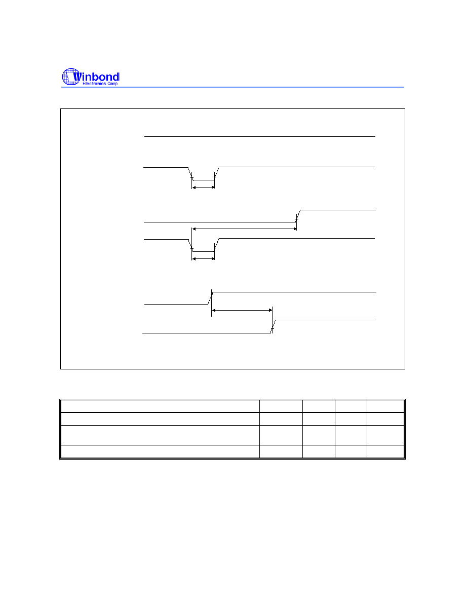
W28J321B/T
- 42 -
Reset Operations
SR.7(R)
("1")
("0")
IH
IL
V
V
#RESET(P)
PLPH
t
(A)Reset During Read Array Mode
(C)#RESET Rising Timing
2.7V
VIL
IH
IL
V
V
#RESET(P)
2VPH
t
SR.7(R)
("1")
("0")
IH
IL
V
V
#RESET(P)
PLPH
t
(B)Reset During Block Erase, Full Chip Erase, Word/Byte Write or Lock-Bit Configuratio
PLR1
t
V
DD
Figure 19. AC Waveform for Reset Operation
Reset AC Specifications
PARAMETER SYM.
MIN.
MAX.
UNIT
#RESET Pulse Low Time (note 2)
t
PLPH
100 nS
#RESET Low to Reset during Block Erase, Full Chip Erase,
Word Write or Lock-Bit Configuration (note 1, 2)
t
PLR1
30
�S
V
DD
2.7V to #RESET High (note 2, 3)
t
2VPH
100 nS
Notes:
1. If #RESET is asserted while a block erase, full chip erase, word write or lock-bit configuration operation is not executing, the
reset will complete within 100ns.
2. A reset time, t
PHQV
, is required from the later of SR.7 going "1" or #RESET going high until outputs are valid. Refer to AC
Characteristics - Read-Only Operations for t
PHQV
.
3. When the device power-up, holding #RESET low minimum 100ns is required after V
DD
has been in predefined range and also
has been in stable there.

W28J321B/T
Publication Release Date: April 11, 2003
- 43 -
Revision A4
Block Erase, Full Chip Erase, Word Write And Lock-Bit Configuration
Performance(3)
V
DD
= 2.7V to 3.6V, TA = -40
�C to +85�C
V
PP
= 2.7V
- 3.6V
V
PP
= 11.7V
- 12.3V
SYM.
PARAMETER NOTE
Min. Typ.(1) Max. Min. Typ.(1) Max.
UNIT
32K word Block
2 33
200 20
�S
t
WHQV1
t
EHQV1
Word Write Time
4K word Block
2 36
200 27
�S
32K
word
Block 2 1.1 4 0.66 S
Block Write Time
(In word mode)
4K
word
Block 2 0.15
0.5 0.12 S
32K word Block
2
1.2
6
0.9
S
t
WHQV2
t
EHQV2
Block Erase Time
4K word Block
2
0.6
5
0.5
S
Full Chip Erase Time
2
84
420
64
S
t
WHQV3
t
EHQV3
Set Lock-Bit Time
2
56
200
42
�S
t
WHQV4
t
EHQV4
Clear Block Lock-Bits Time
2
1
5
0.69
S
t
WHR11
t
EHR11
Word Write Suspend Latency Time
to Read
4 6
15 6 15
�S
t
WHR12
t
EHR12
Block Erase Suspend Latency Time
to Read
4 16 30 16 30
�S
t
ERES
Latency Time from Block Erase
Resume Command to Block Erase
Suspend Command
5 600 600
�S
Notes:
1. Typical values measured at T
A
= +25
� C and V
DD
= 3.0V, V
PP
= 3.0V or 12.0V. Assumes corresponding lock-bits are not set.
Subject to change based on device characterization.
2. Excludes system-level overhead.
3. Sampled but not 100% tested.
4. A latency time is required from issuing suspend command(#WE or #CE going high) until SR.7 going "1".
5. If the time between writing the Block Erase Resume command and writing the Block Erase Suspend command is shorter than
t
ERES
and both commands are written repeatedly, a longer time is required than standard block erase until the completion of
the operation.

W28J321B/T
- 44 -
12. ADDITIONAL INFORMATION
Recommended Operating Conditions
At Device Power-Up
AC timing illustrated in Figure 20 is recommended for the supply voltages and the control signals at
device power-up. If the timing in the figure is ignored, the device may not operate correctly.
VIH
VIL
DD
VIH
VIL
VIH
VIL
#OE
Valid Address
V
DD
V
Vss
(min)
t
VR
t
R
t
2VPH
t
PHQV
*1
#RESET(p)
*2
Vpp (V)
Vss
V
PPH1/2
ADDRESS
VIH
VIL
(A)
t
t
R or F
t
t
R or F
t
AVQV
#CE (E)
t
R
t
F
t
ELQV
t
GLQV
#WE (W)
VIH
VIL
(G)
t
F
t
R
#WP (S)
VIH
VIL
DATA (D/Q)
VOH
VOL
Valid Output
HIGH Z
*1 t
5VPH
for the device in 5V operations.
*2 To prevent the unwanted writes, system designers should consider the V
PP
switch, which connects V
PP
to V
SS
during read
operations and V
PPH1/2
during write or erase operations.
Figure 20. AC Timing at Device Power-up
For the AC specifications t
VR
, t
R
, t
F
in the figure, refer to the next page. See the "ELECTRICAL SPECIFICATIONS" described in
specifications for the supply voltage range, the operating temperature and the AC specifications not shown in the next page.

W28J321B/T
Publication Release Date: April 11, 2003
- 45 -
Revision A4
Rise and Fall Time
PARAMETER SYMBOL
MIN.
MAX.
UNIT
V
DD
Rise Time (note 1)
t
VR
0.5
30000
�S/ V
Input Signal Rise Time (note1, 2)
t
R
1
�S/ V
Input Signal Fall Time (note1, 2)
t
F
1
�S/ V
Notes:
1. Sampled, not 100% tested.
2. This specification is applied for not only the device power-up but also the normal operations. t
R
(Max.) and t
F
(Max.) for
#RESET are 50�s/V
Glitch Noises
Do not input the glitch noises which are below V
IH
(Min.) or above V
IL
(Max.) on address, data, reset,
and control signals, as shown in Figure 21 (b). The acceptable glitch noises are illustrated in Figure 21
(a).
Input Singal
V
IH
(Min.)
Input Singal
V
IH
(Min.)
V
IL
(Max.)
Input Singal
V
IL
(Max.)
Input Singal
(a) Acceptable Glitch Noises
(b) NOT Acceptable Glitch Noises
Figure 21. Waveform for Glitch Noises
See the "DC CHARACTERISTICS" described in specifications for
V
IH
(Min.) and
V
IL
(Max.).

W28J321B/T
- 46 -
13. ORDERING INFORMATION
PART NO.
ACCESS
TIME
(nS)
OPERATING
TEMPERATURE
(
�C)
BOOT BLOCK
PACKAGE
W28J321BB90L 90
-40� C to 85
� C
Bottom Boot
48-Ball
TFBGA
W28J321BT90L
90
-40� C to 85� C
Top Boot
48-Ball
TFBGA
Notes:
1. Winbond reserves the right to make changes to its products without prior notice.
2. Purchasers are responsible for performing appropriate quality assurance testing on products intended for use in applications
where personal injury might occur as a consequence of product failure.
14. PACKAGE DIMENSION
48-Ball TFBGA (measurements in millimeters)
SYMBOL
A
A1
D
D2
E
E2
y
b
e
MILLIMETER
-
-
1.05
MIN. NOM. MAX.
0.20 0.25 0.30
7.80 8.00
8.20
5.25 BASIC
10.80 11.00 11.20
3.75 BASIC
0.10 BASIC
0.37 0.40 0.43
0.75 BASIC
INCH
-
-
0.042
MIN. NOM. MAX.
0.008 0.010 0.012
0.312 0.320 0.328
0.210
0.150 BASIC
0.004 BASIC
0.015 0.016 0.017
0.030 BASIC
0.432 0.440 0.448
CONTROL DIMENSIONS ARE IN MILLIMETERS
A
B
C
D
E
F
G
H

W28J321B/T
Publication Release Date: April 11, 2003
- 47 -
Revision A4
15. VERSION HISTORY
VERSION DATE PAGE
DESCRIPTION
A1
May 27, 2002
-
Initial Issued
A2
Aug. 6, 2002
All
Update description and correct typo
A3
Nov. 18, 2002
44
Correct the typo in Figure 20
A4
Apr. 11, 2003
All
Update description and correct typo
Headquarters
No. 4, Creation Rd. III,
Science-Based Industrial Park,
Hsinchu, Taiwan
TEL: 886-3-5770066
FAX: 886-3-5665577
http://www.winbond.com.tw/
Taipei Office
TEL: 886-2-8177-7168
FAX: 886-2-8751-3579
Winbond Electronics Corporation America
2727 North First Street, San Jose,
CA 95134, U.S.A.
TEL: 1-408-9436666
FAX: 1-408-5441798
Winbond Electronics (H.K.) Ltd.
No. 378 Kwun Tong Rd.,
Kowloon, Hong Kong
FAX: 852-27552064
Unit 9-15, 22F, Millennium City,
TEL: 852-27513100
Please note that all data and specifications are subject to change without notice.
All the trade marks of products and companies mentioned in this data sheet belong to their respective owners.
Winbond Electronics (Shanghai) Ltd.
200336 China
FAX: 86-21-62365998
27F, 2299 Yan An W. Rd. Shanghai,
TEL: 86-21-62365999
Winbond Electronics Corporation Japan
Shinyokohama Kohoku-ku,
Yokohama, 222-0033
FAX: 81-45-4781800
7F Daini-ueno BLDG, 3-7-18
TEL: 81-45-4781881
9F, No.480, Rueiguang Rd.,
Neihu District, Taipei, 114,
Taiwan, R.O.C.