
W28V400B/T
4M(512K
� 8/256K � 16)
SMARTVOLTAGE FLASH MEMORY
Publication Release Date: April 11, 2003
- 1 -
Revision A4
Table of Contents-
1. GENERAL DESCRIPTION.................................................................................................................. 3
2. FEATURES ......................................................................................................................................... 3
3. PRODUCT OVERVIEW ...................................................................................................................... 4
4. BLOCK DIAGRAM .............................................................................................................................. 5
5. PIN CONFIGURATION ....................................................................................................................... 6
6. PIN DESCRIPTION............................................................................................................................. 7
7. PRINCIPLES OF OPERATION........................................................................................................... 8
Data Protection ................................................................................................................................ 8
8. BUS OPERATION............................................................................................................................. 10
Read............................................................................................................................................... 10
Output Disable ............................................................................................................................... 10
Standby .......................................................................................................................................... 10
Deep Power-down.......................................................................................................................... 10
Read Identifier Codes Operation ................................................................................................... 11
Write ............................................................................................................................................... 11
9. COMMAND DEFINITIONS................................................................................................................ 11
Read Array Command ................................................................................................................... 13
Read Identifier Codes Command................................................................................................... 13
Read Status Register Command ................................................................................................... 14
Clear Status Register Command ................................................................................................... 14
Block Erase Command .................................................................................................................. 14
Word/Byte Write Command ........................................................................................................... 15
Block Erase Suspend Command ................................................................................................... 15
Word/Byte Write Suspend Command ............................................................................................ 16
Considerations of Suspend............................................................................................................ 16
Block Locking ................................................................................................................................. 16
10. DESIGN CONSIDERATIONS ......................................................................................................... 22
Three-line Output Control............................................................................................................... 22
RY/#BY, Block Erase and Word/Byte Write Polling....................................................................... 22
Power Supply Decoupling .............................................................................................................. 22

W28V400B/T
- 2 -
V
PP
Trace on Printed Circuit Boards .............................................................................................. 22
V
DD
, V
PP
, #RESET Transitions ...................................................................................................... 22
Power-up/Down Protection ............................................................................................................ 23
Power Dissipation .......................................................................................................................... 23
11. ELECTRICAL SPECIFICATIONS ................................................................................................... 24
Absolute Maximum Ratings* .......................................................................................................... 24
Operating Conditions ..................................................................................................................... 24
Capacitance(1)............................................................................................................................... 24
AC Input/Output Test Conditions ................................................................................................... 25
DC Characteristics ......................................................................................................................... 27
AC Characteristics - Read-only Operations(1) .............................................................................. 29
AC Characteristics - Write Operations(1) ...................................................................................... 33
Alternative #CE-Controlled Writes(1)............................................................................................. 37
Reset Operations ........................................................................................................................... 41
Block Erase And Word/Byte Write Performance(3) ....................................................................... 42
12. FLASH MEMORY W28V400 FAMILY DATA PROTECTION ......................................................... 44
Recommended Operating Conditions............................................................................................ 45
13. ORDERING INFORMATION........................................................................................................... 47
14. PACKAGE DIMENSION.................................................................................................................. 47
48-Lead Standard Thin Small Outline Package (measured in millimeters)................................... 47
15. VERSION HISTORY ....................................................................................................................... 48

W28V400B/T
1. GENERAL DESCRIPTION
The W28V400B/T Flash memory with SmartVoltage technology is a high-density, cost-effective,
nonvolatile, read/write storage solution for a wide range of applications. It operates off of V
DD
= 2.7V
and V
PP
= 2.7V. This low voltage operation capability realize battery life and suits for cellular phone
application. Its Boot, Parameter and Main-blocked architecture, as well as low voltage and extended
cycling. These features provide a highly flexible device suitable for portable terminals and personal
computers. Additionally, the enhanced suspend capabilities provide an ideal solution for both code
and data storage applications. For secure code storage applications, such as networking where code
is either directly executed out of flash or downloaded to DRAM, the device offers four levels of
protection. These are: absolute protection, enabled when V
PP
V
PPLK
; selective hardware blocking;
flexible software blocking; or write protection. These alternatives give designers comprehensive
control over their code security needs. The device is manufactured on 0.35
�m process technology. It
comes in industry-standard package: the 48-lead TSOP, ideal for board constrained applications.
2. FEATURES
�
SmartVoltage Technology
- V
DD
= 2.7V, 3.3V or 5V
- V
PP
= 2.7V, 3.3V, 5V or 12V
�
User-Configurable x 8 or x 16 Operation
�
High-Performance Access Time
- 85 nS (5V �0.25V), 90 nS (5V �0.5V),
100 nS (3.3V
�0.3V), 120 nS (2.7V to 3.6V)
�
Operating Temperature
- 0� C to +70� C
�
Optimized Array Blocking Architecture
- Two 4k-word (8k-byte) Boot Blocks
- Six 4k-word (8k-byte) Parameter Blocks
- Seven 32k-word (64k-byte) Main Blocks
- Top Boot Location (W28V400TT)
- Bottom Boot Location (W28V400BT)
�
Extended Cycling Capability
- Minimum 100,000 Block Erase Cycles
�
Low Power Management
- Deep Power-down Mode
- Automatic Power Savings Mode Decreases
I
CCR
in Static Mode
�
Enhanced Automated Suspend Options
- Word/Byte Write Suspend to Read
- Block Erase Suspend to Word/Byte Write
- Block Erase Suspend to Read
�
Enhanced Data Protection Features
- Absolute Protection with V
PP
V
PPLK
- Block Erase, Full Chip Erase, Word/Byte
Write and Lock-Bit Configuration Lockout
during Power Transitions
- Block Blocks Protection with #WP = V
IL
�
Automated Word/Byte Write and Block Erase
- Command User Interface (CUI)
- Status Register (SR)
�
SRAM-Compatible Write Interface
�
Industry-Standard Packaging
- 48-Lead TSOP
Publication Release Date: April 11, 2003
- 3 -
Revision A4

W28V400B/T
- 4 -
3. PRODUCT OVERVIEW
The W28V400B/T is a high-performance 4M-bit SmartVoltage Flash memory organized as 512k-byte
of 8 bits or 256k-word of 16 bits. The 512k-byte/256k-word of data is arranged in two 8k-byte/4k-word
boot blocks, six 8k-byte/4k-word parameter blocks and seven 64kbyte/32k-word main blocks which
are individually erasable in-system. The memory map is shown in Figure 3.
SmartVoltage technology provides a choice of V
DD
and V
PP
combinations, as shown in Table 1, to
meet system performance and power expectations. 2.7V V
DD
consumes approximately one-fifth the
power of 5V V
DD
. But, 5V V
DD
provides the highest read performance. V
PP
at 2.7, 3.3V and 5V
eliminates the need for a separate 12V converter, while V
PP
= 12V maximizes block erase and
word/byte write performance. In addition to flexible erase and program voltages, the dedicated V
PP
pin
gives complete data protection when V
PP
V
PPLK
.
Table 1. V
DD
and
V
PP
Voltage Combinations Offered by SmartVoltage Technology
V
DD
VOLTAGE
V
PP
VOLTAGE
2.7V
2.7V, 3.3V, 5V, 12V
3.3V
3.3V, 5V, 12V
5V 5V,
12V
Internal V
DD
and V
PP
detection Circuitry automatically configures the device for optimized read and
write operations.
A Command User Interface (CUI) serves as the interface between the system processor and internal
operation of the device. A valid command sequence written to the CUI initiates device automation. An
internal Write State Machine (WSM) automatically executes the algorithms and timings necessary for
block erase and word/byte write operations.
A block erase operation erases one of the device's 32k-word blocks typically within 0.39s (5V V
DD
,
12V V
PP
), 4k-word blocks typically within 0.25s (5V V
DD
, 12V V
PP
) independent of other blocks. Each
block can be independently erased 100,000 times. Block erase suspend mode allows system software
to suspend block erase to read or write data from any other block.
Writing memory data is performed in word/byte increments of the device's 32k-word blocks typically
within 8.4
�S (5V V
DD
, 12V V
PP
), 4k-word blocks typically within 17
�S (5V V
DD
, 12V V
PP
). Word/byte
write suspend mode enables the system to read data or execute code from any other flash memory
array location.
The boot blocks can be locked for the #WP pin. Block erase or word/byte write for boot block must not
be carried out by #WP to Low and #RESET to V
IH
.
The status register indicates when the WSM's block erase or word/byte write operation is finished.
The RY/#BY output gives an additional indicator of WSM activity by providing both a hardware signal
of status (versus software polling) and status masking (interrupt masking for background block erase,
for example). Status polling using RY/#BY minimizes both CPU overhead and system power
consumption. When low, RY/#BY indicates that the WSM is performing a block erase or word/byte
write. RY/#BY-high indicates that the WSM is ready for a new command, block erase is suspended
(and word/byte write is inactive), word/byte write is suspended, or the device is in deep power-down
mode.
W28V400B/T
Publication Release Date: April 11, 2003
- 5 -
Revision A4
The access time is 85ns (t
AVQV
) over the commercial temperature range (0
� C to +70� C) and V
DD
supply voltage range of 4.75V to 5.25V. At lower V
DD
voltages, the access times are 90ns (4.5V to
5.5V), 100 nS (3.0V to 3.6V) and 120 nS (2.7V to 3.6V).
The Automatic Power Savings (APS) feature substantially reduces active current when the device is in
static mode (addresses not switching). In APS mode, the typical I
CCR
current is 1mA at V
DD
= 5V
.
When #CE and #RESET pins are at V
DD
, the I
CC
CMOS standby mode is enabled. When the #RESET
pin is at V
SS
, deep power-down mode is enabled which minimizes power consumption and provides
write protection during reset. A reset time (tPHQV) is required from #RESET switching high until
outputs are valid. Likewise, the device has a wake time (tPHEL) from #RESET-high until writes to the
CUI are recognized. With #RESET at V
SS
, the WSM is reset and the status register is cleared.
The device is available in 48-lead TSOP (Thin Small Outline Package, 1.2 mm thick). Pinout is shown
in Figure 2.
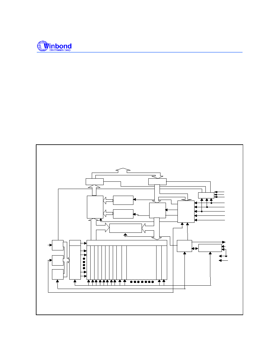
4. BLOCK DIAGRAM
Y-Gating
32K-Word
(64K-Byte)
Main Blocks
x 7
Output Buffer
DQ0 -DQ15
Input Buffer
Identifier
Register
Output
Multiplexer
Status
Register
Data
Register
Command
User
Interface
I/O Logic
Data
Comparator
A-1
Input
Buffer
Address
Latch
Address
Counter
Y
Decoder
X
Decoder
Write
State
Machine
Program/Erase
Voltage Switch
VDD
#BYTE
#CE
#WE
#OE
#RESET
#WP
RY/#BY
VPP
VDD
VSS
A0-A17
P
a
ra
m
e
te
r B
l
o
ck 0
P
a
ra
m
e
te
r B
l
o
ck 1
P
a
ra
m
e
te
r B
l
o
ck 2
P
a
ra
m
e
te
r B
l
o
ck 3
P
a
ra
m
e
te
r B
l
o
ck 4
P
a
ra
m
e
te
r B
l
o
ck 5
Boot Bloc
k
0
Boot Bloc
k
1
M
a
i
n
B
l
o
ck 0
M
a
i
n
B
l
o
ck 1
M
a
i
n
B
l
o
ck 5
M
a
i
n
B
l
o
ck 6
Figure 1. Block Diagram