
W39L512
64K
◊
8 CMOS FLASH MEMORY
Publication Release Date: July 9, 2002
- 1 - Revision A2
1. GENERAL DESCRIPTION
The W39L512 is a 512Kbit, 3.3-volt only CMOS flash memory organized as 64K
◊
8 bits. For flexible
erase capability, the 512Kbits of data are divided into 16 small even pages with 4 Kbytes. The byte-
wide (
◊
8) data appears on DQ7
-
DQ0. The device can be programmed and erased in-system with a
standard 3.3V power supply. A 12-volt V
PP
is not required. The unique cell architecture of the
W39L512 results in fast program/erase operations with extremely low current consumption (compared
to other comparable 3.3-volt flash memory products). The device can also be programmed and erased
by using standard EPROM programmers.
2. FEATURES
∑
Single 3.3-volt operations
-
3.3-volt Read
-
3.3-volt Erase
-
3.3-volt Program
∑
Fast Program operation:
-
Byte-by-Byte programming: 50
µ
S (max.)
∑
Fast Erase operation: 100 mS (max.)
∑
Read access time: 70/90 nS
∑
16 even pages with 4K bytes
∑
Any individual page can be erased
∑
Hardware protection:
-
Optional 8K byte Top/Bottom Boot Block with
lockout protection
∑
Flexible 4K-page size can be used as
Parameter Blocks
∑
Typical program/erase cycles:
-
1K/10K
∑
Twenty-year data retention
∑
Low power consumption
-
Active current: 10 mA (typ.)
-
Standby current: 15
µ
A (typ.)
∑
End of program detection
-
Software method: Toggle bit/Data polling
∑
TTL compatible I/O
∑
JEDEC standard byte-wide pinouts
∑
Available packages: 32-pin PLCC and
32-pin STSOP (8 x 14 mm)
W39L512
- 2 -
3. PIN CONFIGURATIONS
5
6
7
9
10
11
12
13
A7
A6
A5
A4
A3
A2
A1
A0
DQ0
29
28
27
26
25
24
23
22
21
30
31
32
1
2
3
4
8
20
19
18
17
16
15
14
D
Q
1
D
Q
2
D
Q
3
D
Q
4
D
Q
5
D
Q
6
A14
A13
A8
A9
A11
#OE
A10
#CE
DQ7
A
1
2
V
D
D
#
W
E
A
1
5
32-pin
PLCC
N
C
V
S
S
N
C
N
C
1
2
3
4
5
6
7
8
9
10
11
12
13
14
15
16
A3
A2
A1
A0
DQ0
DQ1
DQ2
V
#OE
A10
#CE
DQ7
DQ6
DQ5
DQ4
DQ3
32-pin
STSOP
A15
A12
A7
A6
A5
A4
V
#WE
A14
A13
A8
DD
A11
A9
NC
32
31
30
29
28
27
26
25
24
23
22
21
20
19
18
17
SS
NC
NC
4. BLOCK DIAGRAM
CONTROL
OUTPUT
BUFFER
DECODER
CORE
ARRAY
#CE
#OE
#WE
A0
.
.
A15
.
.
DQ0
DQ7
V
DD
V
SS
5. PIN DESCRIPTION
SYMBOL
PIN NAME
A0
-
A15
Address Inputs
DQ0
-
DQ7
Data Inputs/Outputs
#CE
Chip Enable
#OE
Output Enable
#WE
Write Enable
V
DD
Power Supply
V
SS
Ground
NC
No Connections

W39L512
Publication Release Date: July 9, 2002
- 3 - Revision A2
6. FUNCTIONAL DESCRIPTION
Device Bus Operation
Read Mode
The read operation of the W39L512 is controlled by #CE and #OE, both of which have to be low for the
host to obtain data from the outputs. #CE is used for device selection. When #CE is high, the chip is
de-selected and only standby power will be consumed. #OE is the output control and is used to gate
data from the output pins. The data bus is in high impedance state when either #CE or #OE is high.
Refer to the timing waveforms for further details.
Write Mode
Device erasure and programming are accomplished via the command register. The contents of the
register serve as inputs to the internal state machine. The state machine outputs dictate the function of
the device.
The command register itself does not occupy any addressable memory location. The register is a latch
used to store the commands, along with the address and data information needed to execute the
command. The command register is written to bring #WE to logic low state, while #CE is at logic low
state and #OE is at logic high state. Addresses are latched on the falling edge of #WE or #CE,
whichever happens later; while data is latched on the rising edge of #WE or #CE, whichever happens
first. Standard microprocessor write timings are used.
Refer to AC Write Characteristics and the Erase/Programming Waveforms for specific timing
parameters.
Standby Mode
There are two ways to implement the standby mode on the W39L512 device, both using the #CE pin.
A CMOS standby mode is achieved with the
#CE
input held at
V
DD
±
0.3V. Under this condition the current
is typically reduced to less than 20
µ
A. A TTL standby mode is achieved with the #CE pin held at V
IH
.
Under this condition the current is typically reduced to 2 mA.
In the standby mode the outputs are in the high impedance state, independent of the #OE input.
Output Disable Mode
With the #OE input at a logic high level (V
IH
), output from the device is disabled. This will cause the
output pins to be in a high impedance state.
Auto-select Mode
The auto-select mode allows the reading of a binary code from the device and will identify its
manufacturer and type. This mode is intended for use by programming equipment for the purpose of
automatically matching the device to be programmed with its corresponding programming algorithm.
This mode is functional over the entire temperature range of the device.
To activate this mode, the programming equipment must force V
ID
(11.5V to 12.5V) on address pin A9.
Two identifier bytes may then be sequenced from the device outputs by toggling address A0 from V
IL
to V
IH
. All addresses are don
t cares except A0 and A1 (see "Auto-select Codes").

W39L512
- 4 -
The manufacturer and device codes may also be read via the command register, for instance, when
the W39L512
is erased or programmed in a system without access to high voltage on the A9 pin. The
command sequence is illustrated in "Auto-select Codes".
Byte 0 (A0 = V
IL
) represents the manufacturer
s code (Winbond = DAH) and byte 1 (A0 = V
IH
) the
device identifier code (W39L512 = 38H). All identifiers for manufacturer and device will exhibit odd
parity with DQ7 defined as the parity bit. In order to read the proper device codes when executing the
Auto-select, A1 must be low state.
Data Protection
The W39L512
is designed to offer protection against accidental erasure or programming caused by
spurious system level signals that may exist during power transitions. During power up the device
automatically resets the internal state machine in the Read mode. Also, with its control register
architecture, alteration of the memory contents only occurs after successful completion of specific
multi-bus cycle command sequences. The device also incorporates several features to prevent
inadvertent write cycles resulting from V
DD
power-up and power-down transitions or system noise.
Boot Block Operation
There are two alternatives to set the boot block. The 8K-byte in the top/bottom location of this device
can be locked as boot block, which can be used to store boot codes. It is located in the last 8K bytes or
first 8K bytes of the memory with the address range from E000(hex) to FFFF(hex) for top location or
0000(hex) to 1FFF(hex) for bottom location.
See Command Codes for Boot Block Lockout Enable for the specific code. Once this feature is set the
data for the designated block cannot be erased or programmed (programming lockout), other memory
locations can be changed by the regular programming method.
In order to detect whether the boot block feature is set on the first/last 8K-byte block or not, users can
perform software command sequence: enter the product identification mode (see Command Codes for
Identification/Boot Block Lockout Detection for specific code), and then read from address 0002(hex)
for first(bottom) location or FFF2(hex) for last(top) location. If the DQ0/DQ1 of output data is "1,"
the 8Kbytes boot block programming lockout feature will be activated; if the DQ0/DQ1 of output data is
"0," the lockout feature will be inactivated and the block can be erased/programmed.
To return to normal operation, perform a three-byte command sequence (or an alternate single-byte
command) to exit the identification mode. For the specific code, see Command Codes for
Identification/Boot Block Lockout Detection.
Low
V
DD
Inhibit
To avoid initiation of a write cycle during V
DD
power-up and power-down, the W39L512 locks out when
V
DD
< 2.0V (see DC Characteristics section for voltages). The write and read operations are inhibited
when V
DD
is less than 2.0V typical. The W39L512 ignores all write and read operations until V
DD
>
2,0V. The user must ensure that the control pins are in the correct logic state when V
DD
> 2.0V to
prevent unintentional writes.
Write Pulse "Glitch" Protection
Noise pulses of less than 10 nS (typical) on #OE, #CE, or #WE will not initiate a write cycle.

W39L512
Publication Release Date: July 9, 2002
- 5 - Revision A2
Logical Inhibit
Writing is inhibited by holding any one of #OE = V
IL
, #CE = V
IH
, or #WE = V
IH
. To initiate a write cycle
#CE and #WE must be a logical zero while #OE is a logical one.
Power-up Write Inhibit
Power-up of the device with #WE = #CE = VIL and #OE = V
IH
will not accept commands on the rising
edge of #WE except 5mS delay (see the power up timing in AC Characteristics). The internal state
machine is automatically reset to the read mode on power-up.
Command Definitions
Device operations are selected by writing specific address and data sequences into the command
register. Writing incorrect address and data values or writing them in the improper sequence will reset
the device to the read mode. "Command Definitions" defines the valid register command sequences.
Read Command
The device will automatically power-up in the read state. In this case, a command sequence is not
required to read data. Standard microprocessor read cycles will retrieve array data. This default value
ensures that no spurious alteration of the memory content occurs during the power transition.
The device will automatically returns to read state after completing an Embedded Program or
Embedded Erase algorithm.
Refer to the AC Read Characteristics and Waveforms for the specific timing parameters.
Auto-select Command
Flash memories are intended for use in applications where the local CPU can alter memory contents.
As such, manufacture and device codes must be accessible while the device resides in the target
system. PROM programmers typically access the signature codes by raising A9 to a high voltage.
However, multiplexing high voltage onto the address lines is not generally a desirable system design
practice.
The device contains an auto-select command operation to supplement traditional PROM programming
methodology. The operation is initiated by writing the auto-select command sequence into the
command register. Following the command write, a read cycle from address XX00H retrieves the
manufacture code of DAH. A read cycle from address XX01H returns the device code (W39L512 =
38H).
To terminate the operation, it is necessary to write the auto-select exit command sequence into the
register.
Byte Program Command
The device is programmed on a byte-by-byte basis. Programming is a four-bus-cycle operation. The
program command sequence is initiated by writing two "unlock" write cycles, followed by the program
set-up command. The program address and data are written next, which in turn initiate the Embedded
program algorithm. Addresses are latched on the falling edge of #CE or #WE, whichever happens later
and the data is latched on the rising edge of #CE or #WE, whichever happens first. The rising edge of
#CE or #WE (whichever happens first) begins programming using the Embedded Program Algorithm.

W39L512
- 6 -
Upon executing the algorithm, the system is not required to provide further controls or timings. The
device will automatically provide adequate internally generated program pulses and verify the
programmed cell margin.
The automatic programming operation is completed when the data on DQ7 (also used as Data Polling)
is equivalent to the data written to this bit at which time the device returns to the read mode and
addresses are no longer latched (see "Hardware Sequence Flags"). Therefore, the device requires that
a valid address to the device be supplied by the system at this particular instance of time for Data
Polling operations. Data Polling must be performed at the memory location which is being
programmed.
Any commands written to the chip during the Embedded Program Algorithm will be ignored. If a
hardware reset occurs during the programming operation, the data at that particular location will be
corrupted.
Programming is allowed in any sequence and across page boundaries. Beware that a data "0" cannot
be programmed back to a "1". Attempting to program 0 back to 1, the toggle bit will stop toggling. Only
erase operations can convert "0"s to "1"s.
Refer to the Programming Command Flow Chart using typical command strings and bus operations.
Chip Erase Command
Chip erase is a six-bus-cycle operation. There are two "unlock" write cycles, followed by writing the
"set-up" command. Two more "unlock" write cycles are asserted, followed by the chip erase command.
Chip erase does not require the user to program the device prior to erase. Upon executing the
Embedded Erase Algorithm command sequence the device will automatically erase and verify the
entire memory for an all one data pattern. The erase is performed sequentially on each pages at the
same time (see "Feature"). The system is not required to provide any controls or timings during these
operations.
The automatic erase begins on the rising edge of the last #WE pulse in the command sequence and
terminates when the data on DQ7 is "1" at which time the device returns to read the mode.
Refer to the Erase Command Flow Chart using typical command strings and bus operations.
Page Erase Command
Page erase is a six bus cycles operation. There are two "unlock" write cycles, followed by writing the
"set-up" command. Two more "unlock" write cycles then follows by the page erase command. The
page address (any address location within the desired page) is latched on the falling edge of #WE,
while the command (50H) is latched on the rising edge of #WE.
Page erase does not require the user to program the device prior to erase. When erasing a page, the
remaining unselected pages are not affected. The system is not required to provide any controls or
timings during these operations.
The automatic page erase begins after the erase command is completed, right from the rising edge of
the #WE pulse for the last page erase command pulse and terminates when the data on DQ7, Data
Polling, is "1" at which time the device returns to the read mode. Data Polling must be performed at an
address within any of the pages being erased.
Refer to the Erase Command flow Chart using typical command strings and bus operations.

W39L512
Publication Release Date: July 9, 2002
- 7 - Revision A2
Write Operation Status
DQ7: Data Polling
The W39L512 device features Data Polling as a method to indicate to the host that the embedded
algorithms are in progress or completed.
During the Embedded Program Algorithm, an attempt to read the device will produce the complement
of the data last written to DQ7. Upon completion of the Embedded Program Algorithm, an attempt to
read the device will produce the true data last written to DQ7.
During the Embedded Erase Algorithm, an attempt to read the device will produce a "0" at the DQ7
output. Upon completion of the Embedded Erase Algorithm, an attempt to read the device will produce
a "1" at the DQ7 output.
For chip erase, the Data Polling is valid after the rising edge of the sixth pulse in the six #WE write
pulse sequences. For page erase, the Data Polling is valid after the last rising edge of the page erase
#WE pulse. Data Polling must be performed at addresses within any of the pages being erased.
Otherwise, the status may not be valid.
Just prior to the completion of Embedded Algorithm operations DQ7 may change asynchronously while
the output enable (#OE) is asserted low. This means that the device is driving status information on
DQ7 at one instant of time and then that byte
s valid data at the next instant of time. Depending on
when the system samples the DQ7 output, it may read the status or valid data. Even if the device has
completed the Embedded Algorithm operations and DQ7 has a valid data, the data outputs on DQ0 ≠
DQ6 may be still invalid. The valid data on DQ0
-
DQ7 will be read on the successive read attempts.
The Data Polling feature is only active during the Embedded Programming Algorithm, Embedded
Erase Algorithm, or page erase time-out (see "Command Definitions").
DQ6: Toggle Bit
The W39L512 also features the "Toggle Bit" as a method to indicate to the host system that the
embedded algorithms are in progress or completed.
During an Embedded Program or Erase Algorithm cycle, successive attempts to read (#OE toggling)
data from the device at any address will result in DQ6 toggling between one and zero. Once the
Embedded Program or Erase Algorithm cycle is completed, DQ6 will stop toggling and valid data will
be read on the next successive attempt. During programming, the Toggle Bit is valid after the rising
edge of the fourth #WE pulse in the four write pulse sequence. For chip erase, the Toggle Bit is valid
after the rising edge of the sixth #WE pulse in the six write pulse sequence. For page erase, the
Toggle Bit is valid after the last rising edge of the page erase #WE pulse. The Toggle Bit is active
during the page erase time-out.
Either #CE or #OE toggling will cause DQ6 to toggle.
W39L512
- 8 -
7. TABLE OF OPERATING MODES
Device Bus Operations
(V
ID
= 12
±
0.5V)
PIN
MODE
#CE #OE #WE A0 A1 A9
DQ0
-
DQ7
Read
V
IL
V
IL
V
IH
A0 A1 A9
Dout
Write
V
IL
V
IH
V
IL
A0 A1 A9
Din
Standby
V
IH
X
X
X
X
X
High Z
Write Inhibit
X
V
IL
X
X
X
X
High Z/
Dout
X
X
V
IH
X
X
X
High Z/
Dout
Output Disable
V
IL
V
IH
V
IH
X
X
X
High Z
Auto select Manufacturers ID V
IL
V
IL
V
IH
V
IL
V
IL
V
ID
DA(hex)
Auto select Device ID
V
IL
V
IL
V
IH
V
IH
V
IL
V
ID
38h
Auto-select Codes (High Voltage Method)
(V
ID
= 12
±
0.5V)
DESCRIPTION
#CE #OE #WE
A9 THE OTHER ADDRESS DQ[7:0]
Manufacturer ID: Winbond
V
IL
V
IL
V
IH
V
ID
All Add = V
IL
DA(hex)
Device ID: W39L512
V
IL
V
IL
V
IH
V
ID
A1= V
IH
, All other = V
IL
38h
W39L512
Publication Release Date: July 9, 2002
- 9 - Revision A2
Command Definitions
COMMAND
NO. OF
1ST CYCLE
2ND CYCLE 3RD CYCLE 4TH CYCLE 5TH CYCLE 6TH CYCLE
7TH CYCLE
DESCRIPTION
Cycles
Addr.
(1)
Data
Addr. Data
Addr. Data
Addr. Data
Addr. Data
Addr. Data
Addr. Data
Read
1
A
IN
D
OUT
Chip Erase
6
5555 AA 2AAA 55 5555 80 5555 AA 2AAA 55 5555 10
Page Erase
6
5555 AA 2AAA 55 5555 80 5555 AA 2AAA 55 PA
(3)
50
Byte Program
4
5555 AA 2AAA 55 5555 A0 A
IN
D
IN
Top Boot Block
Lockout ≠8KByte
6
5555 AA 2AAA 55 5555 80 5555 AA 2AAA 55 5555 70 FFFF XX
(4)
Bottom Boot Block
Lockout - 8KByte
6
5555 AA 2AAA 55 5555 80 5555 AA 2AAA 55 5555 70 00000 XX
(4)
Product ID Entry
3
5555 AA 2AAA 55 5555 90
Product ID Exit
(2)
3
5555 AA 2AAA 55 5555 F0
Product ID Exit
(2)
1
XXXX F0
Notes:
1. Address Format: A15
-
A0 (Hex); Data Format: DQ7
-
DQ0 (Hex)
2. Either one of the two Product ID Exit commands can be used.
3. PA: Page Address
PA = FXXXh for Page 15
PA = EXXXh for Page 14
PA = DXXXh for Page 13
PA = CXXXh for Page 12
PA = BXXXh for Page 11
PA = AXXXh for Page 10
PA = 9XXXh for Page 9
PA = 8XXXh for Page 8
PA = 7XXXh for Page 7
PA = 6XXXh for Page 6
PA = 5XXXh for Page 5
PA = 4XXXh for Page 4
PA = 3XXXh for Page 3
PA = 2XXXh for Page 2
PA = 1XXXh for Page 1
PA = 0XXXh for Page 0
4. XX: Don't care
W39L512
- 10 -
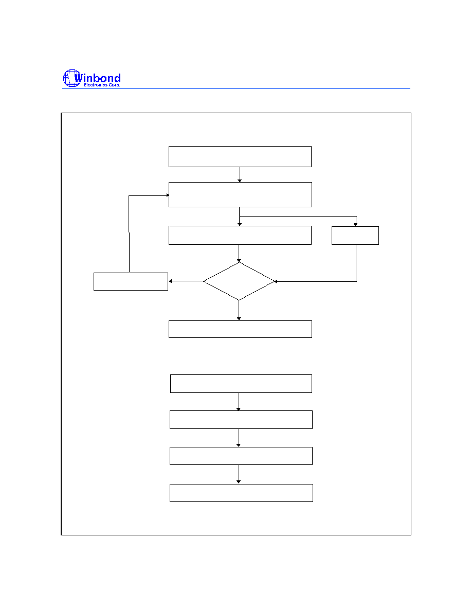
Embedded Programming Algorithm
Start
Write Program Command Sequence
(see below)
Increment Address
Programming Completed
5555H/AAH
2AAAH/55H
5555H/A0H
Program Address/Program Data
#Data Polling/ Toggle bit
Last Address
?
No
Yes
Program Command Sequence (Address/Command):
Pause T
BP
W39L512
Publication Release Date: July 9, 2002
- 11 - Revision A2
Embedded Erase Algorithm
Start
Write Erase Command Sequence
(see below)
Erasure Completed
#Data Polling or Toggle Bit
Successfully Completed
5555H/AAH
5555H/AAH
2AAAH/55H
2AAAH/55H
5555H/80H
5555H/10H
Chip Erase Command Sequence
(Address/Command):
5555H/AAH
5555H/AAH
2AAAH/55H
2AAAH/55H
5555H/80H
Page Address/50H
Individual Page Erase
(Address/Command):
Command Sequence
Pause T
EC
/T
PEC
W39L512
- 12 -
Embedded #Data Polling Algorithm
Start
Read Byte
(DQ0 - DQ7)
Address = VA
Pass
DQ7 = Data
?
Yes
No
VA = Byte address for programming
= Any of the page addresses within
the page being erased during page
erase operation
=Any of the device addresses being erased
during chip operation
Embedded Toggle Bit Algorithm
Start
Read Byte
(DQ0 - DQ7)
Address = Don't Care
DQ6 = Toggle
?
Yes
No
Pass
W39L512
Publication Release Date: July 9, 2002
- 13 - Revision A2
Boot Block Lockout Enable Flow Chart
Boot Block Lockout
Feature Set Flow
Load data AA
to
address 5555
Load data 55
to
address 2AAA
Load data 80
to
address 5555
Load data AA
to
address 5555
Load data 55
to
address 2AAA
Load data 70
to
address 5555
Pause 2 mS
Exit
70 to lcok 8K Boot Block
Load data XX
to
FFFF(XX) to lock Top Boot Block
0000(XX) to lock Bottom Boot Block
address FFFF/0 h
W39L512
- 14 -
Software Product Identification and Boot Block Lockout Detection Flow Chart
Product
Identification
Entry (1)
Load data 55
to
address 2AAA
Load data 90
to
address 5555
Pause 10 S
Product
Identification
and Boot Block
Lockout
Detection
Mode (3)
Read address = 0000
data = DA
Read address = 0001
Read address= 02/FFF2
for Bottom/Top
data: in DQ1 = "1" or "0"
for 8K Boot Block
(4)
Product
Identification Exit(6)
Load data 55
to
address 2AAA
Load data F0
to
address 5555
Normal Mode
(5)
(2)
(2)
Load data AA
to
address 5555
µ
Load data AA
to
address 5555
Pause 10 S
µ
data = 38
Notes for software product identification/boot block lockout detection:
(1) Data Format: DQ7
-
DQ0 (Hex); Address Format: A15
-
A0 (Hex)
(2) A1
-
A15 = V
IL
; manufacture code is read for A0 = V
IL
; device code is read for A0 = V
IH
.
(3) The device does not remain in identification and boot block lockout detection mode if power down.
(4) If the output data in DQ0 or DQ1= " 1 " the boot block programming lockout feature is activated; if the output data
in DQ0 or DQ1= " 0," the lockout feature is inactivated and the matched boot block can be programmed.
(5) The device returns to standard operation mode.
(6) Optional 1-byte cycle (write F0 hex at XXXX address) can be used to exit the product identification/boot block lockout
detection.
W39L512
Publication Release Date: July 9, 2002
- 15 - Revision A2
8. DC CHARACTERISTICS
Absolute maximum Ratings
PARAMETER
RATING
UNIT
Power Supply Voltage to V
SS
Potential
-2.0 to +4.6
V
Operating Temperature
0 to +70
∞
C
Storage Temperature
-65 to +125
∞
C
Voltage on Any Pin to Ground Potential Except A9
-2.0 to +4.6
V
Voltage on A9 Pin to Ground Potential
-2.0 to +13.0
V
Note: Exposure to conditions beyond those listed under Absolute maximum Ratings may adversely affect the life and reliability
of the device.
DC Operating Characteristics
(V
DD
= 3.3V
±
0.3V, V
SS
= 0V, T
A
= 0 to 70
∞
C)
LIMITS
PARAMETER
SYM.
TEST CONDITIONS
MIN. TYP. MAX.
UNIT
Power Supply Current
I
DD
#CE = #OE = V
IL
, #WE = V
IH
,
all DQs open, Address inputs = V
IL
/
V
IH
, at f = 5 MHz
-
10
20
mA
Standby V
DD
Current
(TTL input)
I
SB
1
#CE = V
IH
, all DQs open
Other inputs = V
IL
/V
IH
-
1
2
mA
Standby V
DD
Current
(CMOS input)
I
SB
2
#CE = V
DD
-0.3V, all DQs open
Other inputs = V
DD
-0.3V/ V
SS
-
15
50
µ
A
Input Leakage Current
I
LI
V
IN
= V
SS
to V
DD
-
-
1
µ
A
Output Leakage Current I
LO
V
OUT
= V
SS
to V
DD
-
-
1
µ
A
Input Low Voltage
V
IL
-
-0.3
-
0.8
V
Input High Voltage
V
IH
-
2.0
- V
DD
+0.5 V
Output Low Voltage
V
OL
I
OL
= 2.1 mA
-
-
0.45
V
Output High Voltage
V
OH
I
OH
= -0.4 mA
2.4
-
-
V
Pin Capacitance
(V
DD
= 3.3V, T
A
= 25
∞
C, f = 1 MHz)
PARAMETER
SYMBOL
CONDITIONS
TYP.
MAX.
UNIT
Input Capacitance
C
IN
V
IN
= 0V
6
8
pF
Output Capacitance
C
OUT
V
OUT
= 0V
10
12
pF
W39L512
- 16 -
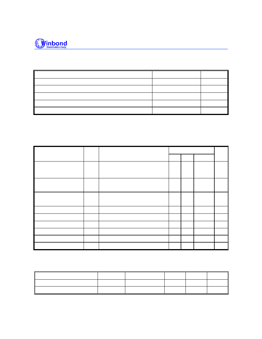
9. AC CHARACTERISTICS
AC Test Conditions
PARAMETER
CONDITIONS
Input Pulse Levels
0V to 3V
Input Rise/Fall Time
<5 nS
Input/Output Timing Level
1.5V/1.5V
Output Load
1 TTL Gate and C
L
= 30 pF
AC Test Load and Waveform
+3.3V
1.2K
2.1K
D
OUT
30 pF
(Including Jig and Scope)
Input
3V
0V
Test Point
Test Point
1.5V
1.5V
Output
W39L512
Publication Release Date: July 9, 2002
- 17 - Revision A2
AC Characteristics, continued
Read Cycle Timing Parameters
(V
DD
= 3.3V
±
0.3V, V
SS
= 0V, T
A
= 0 to 70
∞
C)
W39L512-70
W39L512-90
PARAMETER
SYM.
MIN.
MAX.
MIN.
MAX.
UNIT
Read Cycle Time
T
RC
70
-
90
-
nS
Chip Enable Access Time
T
CE
-
70
-
90
nS
Address Access Time
T
AA
-
70
-
90
nS
Output Enable Access Time
T
OE
-
35
-
45
nS
#CE Low to Active Output
T
CLZ
0
-
0
-
nS
#OE Low to Active Output
T
OLZ
0
-
0
-
nS
#CE High to High-Z Output
T
CHZ
-
25
-
25
nS
#OE High to High-Z Output
T
OHZ
-
25
-
25
nS
Output Hold from Address Change
T
OH
0
-
0
-
nS
Write Cycle Timing Parameters
PARAMETER
SYMBOL
MIN.
TYP.
MAX.
UNIT
Address Setup Time
T
AS
0
-
-
nS
Address Hold Time
T
AH
40
-
-
nS
#WE and #CE Setup Time
T
CS
0
-
-
nS
#WE and #CE Hold Time
T
CH
0
-
-
nS
#OE High Setup Time
T
OES
0
-
-
nS
#OE High Hold Time
T
OEH
0
-
-
nS
#CE Pulse Width
T
CP
100
-
-
nS
#WE Pulse Width
T
WP
100
-
-
nS
#WE High Width
T
WPH
100
-
-
nS
Data Setup Time
T
DS
40
-
-
nS
Data Hold Time
T
DH
10
-
-
nS
Byte Programming Time
T
BP
-
35
50
µ
S
Chip Erase Cycle Time
T
EC
-
50
100
mS
Page Erase Cycle Time
T
EP
-
12.5
25
mS
Note: All AC timing signals observe the following guidelines for determining setup and hold times:
(a) High level signal's reference level is V
IH
and (b) low level signal's reference level is V
IL
.
W39L512
- 18 -
AC Characteristics, continued
Power-up Timing
PARAMETER
SYMBOL
TYPICAL
UNIT
Power-up to Read Operation
T
PU
. READ
100
µ
S
Power-up to Write Operation
T
PU
. WRITE
5
mS
Data Polling and Toggle Bit Timing Parameters
W39L512
-70
W39L512
-90
PARAMETER
SYM.
MIN.
MAX.
MIN.
MAX.
UNIT
#OE to Data Polling Output Delay
T
OEP
-
35
-
45
nS
#CE to Data Polling Output Delay
T
CEP
-
70
-
90
nS
#OE to Toggle Bit Output Delay
T
OET
-
35
-
45
nS
#CE to Toggle Bit Output Delay
T
CET
-
70
-
90
nS
W39L512
Publication Release Date: July 9, 2002
- 19 - Revision A2
10. TIMING WAVEFORMS
Read Cycle Timing Diagram
Address A15-0
DQ7-0
Data Valid
Data Valid
High-Z
#CE
#OE
#WE
T
RC
V
IH
T
CLZ
T
OLZ
T
OE
T
CE
T
OH
T
AA
T
CHZ
T
OHZ
High-Z
#WE Controlled Command Write Cycle Timing Diagram
Address A15-0
DQ7-0
Data Valid
#CE
#OE
#WE
T
AS
T
CS
T
OES
T
AH
T
CH
T
OEH
T
WPH
T
WP
T
DS
T
DH
W39L512
- 20 -
Timing Waveforms, continued
#CE Controlled Command Write Cycle Timing Diagram
High Z
Data Valid
#CE
#OE
#WE
DQ7-0
T
AS
T
AH
T
CPH
T
OEH
T
DH
T
DS
T
CP
T
OES
Address A15-0
Chip Erase Timing Diagram
SB2
SB1
SB0
Address A15-0
DQ7-0
#CE
#OE
#WE
SB3
SB4
SB5
Internal Erase starts
Six-byte code for 3.3V-only software
chip erase
T
WP
T
WPH
5555
2AAA
5555
5555
2AAA
5555
AA
55
80
AA
55
10
T
EC
W39L512
Publication Release Date: July 9, 2002
- 21 - Revision A2
Timing Waveforms, continued
Page Erase Timing Diagram
SB2
SB1
SB0
Address A15-0
DQ7-0
#CE
#OE
#WE
SB3
SB4
SB5
Internal Erase starts
Six-byte commands for 3.3V-only
Page Erase
T
WP
T
WPH
T
EP
5555
2AAA
5555
5555
2AAA
PA
AA
55
80
AA
55
50
PA = Page Address
Please refer to page 9 for detail information
#DATA Polling Timing Diagram
Address A15-0
DQ7
#WE
#OE
#CE
X
# X
# X
X
T
CEP
T
OEH
T
OEP
T
OES
T
EC
T
BP or
An
An
An
An
W39L512
- 22 -
Timing Waveforms, continued
Toggle Bit Timing Diagram
Address A15-0
DQ6
#CE
#OE
#WE
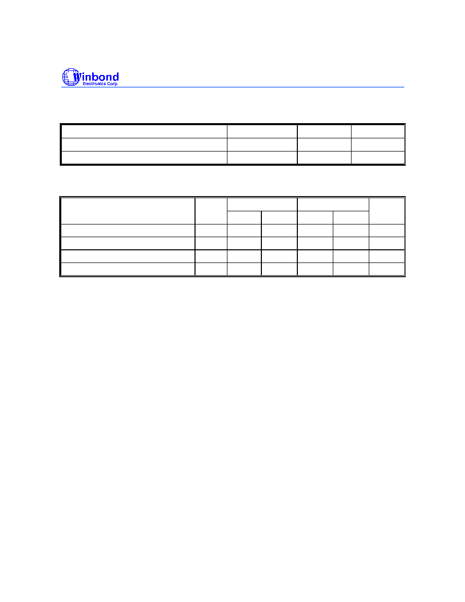
T
OEH
T
OES
T
BP or
T
EC
W39L512
Publication Release Date: July 9, 2002
- 23 - Revision A2
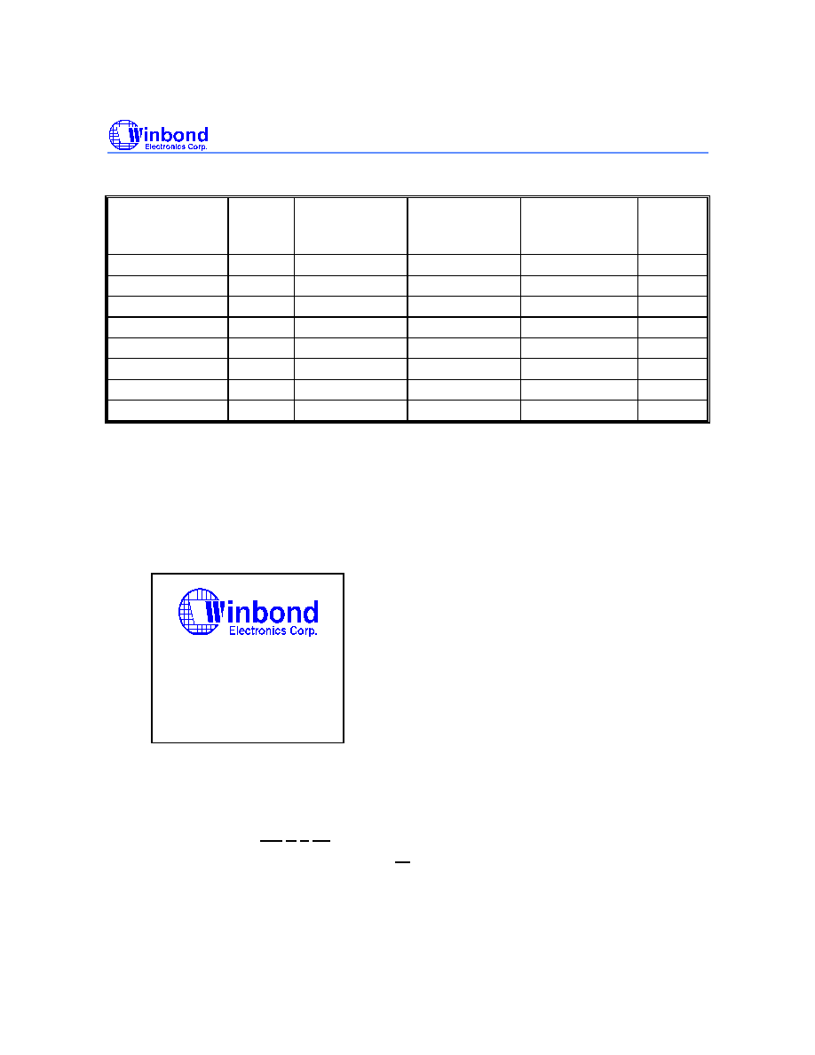
11. ORDERING INFORMATION
PART NO.
ACCESS
TIME
(nS)
POWER SUPPLY
CURRENT MAX.
(mA)
STANDBY V
DD
CURRENT MAX.
(mA)
PACKAGE
CYCLE
W39L512P-70
70
20
2
32-pin PLCC
1K
W39L512P-90
90
20
2
32-pin PLCC
1K
W39L512Q-70
70
20
2
32-pin STSOP
1K
W39L512Q-90
90
20
2
32-pin STSOP
1K
W39L512P-70B
70
20
2
32-pin PLCC
10K
W39L512P-90B
90
20
2
32-pin PLCC
10K
W39L512Q-70B
70
20
2
32-pin STSOP
10K
W39L512Q-90B
90
20
2
32-pin STSOP
10K
Notes:
1. Winbond reserves the right to make changes to its products without prior notice.
2. Purchasers are responsible for performing appropriate quality assurance testing on products intended for use in
applications where personal injury might occur as a consequence of product failure.
12. HOW TO READ THE TOP MARKING
Example: The top marking of 32-pin PLCC W39L512P-70
1
st
line: winbond logo
2
nd
line: the part number: W39L512P-70
3
rd
line: the lot number
4
th
line: the tracking code: 149 O B SA
149: Packages made in '01, week 49
O: Assembly house ID: A means ASE, O means OSE, ...etc.
B: IC revision; A means version A, B means version B, ...etc.
SA: Process code
W39L512P-70
2138977A-A12
149OBSA
W39L512
- 24 -
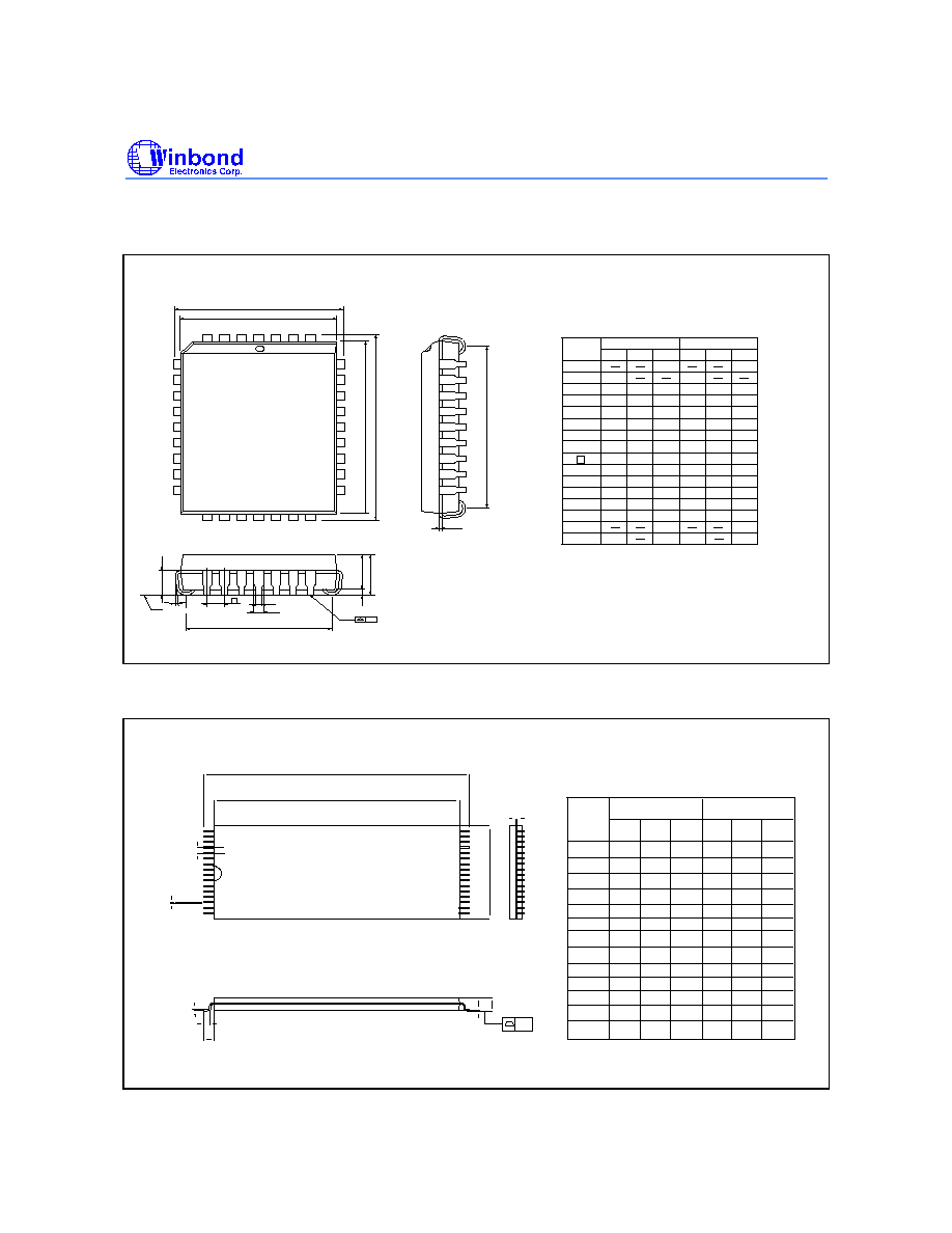
13. PACKAGE DIMENSIONS
32-pin PLCC
L
c
1
b
2
A
H
E
E
e
b
D H
D
y
A
A
1
Seating Plane
E
G
G
D
1
13
14
20
29
32
4
5
21
30
Notes:
1. Dimensions D & E do not include interlead flash.
2. Dimension b1 does not include dambar protrusion/intrusion.
3. Controlling dimension: Inches.
4. General appearance spec. should be based on final
visual inspection sepc.
Symbol
Min.
Nom.
Max.
Max.
Nom.
Min.
Dimension in Inches
Dimension in mm
A
b
c
D
e
H
E
L
y
A
A
1
2
E
b
1
G
D
3.56
0.50
2.80
2.67
2.93
0.71
0.66
0.81
0.41
0.46
0.56
0.20
0.25
0.35
13.89
13.97
14.05
11.35
11.43
11.51
1.27
H
D
G
E
12.45
12.95
13.46
9.91
10.41
10.92
14.86
14.99
15.11
12.32
12.45
12.57
1.91
2.29
0.004
0.095
0.090
0.075
0.495
0.490
0.485
0.595
0.590
0.585
0.430
0.410
0.390
0.530
0.510
0.490
0.050
0.453
0.450
0.447
0.553
0.550
0.547
0.014
0.010
0.008
0.022
0.018
0.016
0.032
0.026
0.028
0.115
0.105
0.110
0.020
0.140
1.12
1.42
0.044
0.056
0
∞
10
∞
10
∞
0
∞
0.10
2.41
32-pin STSOP (8 x 14 mm)
Min.
Dimension in Inches
Nom. Max.
Min.
Nom. Max.
Symbol
1.20
0.05
0.15
1.05
1.00
0.95
0.17
0.10
0.50
0.00
0
0.22
0.27
-----
0.21
12.40
8.00
14.00
0.50
0.60
0.70
0.80
0.10
3
5
0.047
0.006
0.041
0.040
0.035
0.007
0.009
0.010
0.004
-----
0.008
0.488
0.315
0.551
0.020
0.020
0.024
0.028
0.031
0.000
0.004
0
3
5
0.002
A
A
b
c
D
E
e
L
L
Y
1
1
2
A
H
D
Dimension in mm
A
A
A
2
1
L
L
1
Y
E
H
D
D
c
£c
b
e
W39L512
Publication Release Date: July 9, 2002
- 25 - Revision A2
14. VERSION HISTORY
VERSION
DATE
PAGE
DESCRIPTION
A1
June 4, 2002
-
Initial Issued
A2
July 9, 2002
11
Remove Block Erase from the Embedded Erase
Algorithm
12
Correct Embedded #Data Polling Algorithm
Headquarters
No. 4, Creation Rd. III,
Science-Based Industrial Park,
Hsinchu, Taiwan
TEL: 886-3-5770066
FAX: 886-3-5665577
http://www.winbond.com.tw/
Taipei Office
TEL: 886-2-8177-7168
FAX: 886-2-8751-3579
Winbond Electronics Corporation America
2727 North First Street, San Jose,
CA 95134, U.S.A.
TEL: 1-408-9436666
FAX: 1-408-5441798
Winbond Electronics (H.K.) Ltd.
No. 378 Kwun Tong Rd.,
Kowloon, Hong Kong
FAX: 852-27552064
Unit 9-15, 22F, Millennium City,
TEL: 852-27513100
Please note that all data and specifications are subject to change without notice.
All the trade marks of products and companies mentioned in this data sheet belong to their respective owners.
Winbond Electronics (Shanghai) Ltd.
200336 China
FAX: 86-21-62365998
27F, 2299 Yan An W. Rd. Shanghai,
TEL: 86-21-62365999
Winbond Electronics Corporation Japan
Shinyokohama Kohoku-ku,
Yokohama, 222-0033
FAX: 81-45-4781800
7F Daini-ueno BLDG, 3-7-18
TEL: 81-45-4781881
9F, No.480, Rueiguang Rd.,
Neihu Chiu, Taipei, 114,
Taiwan, R.O.C.