
W39V040FA
512K
◊ 8 CMOS FLASH MEMORY
WITH FWH INTERFACE
Publication Release Date: December 19, 2002
- 1 -
Revision A2
1. GENERAL DESCRIPTION
The W39V040FA is a 4-megabit, 3.3-volt only CMOS flash memory organized as 512K
◊ 8 bits. For
flexible erase capability, the 4Mbits of data are divided into 8 uniform sectors of 64 Kbytes, which are
composed of 16 smaller even pages with 4 Kbytes. The device can be programmed and erased in-
system with a standard 3.3V power supply. A 12-volt VPP is not required. The unique cell architecture
of the W39V040FA results in fast program/erase operations with extremely low current consumption.
This device can operate at two modes, Programmer bus interface mode and FWH bus interface
mode. As in the Programmer interface mode, it acts like the traditional flash but with a multiplexed
address inputs. But in the FWH interface mode, this device complies with the Intel FWH specification.
The device can also be programmed and erased using standard EPROM programmers.
2. FEATURES
∑
Single 3.3-volt operations:
- 3.3-volt read
- 3.3-volt erase
- 3.3-volt program
∑
Fast Program operation:
- Byte-by-Byte programming: 35 µS (typ.)
∑
Fast erase operation:
- Chip erase 100 mS (max.)
- Sector erase 25 mS (max.)
- Page erase 25 mS (max.)
∑
Fast Read access time: Tkq 11 nS
∑
Endurance: 10K cycles (typ.)
∑
Twenty-year data retention
∑
8 Even sectors with 64K bytes each, which is
composed of 16 flexible pages with 4K bytes
∑
Any individual sector or page can be erased
∑
Hardware protection:
- Optional 16K byte or 64K byte Top Boot
Block with lockout protection
- #TBL & #WP support the whole chip
hardware protection
∑
Flexible 4K-page size can be used as
Parameter Blocks
∑
Low power consumption
- Active current: 12.5 mA (typ. for FWH mode)
∑
Automatic program and erase timing with
internal
V
PP
generation
∑
End of program or erase detection
- Toggle bit
- Data polling
∑
Latched address and data
∑
TTL compatible I/O
∑
Available packages: 32L PLCC, 32L STSOP,
40L TSOP (10 x 20 mm)
W39V040FA
- 2 -
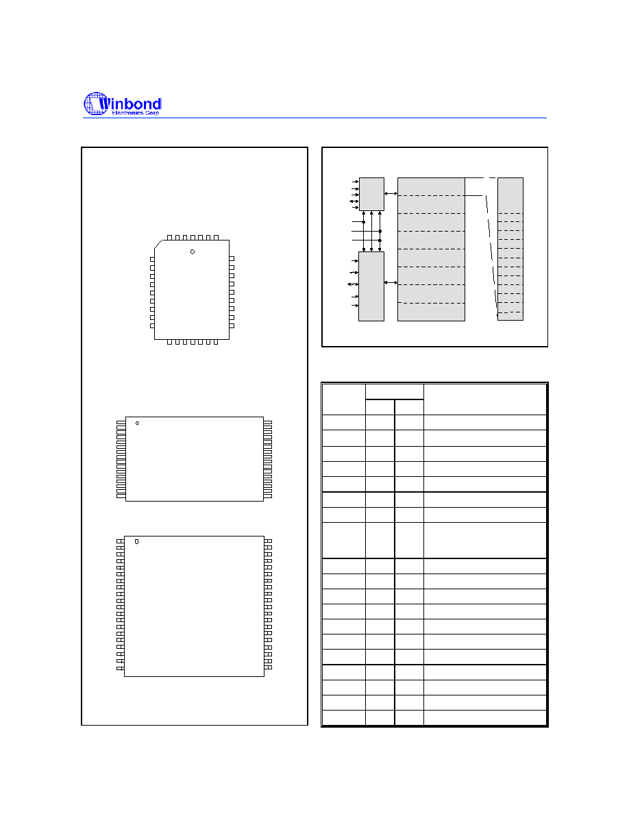
3. PIN CONFIGURATIONS
5
6
7
9
10
11
12
13
29
28
27
26
25
24
23
22
21
30
31
32
1
2
3
4
8
20
19
18
17
16
15
14
D
Q
1
^
F
W
H
1
v
V
S
S
D
Q
6
^
R
S
V
v
#
R
E
S
E
T
V
D
D
R
/
#
C
^
C
L
K
v
A
9
^
F
G
P
I
3
v
32L PLCC
A
1
0
^
F
G
P
I
4
v
N
C
DQ0(FWH0)
A7(FGPI1)
A6(FGPI0)
A4(#TBL)
A3(ID3)
A2(ID2)
A1(ID1)
A0(ID0)
A5(#WP)
IC
DQ7(RSV)
#WE(FWH4)
#OE(#INIT)
NC
A
8
^
F
G
P
I
2
v
D
Q
2
^
F
W
H
2
v
D
Q
3
^
F
W
H
3
v
D
Q
4
^
R
S
V
v
D
Q
5
^
R
S
V
v
V
SS
NC
V
DD
NC
1
2
3
4
5
6
7
8
9
10
11
12
13
14
15
16
32
31
30
29
28
27
26
25
32L STSOP
24
23
22
21
#WE(FWH4)
DQ4(RSV)
DQ3(FWH3)
DQ7(RSV)
DQ6(RSV)
#OE(#INIT)
DQ5(RSV)
20
19
18
17
A3(ID3)
IC
R/#C(CLK)
NC
V
DD
A10(FGPI4)
NC
A9(FGPI3)
A8(FGPI2)
#RESET
A7(FGPI1)
A6(FGPI0)
A2(ID2)
A1(ID1)
A0(ID0)
DQ2(FWH2)
DQ1(FWH1)
DQ0(FWH0)
A5(#WP)
A4(#TBL)
V
SS
V
SS
V
DD
NC
NC
1
10
40L TSOP
40
39
38
37
36
35
34
33
32
31
30
29
28
27
26
25
NC
VDD
CLK
A9(FGPI3)
A8(FGPI2)
NC
VSS
VSS
VDD
DQ7(RSV)
DQ6(RSV)
VDD
VSS
NC
IC
A4(#TBL)
A5(#WP)
2
3
4
5
6
7
8
9
11
12
13
14
15
16
18
19
17
20
24
21
22
23
NC
NC
NC
A10(FGPI4)
NC
#RESET
NC
NC
A7(FGPI1)
A6(FGPI0)
DQ5(RSV)
DQ4(RSV)
#WE(FWH4)
A0(ID0)
A1(ID1)
A2(ID2)
A3(ID3)
DQ3(FWH3)
DQ2(FWH2)
DQ1(FWH1)
DQ0(FWH0)
NC
#OE(#INIT)
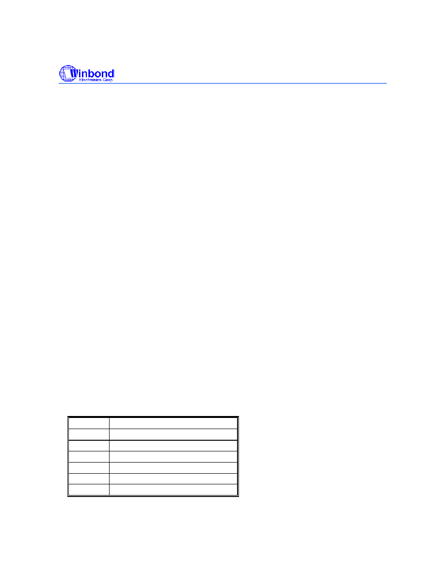
4. BLOCK DIAGRAM
Program-
mer
Interface
7FFFF
00000
20000
1FFFF
10000
0FFFF
#RESET
IC
A[10:0]
DQ[7:0]
#OE
#WE
R/#C
FWH
Interface
CLK
FWH4
FWH[3:0]
70000
6FFFF
BOOT BLOCK 64K BYTES
MAIN MEMORY BLOCK6
64K BYTES
MAIN MEMORY BLOCK5
64K BYTES
MAIN MEMORY BLOCK4
64K BYTES
MAIN MEMORY BLOCK3
64K BYTES
MAIN MEMORY BLOCK2
64K BYTES
MAIN MEMORY BLOCK0
64K BYTES
30000
2FFFF
40000
3FFFF
50000
4FFFF
MAIN MEMORY BLOCK1
64K BYTES
60000
5FFFF
#INIT
4K Page
4K Page
4K Page
4K Page
4K Page
4K Page
4K Page
4K Page
4K Page
4K Page
4K Page
4K Page
Optional
16KBytes
as
Boot Block
7FFFF
7C000
7BFFF
70000
#WP
#TBL
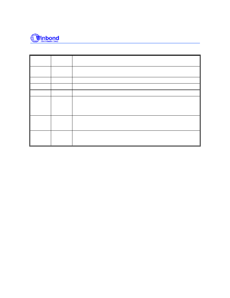
5. PIN DESCRIPTION
INTERFACE
SYM.
PGM FWH
PIN NAME
IC
*
*
Interface Mode Selection
#RESET * * Reset
#INIT *
Initialize
#TBL
*
Top Boot Block Lock
#WP
*
Write
Protect
CLK *
CLK
Input
FGPI[4:0]
*
General Purpose Inputs
ID[3:0] *
Identification Inputs They
Are Internal Pull Down to
Vss
FWH[3:0] * Address/Data
Inputs
FWH4
*
FWH Cycle Initial
R/#C * Row/Column
Select
A[10:0] * Address
Inputs
DQ[7:0] * Data
Inputs/Outputs
#OE *
Output
Enable
#WE * Write
Enable
V
DD
* *
Power
Supply
V
SS
* *
Ground
RSV * *
Reserved
Pins
NC
*
*
No Connection

W39V040FA
Publication Release Date: December 19, 2002
- 3 -
Revision A2
6. FUNCTIONAL DESCRIPTION
Interface Mode Selection and Description
This device can operate in two interface modes, one is Programmer interface mode, and the other is
FWH interface mode. The IC pin of the device provides the control between these two interface
modes. These interface modes need to be configured before power up or return from #RESET
.
When
IC pin is set to high state, the device will be in the Programmer mode; while the IC pin is set to low
state (or leaved no connection), it will be in the FWH mode. In Programmer mode, this device just
behaves like traditional flash parts with 8 data lines. But the row and column address inputs are
multiplexed. The row address are mapped to the higher internal address A[18:11]. And the column
address are mapped to the lower internal address A[10:0]. For FWH mode, it complies with the FWH
Interface Specification. Through the FWH[3:0] and FWH4 to communicate with the system chipset .
Read (Write) Mode
In Programmer interface mode, the read (write) operation of the W39V040FA is controlled by #OE
(#WE). The #OE (#WE) is held low for the host to obtain (write) data from (to) the outputs (inputs).
#OE is the output control and is used to gate data from the output pins. The data bus is in high
impedance state when #OE is high. As for in the FWH interface mode, the read or write is determined
by the "bit 0 & bit 1 of START CYCLE ". Refer to the FWH cycle definition and timing waveforms for
further details.
Reset Operation
The #RESET input pin can be used in some application. When #RESET pin is at high state, the
device is in normal operation mode. When #RESET pin is at low state, it will halt the device and all
outputs will be at high impedance state. As the high state re-asserted to the #RESET pin, the device
will return to read or standby mode, it depends on the control signals.
Boot Block Operation and Hardware Protection at Initial- #TBL & #WP
There are two alternatives to set the boot block. Either 16K-byte or 64K-byte in the top location of this
device can be locked as boot block, which can be used to store boot codes. It is located in the last
16K/64K bytes of the memory with the address range from 7C000(hex)/70000(hex) to 7FFFF(hex).
See Command Codes for Boot Block Lockout Enable for the specific code. Once this feature is set the
data for the designated block cannot be erased or programmed (programming lockout), other memory
locations can be changed by the regular programming method.
Besides the software method, there is a hardware method to protect the top boot block and other
sectors. Before power on programmer, tie the #TBL pin to low state and then the top boot block will
not be programmed/erased. If #WP pin is tied to low state before power on, the other sectors will not
be programmed/erased.
In order to detect whether the boot block feature is set on or not, users can perform software
command sequence: enter the product identification mode (see Command Codes for
Identification/Boot Block Lockout Detection for specific code), and then read from address
7FFF2(hex). If the DQ0/DQ1 output data is "1," the 64Kbytes/16Kbytes boot block programming
lockout feature will be activated; if the DQ0/DQ1 output data is "0," the lockout feature will be
inactivated and the boot block can be erased/programmed. But the hardware protection will override
the software lock setting, i.e., while the #TBL pin is trapped at low state, the top boot block cannot be

W39V040FA
- 4 -
programmed/erased whether the output data, DQ0/DQ1 at the address 7FFF2, is "0" or "1". The #TBL
will lock the whole 64Kbytes top boot block, it will not partially lock the 16Kbytes boot block. You can
check the DQ2/DQ3 at the address 7FFF2 to see whether the #TBL/#WP pin
is in low or high state. If
the DQ2 is "0", it means the #TBL
pin is tied to high state. In such condition, whether boot block can
be programmed/erased or not will depend on software setting. On the other hand, if the DQ2 is "1", it
means the #TBL
pin is tied to low state, then boot block is locked no matter how the software is set.
Like the DQ2, the DQ3 inversely mirrors the #WP state. If the DQ3 is "0", it means the #WP
pin is in
high state, then all the sectors except the boot block can be programmed/erased. On the other hand, if
the DQ3 is "1", then all the sectors except the boot block are programmed/erased inhibited.
To return to normal operation, perform a three-byte command sequence (or an alternate single-byte
command) to exit the identification mode. For the specific code, see Command Codes for
Identification/Boot Block Lockout Detection.
Chip Erase Operation
The chip-erase mode can be initiated by a six-byte command sequence. After the command loading
cycle, the device enters the internal chip erase mode, which is automatically timed and will be
completed within fast 100 mS (max). The host system is not required to provide any control or timing
during this operation. If the boot block programming lockout is activated, only the data in the other
memory sectors will be erased to FF(hex) while the data in the boot block will not be erased (remains
as the same state before the chip erase operation). The entire memory array will be erased to FF(hex)
by the chip erase operation if the boot block programming lockout feature is not activated. The device
will automatically return to normal read mode after the erase operation completed. Data polling and/or
Toggle Bits can be used to detect end of erase cycle.
Sector/Page Erase Command
Sector/page erase is a six bus cycles operation. There are two "unlock" write cycles, followed by
writing the "set-up" command. Two more "unlock" write cycles then follows by the sector/page erase
command. The sector/page address (any address location within the desired sector/page) is latched
on the falling edge of #WE, while the command (30H/50H) is latched on the rising edge of #WE.
Sector/page erase does not require the user to program the device prior to erase. When erasing a
sector/page or sectors/pages the remaining unselected sectors/pages are not affected. The system is
not required to provide any controls or timings during these operations.
The automatic sector/page erase begins after the erase command is completed, right from the rising
edge of the #WE pulse for the last sector/page erase command pulse and terminates when the data
on DQ7, Data Polling, is "1" at which time the device returns to the read mode. Data Polling must be
performed at an address within any of the sectors/pages being erased.
Refer to the Erase Command flow Chart using typical command strings and bus operations.
Program Operation
The W39V040FA is programmed on a byte-by-byte basis. Program operation can only change logical
data "1" to logical data "0." The erase operation, which changed entire data in main memory and/or
boot block from "0" to "1", is needed before programming.
The program operation is initiated by a 4-byte command cycle (see Command Codes for Byte
Programming). The device will internally enter the program operation immediately after the byte-
program command is entered. The internal program timer will automatically time-out (50
µS max. -
T
BP
) once it is completed and then return to normal read mode. Data polling and/or Toggle Bits can be
used to detect end of program cycle.
W39V040FA
Publication Release Date: December 19, 2002
- 5 -
Revision A2
Hardware Data Protection
The integrity of the data stored in the W39V040FA is also hardware protected in the following ways:
(1) Noise/Glitch Protection: A #WE pulse of less than 15 nS in duration will not initiate a write cycle.
(2) V
DD
Power Up/Down Detection: The programming and read operation are inhibited when V
DD
is
less than 1.5V typical.
(3) Write Inhibit Mode: Forcing #OE low or #WE high will inhibit the write operation. This prevents
inadvertent writes during power-up or power-down periods.
(4) V
DD
power-on delay: When V
DD
has reached its sense level, the device will automatically time-out
5 mS before any write (erase/program) operation.
Data Polling (DQ
7
)- Write Status Detection
The W39V040FA includes a data polling feature to indicate the end of a program or erase cycle.
When the W39V040FA is in the internal program or erase cycle, any attempts to read DQ
7
of the last
byte loaded will receive the complement of the true data. Once the program or erase cycle is
completed, DQ
7
will show the true data. Note that DQ
7
will show logical "0" during the erase cycle,
and when erase cycle has been completed it becomes logical "1" or true data.
Toggle Bit (DQ
6
)- Write Status Detection
In addition to data polling, the W39V040FA provides another method for determining the end of a
program cycle. During the internal program or erase cycle, any consecutive attempts to read DQ
6
will
produce alternating 0's and 1's. When the program or erase cycle is completed, this toggling between
0's and 1's will stop. The device is then ready for the next operation.
Register
There are three kinds of registers on this device, the General Purpose Input Registers, the Block Lock
Control Registers and Product Identification Registers. Users can access these registers through
respective address in the 4Gbytes memory map. There are detail descriptions in the sections below.
General Purpose Inputs Register
This register reads the FGPI[4:0] pins on the W39V040FA.This is a pass-through register which can
read via memory address FFBC0100(hex). Since it is pass-through register, there is no default value.
GPI Register Table
BIT FUNCTION
7
- 5
Reserved
4
Read FGPI4 pin status
3
Read FGPI3 pin status
2
Read FGPI2 pin status
1
Read FGPI1 pin status
0
Read FGPI0 pin status
W39V040FA
- 6 -
Block Locking Registers
This part provides 8 even 64Kbytes blocks, and each block can be locked by register control. These
control registers can be set or clear through memory address. Below is the detail description.
Block Locking Registers type and access memory map Table
REGISTERS
REGISTERS
TYPE
CONTROL
BLOCK
DEVICE PHYSICAL
ADDRESS
4GBYTES SYSTEM
MEMORY ADDRESS
BLR7
R/W
7
7FFFFh ≠ 70000h
FFBF0002h
BLR6
R/W
6
6FFFFh ≠ 60000h
FFBE0002h
BLR5
R/W
5
5FFFFh ≠ 50000h
FFBD0002h
BLR4
R/W
4
4FFFFh ≠ 40000h
FFBC0002h
BLR3
R/W
3
3FFFFh ≠ 30000h
FFBB0002h
BLR2
R/W
2
2FFFFh ≠ 20000h
FFBA0002h
BLR1
R/W
1
1FFFFh ≠ 10000h
FFB90002h
BLR0
R/W
0
0FFFFh ≠ 00000h
FFB80002h
Block Locking Register Bits Function Table
BIT FUNCTION
7 ≠ 3
Reserved
2
Read Lock
1: Prohibit to read in the block where set
0: Normal read operation in the block where clear. This is default state.
1
Lock Down
1: Prohibit further to set or clear the Read Lock or Write Lock bits. This Lock Down
Bit can only be set not clear. Only the device is reset or re-powered, the Lock
Down Bit is cleared.
0: Normal operation for Read Lock or Write Lock. This is the default state.
0
Write Lock
1: Prohibited to write in the block where set. This is default state.
0: Normal programming/erase operation in the block where clear.
Register Based Block Locking Value Definitions Table
BIT [7:3]
BIT 2
BIT 1
BIT 0
RESULT
00000 0 0 0
Full
Access.
00000 0 0 1
Write
Lock. Default State.
00000
0
1
0
Locked Open (Full Access, Lock Down).
00000
0
1
1
Write Locked, Locked Down.
00000 1 0 0
Read
Locked.
00000
1
0
1
Read & Write Locked.
00000
1
1
0
Read Locked, Locked Down.
00000
1
1
1
Read & Write Locked, Locked Down.
W39V040FA
Publication Release Date: December 19, 2002
- 7 -
Revision A2
Read Lock
Any attempt to read the data of read locked block will result in "00." The default state of any block is
unlocked upon power up. User can clear or set the write lock bit anytime as long as the lock down bit
is not set.
Write Lock
This is the default state of blocks upon power up. Before any program or erase to the specified block,
user should clear the write lock bit first. User can clear or set the write lock bit anytime as long as the
lock down bit is not set. The write lock function is in conjunction with the hardware protect pins, #WP &
TBL. When hardware protect pins are enabled, it will override the register block locking functions and
write lock the blocks no matter how the status of the register bits. Reading the register bit will not
reflect the status of the #WP or #TBL pins.
Lock Down
The default state of lock down bit for any block is unlocked. This bit can be set only once; any further
attempt to set or clear is ignored. Only the reset from #RESET or #INIT can clear the lock down bit.
Once the lock down bit is set for a block, then the write lock bit & read lock bit of that block will not be
set or cleared, and keep its current state.
Product Identification Registers
In the FWH interface mode, a read from FFBC, 0000(hex) can output the manufacturer code,
DA(hex). A read from FFBC, 0001(hex) can output the device code 34(hex).
There is an alternative software method (six commands bytes) to read out the Product Identification in
both the Programmer interface mode and the FWH interface mode. Thus, the programming equipment
can automatically matches the device with its proper erase and programming algorithms.
In the software access mode, a six-byte (or JEDEC 3-byte) command sequence can be used to
access the product ID for programmer interface mode. A read from address 0000(hex) outputs the
manufacturer code, DA(hex). A read from address 0001(hex) outputs the device code, 34(hex)." The
product ID operation can be terminated by a three-byte command sequence or an alternate one-byte
command sequence (see Command Definition table for detail).
Table of Operating Mode
Operating Mode Selection - Programmer Mode
PINS
MODE
#OE
#WE
#RESET
ADDRESS DQ.
Read V
IL
V
IH
V
IH
AIN Dout
Write V
IH
V
IL
V
IH
AIN Din
Standby X
X
V
IL
X
High
Z
V
IL
X V
IH
X
High
Z/DOUT
Write Inhibit
X V
IH
V
IH
X
High
Z/DOUT
Output Disable
V
IH
X V
IH
X
High
Z
W39V040FA
- 8 -
Operating Mode Selection - FWH Mode
Operation modes in FWH interface mode are determined by "START Cycle" when it is selected.
When it is not selected, its outputs (FWH[3:0]) will be disable. Please reference to the "FWH Cycle
Definition".
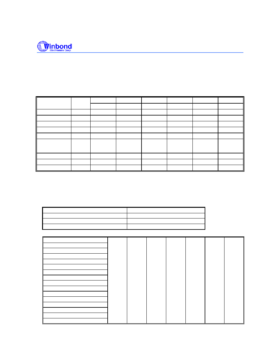
Table of Command Definition
COMMAND
NO. OF
1ST CYCLE
2ND CYCLE
3RD CYCLE
4TH CYCLE
5TH CYCLE
6TH CYCLE
DESCRIPTION
Cycles (1)
Addr. Data
Addr. Data
Addr. Data Addr.
Data Addr.
Data Addr.
Data
Read
1 A
IN
D
OUT
Chip Erase
6
5555 AA
2AAA 55
5555 80
5555 AA
2AAA 55
5555 10
Sector Erase
6
5555 AA
2AAA 55
5555 80
5555 AA
2AAA 55
SA
(5)
30
Page Erase
6
5555 AA
2AAA 55
5555 80
5555 AA
2AAA 55
PA
(6)
50
Byte Program
4
5555 AA
2AAA 55
5555 A0
A
IN
D
IN
Top Boot Block
Lockout ≠
64K/16KByte
6
5555 AA
2AAA 55
5555 80
5555 AA
2AAA 55
5555 40/70
Product ID Entry
3
5555 AA
2AAA 55
5555 90
Product ID Exit
(4)
3
5555 AA
2AAA 55
5555 F0
Product ID Exit
(4)
1
XXXX
F0
Notes:
1. The cycle means the write command cycle not the FWH clock cycle.
2. The Column Address / Row Address are mapped to the Low / High order Internal Address. i.e. Column Address
A[10:0] are mapped to the internal A[10:0], Row Address A[7:0] are mapped to the internal A[18:11]
3. Address Format: A14
-A0 (Hex); Data Format: DQ7-DQ0 (Hex)
4. Either one of the two Product ID Exit commands can be used.
5. SA: Sector Address
SA = 7XXXXh for Unique Sector7 (Boot Sector)
SA = 3XXXXh for Unique Sector3
SA = 6XXXXh for Unique Sector6
SA = 2XXXXh for Unique Sector2
SA = 5XXXXh for Unique Sector5
SA = 1XXXXh for Unique Sector1
SA = 4XXXXh for Unique Sector4
SA = 0XXXXh for Unique Sector0
6. PA : Page Address
PA = 7FXXXh for Page 15 in Sector 7
PA = 7EXXXh for Page 14 in Sector 7
PA = 7DXXXh for Page 13 in Sector 7
PA = 7CXXXh for Page 12 in Sector 7
PA = 7BXXXh for Page 11 in Sector 7
PA = 7AXXXh for Page 10 in Sector 7
PA = 79XXXh for Page 9 in Sector 7
PA = 78XXXh for Page 8 in Sector 7
PA = 77XXXh for Page 7 in Sector 7
PA = 76XXXh for Page 6 in Sector 7
PA = 75XXXh for Page 5 in Sector 7
PA = 74XXXh for Page 4 in Sector 7
PA = 73XXXh for Page 3 in Sector 7
PA = 72XXXh for Page 2 in Sector 7
PA = 71XXXh for Page 1 in Sector 7
PA = 70XXXh for Page 0 in Sector 7
PA =
6FXXXh
to
60XXXh
for
Page 15
to
Page 0
In
Sector 6
(Reference
to the
first
column)
PA =
5FXXXh
to
50XXXh
for
Page 15
to
Page 0
In
Sector 5
(Reference
to the
first
column)
PA =
4FXXXh
to
40XXXh
for
Page 15
to
Page 0
In
Sector 4
(Reference
to the
first
column)
PA =
3FXXXh
to
30XXXh
for
Page 15
to
Page 0
In
Sector 3
(Reference
to the
first
column)
PA =
2FXXXh
to
20XXXh
for
Page 15
to
Page 0
In
Sector 2
(Reference
to the
first
column)
PA =
1FXXXh
to
10XXXh
for
Page 15
to
Page 0
In
Sector 1
(Reference
to the
first
column)
PA =
0FXXXh
to
00XXXh
for
Page 15
to
Page 0
In
Sector 0
(Reference
to the
first
column)
W39V040FA
Publication Release Date: December 19, 2002
- 9 -
Revision A2
FWH Cycle Definition
FIELD
NO. OF
CLOCKS
DESCRIPTION
START 1
"1101b" indicates FWH Memory Read cycle; while "1110b" indicates FWH
Memory Write cycle. 0000b" appears on FWH bus to indicate the initial
IDSEL
1
This one clock field indicates which FWH component is being selected.
MSIZE
1
Memory Size. There is always show "0000b" for single byte access.
TAR
2
Turned Around Time
ADDR 7
Address Phase for Memory Cycle. FWH supports the 28 bits address
protocol. The addresses transfer most significant nibble first and least
significant nibble last. (i.e. Address[27:24] on FWH[3:0] first, and
Address[3:0] on FWH[3:0] last.)
SYNC N
Synchronous to add wait state. "0000b" means Ready, "0101b" means
Short Wait, "0110b" means Long Wait, "1001b" for DMA only, "1010b"
means error, and other values are reserved.
DATA 2
Data Phase for Memory Cycle. The data transfer least significant nibble
first and most significant nibble last. (i.e. DQ[3:0] on FWH[3:0] first, then
DQ[7:4] on FWH[3:0] last.)

W39V040FA
- 10 -
Embedded Programming Algorithm
Start
Write Program Command Sequence
(see below)
Increment Address
Programming Completed
5555H/AAH
2AAAH/55H
5555H/A0H
Program Address/Program Data
#Data Polling/ Toggle bit
Last Address
?
No
Yes
Program Command Sequence (Address/Command):
Pause T
BP
W39V040FA
Publication Release Date: December 19, 2002
- 11 -
Revision A2
Embedded Erase Algorithm
Start
Write Erase Command Sequence
(see below)
Erasure Completed
#Data Polling or Toggle Bit
Successfully Completed
5555H/AAH
5555H/AAH
2AAAH/55H
2AAAH/55H
5555H/80H
5555H/10H
Chip Erase Command Sequence
(Address/Command):
5555H/AAH
5555H/AAH
2AAAH/55H
2AAAH/55H
5555H/80H
Sector Address/30H
(Address/Command):
5555H/AAH
5555H/AAH
2AAAH/55H
2AAAH/55H
5555H/80H
Page Address/50H
Individual Page Erase
(Address/Command):
Individual Sector Erase
Command Sequence
Command Sequence
Pause T
EC
/T
SEC
/T
PEC

W39V040FA
- 12 -
Embedded #Data Polling Algorithm
Start
Read Byte
(DQ0 - DQ7)
Address = VA
Pass
DQ7 = Data
?
Yes
No
VA = Byte address for programming
= Any of the sector addresses within
the sector being erased during sector
erase operation
= Any of the device addresses being erased
during chip erase operation
= Any of the page addresses within
the page being erased during page
erase operation
Embedded Toggle Bit Algorithm
Start
Read Byte
(DQ0 - DQ7)
Address = Don't Care
DQ6 = Toggle
?
Yes
No
Pass

W39V040FA
Publication Release Date: December 19, 2002
- 13 -
Revision A2
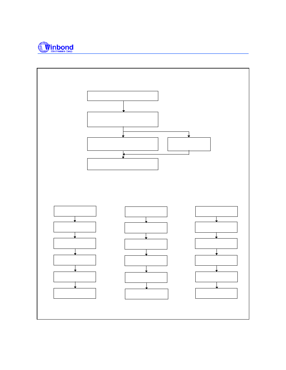
Software Product Identification and Boot Block Lockout Detection Acquisition
Flow
Product
Identification
Entry (1)
Load data 55
to
address 2AAA
Load data 90
to
address 5555
Pause 10 S
Product
Identification
and Boot Block
Lockout Detection
Mode (3)
Read address = 00000
data = DA
Read address = 00001
data = 34
Read address = 7FFF2
Check DQ[3:0] of data
outputs
(4)
Product
Identification Exit(6)
Load data 55
to
address 2AAA
Load data F0
to
address 5555
Normal Mode
(5)
(2)
(2)
Load data AA
to
address 5555
µ
Load data AA
to
address 5555
Pause 10 S
µ
Notes for software product identification/boot block lockout detection:
(1) Data Format: DQ7
- DQ0 (Hex); Address Format: A14 - A0 (Hex)
(2) A1
- A18 = V
IL
; manufacture code is read for A0 = V
IL
; device code is read for A0 = V
IH
.
(3) The device does not remain in identification and boot block lockout detection mode if power down.
(4) The DQ[3:0] to indicate the sectors protect status as below:
DQ0
DQ1
DQ2
DQ3
0
64K Boot Block
Unlocked by Software
16Kbytes Boot Block
Unlocked by Software
64Kbytes Boot Block
Unlocked by #TBL
hardware trapping
Whole Chip Unlocked by #WP
hardware trapping Except Boot
Block
1
64K Boot Block
Locked by Software
16Kbytes Boot Block
Locked by Software
64Kbytes Boot Block
Locked by #TBL hardware
trapping
Whole Chip Locked by #WP
hardware trapping Except Boot
Block
(5) The device returns to standard operation mode.
(6) Optional 1-write cycle (write F0 (hex.) at XXXX address) can be used to exit the product identification/boot block lockout
detection.

W39V040FA
- 14 -
Boot Block Lockout Enable Acquisition Flow
Boot Block Lockout
Feature Set Flow
Load data AA
to
address 5555
Load data 55
to
address 2AAA
Load data 80
to
address 5555
Load data AA
to
address 5555
Load data 55
to
address 2AAA
Load data 40/70
to
address 5555
Exit
40 to lock 64K Boot Block
70 to lcok 16K Boot Block
Pause T
BP

W39V040FA
Publication Release Date: December 19, 2002
- 15 -
Revision A2
7. DC CHARACTERISTICS
Absolute Maximum Ratings
PARAMETER RATING
UNIT
Power Supply Voltage to V
SS
Potential
-0.5 to +4.6
V
Operating Temperature
0 to +70
∞C
Storage Temperature
-65 to +150
∞C
D.C. Voltage on Any Pin to Ground Potential
-0.5 to V
DD
+0.5
V
Transient Voltage (<20 nS) on Any Pin to Ground Potential
-1.0 to V
DD
+0.5
V
Note: Exposure to conditions beyond those listed under Absolute Maximum Ratings May adversely affect the life and reliability
of the device.
Programmer interface Mode DC Operating Characteristics
(V
DD
= 3.3V
±0.3V, V
SS
= 0V, T
A
= 0 to 70
∞ C)
LIMITS
PARAMETER SYM.
TEST
CONDITIONS
MIN. TYP. MAX.
UNIT
Power Supply
Current
I
CC
In Read or Write mode, all DQs open
Address inputs = 3.0V/0V, at f = 3 MHz
- 10 20
mA
Input Leakage
Current
I
LI
V
IN
= V
SS
to V
DD
-
-
90
µA
Output Leakage
Current
I
LO
V
OUT
= V
SS
to V
DD
-
-
90
µA
Input Low Voltage
V
IL
- -0.5
-
0.8
V
Input High Voltage
V
IH
- 2.0
-
V
DD
+0.5
V
Output Low Voltage
V
OL
I
OL
= 2.1 mA
-
-
0.45
V
Output High Voltage V
OH
I
OH
= -0.1mA
2.4
-
-
V

W39V040FA
- 16 -
FWH interface Mode DC Operating Characteristics
(V
DD
= 3.3V
± 0.3V, V
SS
= 0V, T
A
= 0 to 70
∞ C)
LIMITS
PARAMETER SYM. TEST
CONDITIONS
MIN. TYP. MAX.
UNIT
Power Supply Current
I
CC
All I
out
= 0A, CLK = 33 MHz,
in FWH mode operation.
- 12.5 20
mA
Standby Current 1
Isb1
FWH4 = 0.9 V
DD
, CLK = 33 MHz,
all inputs = 0.9 V
DD
/ 0.1 V
DD
no internal operation
- 5 25
uA
Standby Current 2
Isb2
FWH4 = 0.1 V
DD
, CLK = 33 MHz,
all inputs = 0.9 V
DD
/0.1 V
DD
no internal operation.
- 3 10
mA
Input Low Voltage
V
IL
- -0.5
-
0.3
V
DD
V
Input Low Voltage of
#INIT
V
ILI
- -0.5
-
0.2
V
DD
V
Input High Voltage
V
IH
-
0.5
V
DD
- V
DD
+0.5
V
Input High Voltage of
#INIT Pin
V
IHI
- 1.35
V
-
V
DD
+0.5
V
Output Low Voltage
V
OL
I
OL
= 1.5 mA
-
-
0.1 V
DD
V
Output High Voltage
V
OH
I
OH
= -0.5 mA
0.9 V
DD
- - V
Power-up Timing
PARAMETER SYMBOL
TYPICAL
UNIT
Power-up to Read Operation
T
PU
. READ
100
µS
Power-up to Write Operation
T
PU
. WRITE
5
mS
Capacitance
(V
DD
= 3.3V, T
A
= 25
∞ C, f = 1 MHz)
PARAMETER SYMBOL
CONDITIONS
MAX. UNIT
I/O Pin Capacitance
C
I/O
V
I/O
= 0V
12
pF
Input Capacitance
C
IN
V
IN
= 0V
6
pF
W39V040FA
Publication Release Date: December 19, 2002
- 17 -
Revision A2
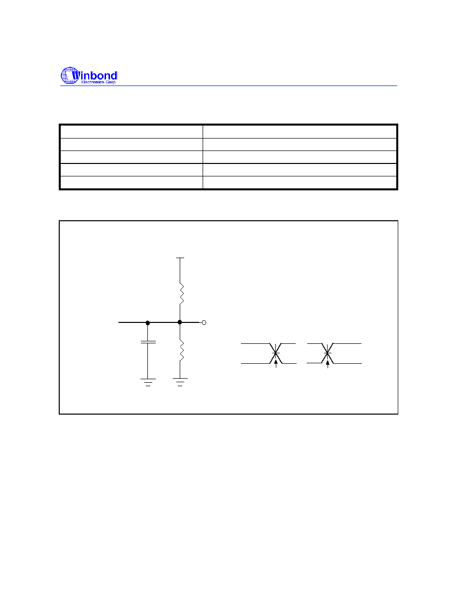
8. PROGRAMMER INTERFACE MODE AC CHARACTERISTICS
AC Test Conditions
PARAMETER CONDITIONS
Input Pulse Levels
0V to 0.9 V
DD
Input Rise/Fall Time
< 5 nS
Input/Output Timing Level
1.5V/1.5V
Output Load
1 TTL Gate and C
L
= 30 pF
AC Test Load and Waveform
+3.3V
1.8K
1.3K
D
OUT
30 pF
(Including Jig and
Scope)
Input
0.9VDD
0V
Test Point
Test Point
1.5V
1.5V
Output

W39V040FA
- 18 -
Programmer Interface Mode AC Characteristics, continued
Read Cycle Timing Parameters
(V
DD
= 3.3V
± 0.3V, V
SS
= 0V, T
A
= 0 to 70
∞ C)
W39V040FA
PARAMETER
SYMBOL
MIN. MAX.
UNIT
Read Cycle Time
T
RC
300 - nS
Row / Column Address Set Up Time
T
AS
50 - nS
Row / Column Address Hold Time
T
AH
50 - nS
Address Access Time
T
AA
- 150
nS
Output Enable Access Time
T
OE
- 75
nS
#OE Low to Active Output
T
OLZ
0 -
nS
#OE High to High-Z Output
T
OHZ
- 35
nS
Output Hold from Address Change
T
OH
0 -
nS
Write Cycle Timing Parameters
PARAMETER SYMBOL
MIN.
TYP.
MAX.
UNIT
Reset Time
T
RST
1 - -
µS
Address Setup Time
T
AS
50 - - nS
Address Hold Time
T
AH
50 - - nS
R/#C to Write Enable High Time
T
CWH
50 - - nS
#WE Pulse Width
T
WP
100 - - nS
#WE High Width
T
WPH
100 - - nS
Data Setup Time
T
DS
50 - - nS
Data Hold Time
T
DH
50 - - nS
#OE Hold Time
T
OEH
0 - - nS
Byte programming Time
T
BP
- 35 50
µS
Sector/Page Erase Cycle Time
T
PEC
- 20 25
mS
Chip Erase Cycle Time
T
EC
- 75
100
mS
Note: All AC timing signals observe the following guidelines for determining setup and hold times:
(a) High level signal's reference level is input high and (b) low level signal's reference level is input low.
Ref. to the AC testing condition.
Data Polling and Toggle Bit Timing Parameters
W39V040FA UNIT
PARAMETER
SYMBOL
MIN. MAX.
#OE to Data Polling Output Delay
T
OEP
- 40
nS
#OE to Toggle Bit Output Delay
T
OET
- 40
nS
W39V040FA
Publication Release Date: December 19, 2002
- 19 -
Revision A2
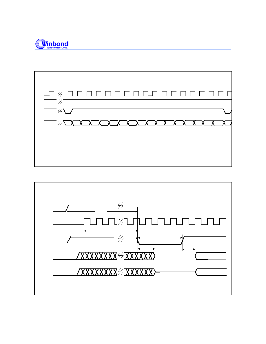
9. TIMING WAVEFORMS FOR PROGRAMMER INTERFACE MODE
Read Cycle Timing Diagram
DQ[7:0]
High-Z
#OE
#WE
V
IH
T
OH
T
AA
Data Valid
T
OHZ
High-Z
T
OLZ
T
OE
#RESET
A[10:0]
T
RC
#C
R/
T
AS
T
AH
Row Address
Column Address
T
AS
T
AH
Column Address
Row Address
T
RST
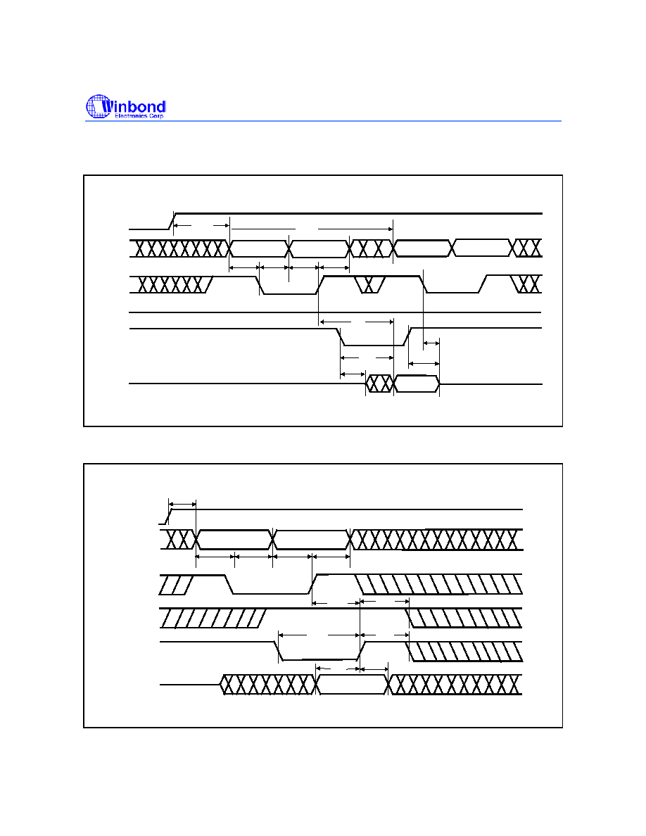
Write Cycle Timing Diagram
Data Valid
T
CWH
T
OEH
T
WP
T
DS
T
AS
T
AH
T
WPH
T
DH
DQ[7:0]
#OE
#WE
#C
R/
#RESET
A[10:0]
Column Address
Row Address
T
RST
T
AS
T
AH
W39V040FA
- 20 -
Timing Waveforms for Programmer Interface Mode, continued
Program Cycle Timing Diagram
A[10:0]
Byte 0
Byte 1
Byte 2
Internal Write Start
DQ[7:0]
#OE
#WE
Byte Program Cycle
T
BP
T
WPH
T
WP
5555
5555
2AAA
AA
A0
55
Programmed Address
Data-In
Byte 3
Note: The internal address A[18:0] are converted from external Column/Row address
Column/Row Address are mapped to the Low/High order internal address.
i.e. Column Address A[10:0] are mapped to the internal A[10:0],
Row Address A[7:0] are mapped to the internal A[18:11].
#C
R/
(Internal A[18:0])
#DATA Polling Timing Diagram
A[10:0]
DQ7
#WE
#OE
X
X
X
T
OEP
T
EC
T
BP or
#C
R/
X
(Internal A[18:0])
An
An
An
An
W39V040FA
Publication Release Date: December 19, 2002
- 21 -
Revision A2
Timing Waveforms for Programmer Interface Mode, continued
Toggle Bit Timing Diagram
A[10:0]
DQ6
#WE
#OE
T
OET
T
EC
T
BP or
#C
R/
Boot Block Lockout Enable Timing Diagram
SB2
SB1
SB0
DQ[7:0]
#OE
#WE
SB3
SB4
SB5
T
WP
T
WPH
AA
55
80
40/70
AA
55
Note: The internal address A[18:0] are converted from external Column/Row add
Column/Row Address are mapped to the Low/High order internal addr
i.e. Column Address A[10:0] are mapped to the internal A[10:
Row Address A[7:0] are mapped to the internal A[18:11
(Internal A[18:0])
Six-byte code for Boot Block Lockout command
5555
2AAA
5555
5555
2AAA
5555
A[10:0]
#C
R/
T
WC
When 40(hex) is loaded, the 64KByte are locked; while 70(hex) is loaded, the 16KByte is lo
W39V040FA
- 22 -
Timing Waveforms for Programmer Interface Mode, continued
Chip Erase Timing Diagram
DQ[7:0]
AA
55
80
AA
55
10
SB2
SB1
SB0
#OE
#WE
SB3
SB4
SB5
Internal Erasure Starts
T
WP
T
WPH
T
EC
#C
R/
Note: The internal address A[18:0] are converted from external Column/Row addre
Column/Row Address are mapped to the Low/High order internal addre
i.e. Column Address A[10:0] are mapped to the internal A[10:0],
Row Address A[7:0] are mapped to the internal A[18:11].
(Internal A[18:0])
Six-byte code for 3.3V-only software chip erase
5555
2AAA
5555
5555
2AAA
5555
A[10:0]
Sector/Page Erase Timing Diagram
SB2
SB1
SB0
A[10:0]
DQ[7:0]
#OE
#WE
SB3
SB4
SB5
Internal Erase starts
Six-byte code for 3.3V-only
Sector/Page Erase
T
WP
T
WPH
T
PEC
5555
2AAA
5555
5555
2AAA
SA/PA
AA
55
80
AA
55
30/50
SA = Sector Address and PA = Page Address, Please ref. to the "Table of Command Definition"
Note: The internal address A[18:0] are converted from external Column/Row address
Column/Row Address are mapped to the Low/High order internal address
i.e. Column Address A[10:0] are mapped to the internal A[10:0],
Row Address A[7:0] are mapped to the internal A[18:11].
#C
R/
(Internal A[18:0])
W39V040FA
Publication Release Date: December 19, 2002
- 23 -
Revision A2
10. FWH INTERFACE MODE AC CHARACTERISTICS
AC Test Conditions
PARAMETER CONDITIONS
Input Pulse Levels
0.6 V
DD
to 0.2 V
DD
Input Rise/Fall Slew Rate
1 V/nS
Input/Output Timing Level
0.4V
DD
/ 0.4V
DD
Output Load
1 TTL Gate and C
L
= 10 pF
Read/Write Cycle Timing Parameters
(V
DD
= 3.3V
± 0.3V, V
SS
= 0V, T
A
= 0 to 70
∞ C)
W39V040FA
PARAMETER
SYMBOL
MIN. MAX.
UNIT
Clock Cycle Time
T
CYC
30 - nS
Input Set Up Time
T
SU
7 -
nS
Input Hold Time
T
HD
0 -
nS
Clock to Data Valid
T
KQ
2 11
nS
Note: Minimum and Maximum time has different loads. Please refer to PCI specification.
Reset Timing Parameters
PARAMETER SYMBOL
MIN.
TYP.
MAX.
UNIT
V
DD
stable to Reset Active
T
PRST
1 - -
mS
Clock Stable to Reset Active
T
KRST
100 - -
µS
Reset Pulse Width
T
RSTP
100 - - nS
Reset Active to Output Float
T
RSTF
- - 50
nS
Reset Inactive to Input Active
T
RST
10 - -
µS
Note: All AC timing signals observe the following guidelines for determining setup and hold times:
(a) High level signal's reference level is input high and (b) low level signal's reference level is input low.
Ref. to the AC testing condition.
W39V040FA
- 24 -
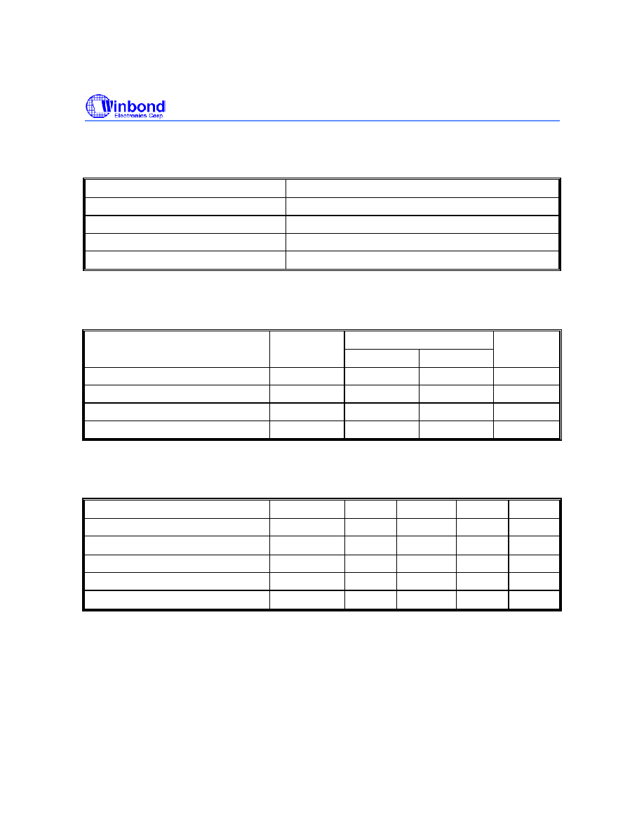
11. TIMING WAVEFORMS FOR FWH INTERFACE MODE
Read Cycle Timing Diagram
T
CYC
FWH4
#RESET
FWH[3:0]
Start
FWH
Read
IDSEL
CLK
1 Clock
2 Clocks
A[15:12]
Address
Sync
TAR
1111b
Tri-State
0000b
T
KQ
T
HD
T
SU
A[11:8]
A[7:4]
0000
b]
Data out 2 Clocks
D[7:4]
Data
D[3:0]
Next Start
1 Clock
0000b
T
HD
T
SU
Load Address in 7
Clocks
A[3:0]
M Size
XXXXb
XA[22]XXb XXA[18:16]
1 Clock
1 Clock
0000b
1101b
Note: When A22 = high, the host will read the BIOS code from the FWH d
While A22 = low, the host will read the GPI (Add = FFBC0100
Product ID (Add = FFBC0000/FFBC0001) from the FWH dev
1111b
Tri-State
2 Clocks
TAR
Write Cycle Timing Diagram
TCYC
FWH4
#RESET
FWH[3:0]
Start
FWH
Write
IDSEL
CLK
Next Start
1 Clock
1 Clock
A[15:12]
Load Data in 2 Clocks
D[7:4]
Address
Sync
2 Clocks
TAR
Data
1111b
Tri-State
0000b
THD
TSU
A[11:8]
A[7:4]
0000b
D[3:0]
0000b
Load Address in 7 Clocks
A[3:0]
M Size
XXXXb
XXXXb
XXA[18:16]b
1 Clock
1 Clock
0000b
1110b
2 Clocks
TAR
1111b
Tri-State

W39V040FA
Publication Release Date: December 19, 2002
- 25 -
Revision A2
Timing Waveforms, for FWH Interface Mode, continued
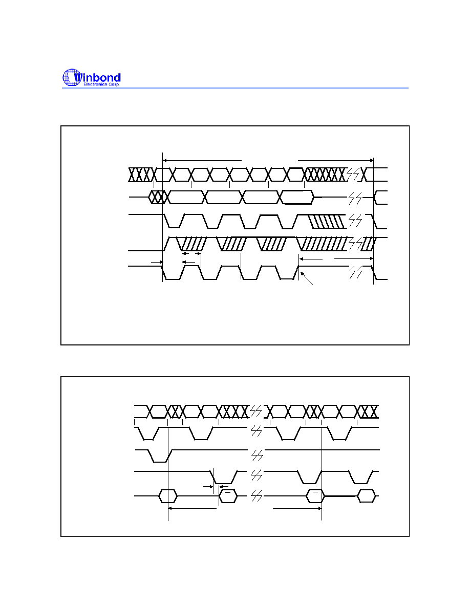
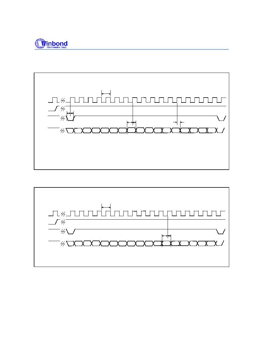
Program Cycle Timing Diagram
FWH4
#RESET
FWH[3:0 ]
1st Start
IDSEL
Load Address "5555" in 7 Clocks
CLK
1 Clock
2 Clocks
Load Data "AA" in 2 Clocks
1010b
1010b
Write the 1st command to the device in FWH mode.
2nd Start
Load Address "2AAA" in 7 Clocks
1 Clock
2 Clocks
Load Data "55"
in 2 Clocks
0101b
0101b
Write the 2nd command to the device in FWH mode.
3rd Start
Load Address "5555" in 7 Clocks
1 Clock
2 Clocks
Load Data "A0"
in 2 Clocks
1010b
0000b
Write the 3rd command to the device in FWH mode.
4th Start
Load Ain in 7 Clocks
FWH4
#RESET
FWH[3:0 ]
CLK
FWH4
#RESET
FWH[3:0 ]
CLK
FWH4
#RESET
FWH[3:0 ]
CLK
Sync
Internal
program start
TAR
1 Clock
2 Clocks
A[15:12]
Load Din in 2 Clocks
D[7:4]
Write the 4th command(target location to be programmed) to the device in FWH mode.
A[11:8]
A[7:4]
A[3:0]
D[3:0]
1111b
Tri-State
0000b
Data
Address
Address
Address
Address
Sync
TAR
Data
Sync
TAR
Data
Sync
TAR
Data
1111b
Tri-State
0000b
1111b
Tri-State
0000b
1111b
Tri-State
0000b
IDSEL
Internal
program start
IDSEL
IDSEL
0000b
0000b
0000b
0000b
X101b
0101b
0101b
0101b
X010b
1010b
1010b
1010b
X101b
0101b
0101b
0101b
M Size
M Size
M Size
M Size
XXXXb
XXXXb
XXXXb
XXXXb
XXXXb
XXXXb
XXXXb
XA[18:16]b
XXXXb
XXXXb
XXXXb
XXXXb
1 Clock
1 Clock
0000b
1110b
1 Clock
1 Clock
0000b
1110b
1 Clock
1 Clock
0000b
1110b
1 Clock
1 Clock
0000b
1110b
Start next
command
1 Clock
2 Clocks
TAR
1111b
Tri-State
Start next
command
1 Clock
2 Clocks
TAR
1111b
Tri-State
Start next
command
1 Clock
2 Clocks
TAR
1111b
Tri-State
TAR
2 Clocks
1111b Tri-State
W39V040FA
- 26 -
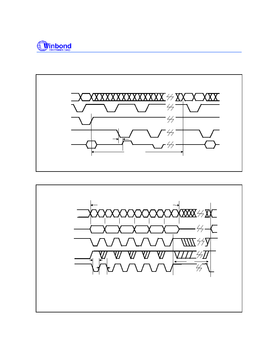
Timing Waveforms for FWH Interface Mode, continued
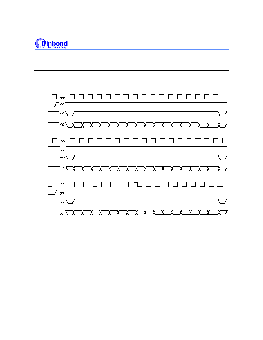
#DATA Polling Timing Diagram
Read the DQ7 to see if the internal write complete or not.
FWH4
#RESET
FWH[3:0]
Start
Load Address in 7 Clocks
CLK
1 Clock
2 Clocks
XXXXb
An[15:12]
Address
Sync
TAR
1111b
Tri-State
0000b
An[11:8]
An[7:4]
An[3:0]
Data out 2 Clocks
Dn7,xxx
Data
XXXXb
FWH4
#RESET
FWH[3:0]
Start
Load Address in 7 Clocks
CLK
1 Clock
2 Clocks
Address
Sync
TAR
1111b
Tri-State
0000b
Data out 2 Clocks
Data
When internal write complete, the DQ7 will equal to Dn7.
Dn7,xxx
XXXXb
An[15:12]
An[11:8]
An[7:4]
An[3:0]
FWH4
#RESET
FWH[3:0]
Start
Load Address "An" in 7 Clocks
CLK
1 Clock
2 Clocks
An[15:12]
Load Data "Dn"
in 2 Clocks
Dn[7:4]
Write the last command(program or erase) to the device in FWH mode.
Address
Sync
TAR
Data
1111b
Tri-State
0000b
An[11:8]
An[7:4]
An[3:0]
Dn[3:0]
IDSEL
IDSEL
IDSEL
0000b
0000b
0000b
M Size
M Size
M Size
XXXXb
XXA[18:16]b
XXXXb
XXXXb
XXA[18:16]b
XXXXb
XXXXb
XXA[18:16]b
XXXXb
1 Clock
2 Clocks
TAR
1111b
Tri-State
Next Start
1 Clock
2 Clocks
TAR
1111b
Tri-State
Next Start
1 Clock
2 Clocks
TAR
1111b
Tri-State
Next Start
1 Clock
1 Clock
0000b
1101b
1 Clock
1 Clock
0000b
1101b
1 Clock
1 Clock
0000b
1110b
W39V040FA
Publication Release Date: December 19, 2002
- 27 -
Revision A2
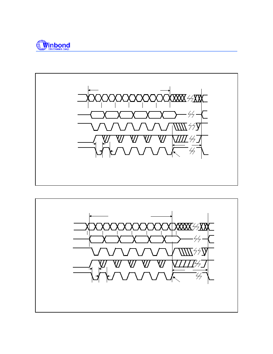
Timing Waveforms for FWH Interface Mode, continued
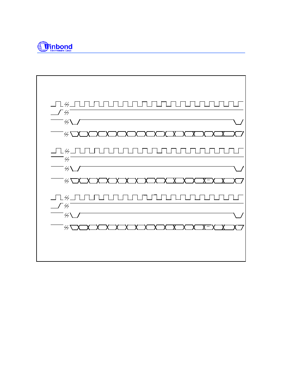
Toggle Bit Timing Diagram
Read the DQ6 to see if the internal write complete or not.
FWH4
#RESET
Start
Load Address in 7 Clocks
CLK
1 Clock
2 Clocks
Address
Sync
TAR
1111b
Tri-State
0000b
Data out 2 Clocks
X,D6,XXb
Data
XXXXb
FWH4
#RESET
FWH[3:0]
Start
Load Address in 7 Clocks
CLK
1 Clock
2 Clocks
Address
Sync
TAR
1111b
Tri-State
0000b
Data out 2 Clocks
Data
When internal write complete, the DQ6 will stop toggle.
X,D6,XXb
XXXXb
FWH4
#RESET
FWH[3:0]
Start
Load Address "An" in 7 Clocks
CLK
1 Clock
2 Clocks
A[15:12]
Load Data "Dn"
in 2 Clocks
D[7:4]
Write the last command(program or erase) to the device in FWH mode.
Address
Sync
TAR
Data
1111b
Tri-State
0000b
A[11:8]
A[7:4]
A[3:0]
D[3:0]
IDSEL
XXXXb
XXXXb
XXXXb
XXXXb
XXXXb
XXXXb
XXXXb
XXXXb
IDSEL
IDSEL
0000b
0000b
0000b
M Size
M Size
M Size
XXXXb
XXXXb
XXXXb
XXXXb
XXXXb
XXA[18:16]b
XXXXb
XXXXb
XXXXb
1 Clock
1 Clock
0000b
1110b
1 Clock
1 Clock
0000b
1101b
1 Clock
1 Clock
0000b
1101b
1 Clock
2 Clocks
TAR
1111b
Tri-State
Next Start
1 Clock
2 Clocks
TAR
1111b
Tri-State
Next Start
1 Clock
2 Clocks
TAR
1111b
Tri-State
Next Start
FWH[3:0]

W39V040FA
- 28 -
Timing Waveforms for FWH Interface Mode, continued
Boot Block Lockout Enable Timing Diagram
CLK
#RESET
FWH4
FWH[3:0]
1st Start
Load Address "5555" in 7 Clocks
1 Clock
2 Clocks
X101b
0101b
0101b
0101b
Load Data "AA"
in 2 Clocks
1010b
1010b
Write the 1st command to the device in FWH mode.
Address
Sync
TAR
Data
1111b
Tri-State
0000b
IDSEL
0000b
M Size
XXXXb
XXXXb
XXXXb
Start next
command
1 Clock
2 Clocks
TAR
1111b
Tri-State
1 Clock
1 Clock
0000b
1110b
CLK
#RESET
2nd Start
Load Address "2AAA" in 7 Clocks
1 Clocks
2 Clocks
X010b
1010b
1010b
1010b
Load Data "55"
in 2 Clocks
0101b
0101b
Write the 2nd command to the device in FWH mode.
Address
Sync
TAR
Data
1111b
Tri-State
0000b
IDSEL
0000b
M Size
XXXXb
XXXXb
XXXXb
Start next
command
1 Clock
2 Clocks
TAR
1111b
Tri-State
1 Clock
1 Clock
0000b
1110b
FWH4
FWH[3:0]
CLK
#RESET
3rd Start
Load Address "5555" in 7 Clocks
1 Clock
2 Clocks
X101b
0101b
0101b
0101b
Load Data "80"
in 2 Clocks
1000b
0000b
Write the 3rd command to the device in FWH mode.
Address
Sync
TAR
Data
1111b
Tri-State
0000b
IDSEL
0000b
M Size
XXXXb
XXXXb
XXXXb
Start next
command
1 Clock
2 Clocks
TAR
1111b
Tri-State
1 Clock
1 Clock
0000b
1110b
FWH4
FWH[3:0]
CLK
#RESET
4th Start
Load Address "5555" in 7 Clocks
1 Clock
2 Clocks
X101b
0101b
0101b
0101b
Load Data "AA"
in 2 Clocks
1010b
1010b
Write the 4th command to the device in FWH mode.
Address
Sync
TAR
Data
1111b
Tri-State
0000b
IDSEL
0000b
M Size
XXXXb
XXXXb
XXXXb
Start next
command
1 Clock
2 Clocks
TAR
1111b
Tri-State
1 Clock
1 Clock
0000b
1110b
FWH4
FWH[3:0]
CLK
#RESET
5th Start
Load Address "2AAA" in 7 Clocks
1 Clock
2 Clocks
X010b
1010b
1010b
1010b
Load Data "55"
in 2 Clocks
0101b
0101b
Write the 5th command to the device in FWH mode.
Address
Sync
TAR
Data
1111b
Tri-State
0000b
IDSEL
0000b
M Size
XXXXb
XXXXb
XXXXb
Start next
command
1 Clock
2 Clocks
TAR
1111b
Tri-State
1 Clock
1 Clock
0000b
1110b
FWH4
FWH[3:0]
CLK
#RESET
6th Start
Load Address "5555" 7 Clocks
Sync
TAR
1 Clock
2 Clocks
X101b
Load Data "40" or
"70" in Two Clocks
0100b/
0111b
Write the 6th command to the device in FWH mode.
0101b
0101b
0101b
0000b
1111b
Tri-State
0000b
Data
Address
IDSEL
0000b
M Size
XXXXb
XXXXb
XXXXb
1 Clock
1 Clock
0000b
1110b
FWH4
FWH[3:0]
Start next
command
1 Clock
2 Clocks
TAR
1111b
Tri-State
W39V040FA
Publication Release Date: December 19, 2002
- 29 -
Revision A2
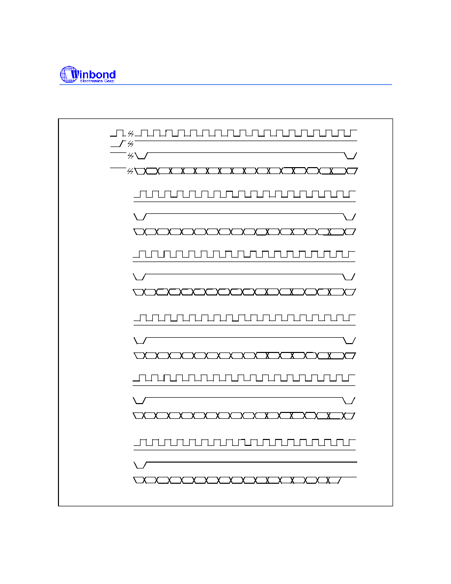
Timing Waveforms for FWH Interface Mode, continued
Chip Erase Timing Diagram
Load Address "5555" in 7 Clocks
Sync
Internal
erase start
TAR
1 Clock
X101b
Load Data "10"
in 2 Clocks
0001b
Write the 6th command to the device in FWH mode.
0101b
0101b
0101b
0000b
1111b
Tri-State
0000b
Data
Address
FWH4
#RESET
FWH[3:0]
1st Start
CLK
X101b
0101b
0101b
0101b
1010b
1010b
FWH4
#RESET
FWH[3:0]
CLK
FWH4
#RESET
FWH[3:0]
CLK
FWH4
#RESET
FWH[3:0]
CLK
Address
Sync
TAR
Data
Load Address "5555" in 7 Clocks
1 Clock
2 Clocks
Load Data "AA"
in 2 Clocks
Write the 1st command to the device in FWH mode.
Load Address "2AAA" in 7 Clocks
1 Clock
2 Clocks
X010b
1010b
1010b
1010b
Load Data "55"
in 2 Clocks
0101b
0101b
Write the 2nd command to the device in FWH mode.
Load Address "5555" in 7 Clocks
1 Clock
2 Clocks
X101b
0101b
0101b
0101b
Load Data "80"
in 2 Clocks
1000b
0000b
Write the 3rd command to the device in FWH mode.
Address
Address
Sync
TAR
Data
Sync
TAR
Data
1111b
Tri-State
0000b
1111b
Tri-State
0000b
1111b
Tri-State
0000b
Load Address "5555" in 7 Clocks
1 Clock
2 Clocks
X101b
0101b
0101b
0101b
Load Data "AA"
in 2 Clocks
1010b
1010b
Write the 4th command to the device in FWH mode.
Load Address "2AAA" in 7 Clocks
1 Clock
2 Clocks
X010b
1010b
1010b
1010b
Load Data "55"
in 2 Clocks
0101b
0101b
Write the 5th command to the device in FWH mode.
Address
Address
Sync
TAR
Data
Sync
TAR
Data
1111b
Tri-State
0000b
1111b
Tri-State
0000b
FWH4
#RESET
FWH[3:0]
CLK
FWH4
#RESET
FWH[3:0]
CLK
2 Clocks
IDSEL
0000b
0000b
0000b
0000b
0000b
0000b
M Size
M Size
M Size
M Size
M Size
M Size
XXXXb
XXXXb
XXXXb
XXXXb
XXXXb
XXXXb
XXXXb
XXXXb
XXXXb
XXXXb
XXXXb
XXXXb
XXXXb
XXXXb
XXXXb
XXXXb
XXXXb
XXXXb
Start next
command
1 Clock
2 Clocks
TAR
1111b
Tri-State
Start next
command
1 Clock
2 Clocks
TAR
1111b
Tri-State
Start next
command
1 Clock
2 Clocks
TAR
1111b
Tri-State
Start next
command
1 Clock
2 Clocks
TAR
1111b
Tri-State
Start next
command
1 Clock
2 Clocks
TAR
1111b
Tri-State
Internal
erase start
TAR
2 Clocks
1111b Tri-State
6th Start
IDSEL
5th Start
IDSEL
4th Start
IDSEL
3th Start
IDSEL
2th Start
IDSEL
1 Clock
1 Clock
0000b
1110b
1 Clock
1 Clock
0000b
1110b
1 Clock
1 Clock
0000b
1110b
1 Clock
1 Clock
0000b
1110b
1 Clock
1 Clock
0000b
1110b
1 Clock
1 Clock
0000b
1110b

W39V040FA
- 30 -
Timing Waveforms for FWH Interface Mode, continued
Sector Erase Timing Diagram
6th Start
Load Sector Address in 7 Clocks
Sync
Internal
erase start
1 Clock
Load Din
in 2 Clocks
0011b
Write the 6th command(target sector to be erased) to the device in FWH mode.
0000b
TAR
2 Clocks
1111b
Tri-State
0000b
Data
Address
#RESET
1st Start
Load Address "5555" in 7 Clocks
CLK
1 Clock
1 Clock
Start next
command
1 Clock
2 Clocks
1 Clock
X101b
0101b
0101b
0101b
Load Data "AA"
in 2 Clocks
1010b
1010b
Write the 1st command to the device in FWH mode.
FWH4
#RESET
FWH[3:0]
CLK
FWH4
#RESET
FWH[3:0]
CLK
FWH4
#RESET
CLK
Address
Sync
TAR
Data
2nd Start
Load Address "2AAA" in 7 Clocks
1 Clock
1 Clock
Start next
command
1 Clock
2 Clocks
1 Clock
X010b
1010b
1010b
1010b
Load Data "55"
in 2 Clocks
0101b
0101b
Write the 2nd command to the device in FWH mode.
3rd Start
Load Address "5555" in 7 Clocks
1 Clocks
1 Clocks
Start next
command
1 Clocks
2 Clocks
1 Clocks
X101b
0101b
0101b
0101b
Load Data "80"
in 2 Clocks
1000b
0000b
Write the 3rd command to the device in FWH mode.
Address
Address
Sync
TAR
Data
Sync
TAR
Data
1111b
Tri-State
0000b
1111b
Tri-State
0000b
1111b
Tri-State
0000b
4th Start
Load Address "5555" in 7 Clocks
1 Clock
1 Clock
Start next
command
1 Clock
2 Clocks
1 Clock
X101b
0101b
0101b
0101b
Load Data "AA"
in 2 Clocks
1010b
1010b
Write the 4th command to the device in FWH mode.
5th Start
Load Address "2AAA" in 7 Clocks
1 Clock
1 Clock
Start next
command
1 Clock
1 Clock
X010b
1010b
1010b
1010b
Load Data "55"
in 2 Clocks
0101b
0101b
Write the 5th command to the device in FWH mode.
Address
Address
Sync
2 Clocks
TAR
Data
Sync
TAR
Data
1111b
Tri-State
0000b
1111b
Tri-State
0000b
FWH4
#RESET
FWH[3:0]
CLK
FWH4
#RESET
FWH[3:0]
CLK
XXXXb
XXXXb
XXXXb
IDSEL
Internal
erase start
0000b
1110b
IDSEL
0000b
1110b
IDSEL
0000b
1110b
IDSEL
0000b
1110b
IDSEL
0000b
1110b
IDSEL
0000b
0000b
0000b
0000b
0000b
0000b
M Size
M
Size
M Size
M Size
M Size
M Size
XXXXb
XXXXb
XXXXb
XXXXb
XXXXb
XXXXb
XXXXb
XXXXb
XXXXb
XXXXb
XXXXb
XA[18:16]b
XXXXb
XXXXb
XXXXb
XXXXb
XXXXb
XXXXb
TAR
2 Clocks
1111b Tri-State
2 Clocks
TAR
1111b
Tri-State
2 Clocks
TAR
1111b
Tri-State
2 Clocks
TAR
1111b
Tri-State
2 Clocks
TAR
1111b
Tri-State
2 Clocks
TAR
1111b
Tri-State
1 Clock
1 Clock
0000b
1110b
FWH[3:0]
FWH4
FWH[3:0]
XXXXb

W39V040FA
Publication Release Date: December 19, 2002
- 31 -
Revision A2
Timing Waveforms for FWH Interface Mode, continued
Page Erase Timing Diagram
CLK
#RESET
FWH4
1st Start
Load Address "5555" in 7 Clocks
1 Clock
1 Clock
Start next
command
1 Clock
2 Clocks
1 Clock
X101b
0101b
0101b
0101b
Load Data "AA"
in 2 Clocks
1010b
1010b
Write the 1st command to the device in FWH mode.
Address
Sync
TAR
Data
1111b
Tri-State
0000b
0000b
1110b
IDSEL
0000b
M Size
XXXXb
XXXXb
XXXXb
2 Clocks
TAR
1111b
Tri-State
#RESET
CLK
FWH4
FWH[3:0]
#RESET
CLK
2nd Start
Load Address "2AAA" in 7 Clocks
1 Clock
1 Clock
Start next
command
1 Clock
2 Clocks
1 Clock
X010b
1010b
1010b
1010b
Load Data "55"
in 2 Clocks
0101b
0101b
Write the 2nd command to the device in FWH mode.
Address
Sync
TAR
Data
1111b
Tri-State
0000b
0000b
1110b
IDSEL
0000b
M
Size
XXXXb
XXXXb
XXXXb
2 Clocks
TAR
1111b
Tri-State
FWH4
FWH[3:0]
#RESET
CLK
3rd Start
Load Address "5555" in 7 Clocks
1 Clocks
1 Clocks
Start next
command
1 Clocks
2 Clocks
1 Clocks
X101b
0101b
0101b
0101b
Load Data "80"
in 2 Clocks
1000b
0000b
Write the 3rd command to the device in FWH mode.
Address
Sync
TAR
Data
1111b
Tri-State
0000b
0000b
1110b
IDSEL
0000b
M Size
XXXXb
XXXXb
XXXXb
2 Clocks
TAR
1111b
Tri-State
FWH4
4th Start
Load Address "5555" in 7 Clocks
1 Clock
1 Clock
Start next
command
1 Clock
2 Clocks
1 Clock
X101b
0101b
0101b
0101b
Load Data "AA"
in 2 Clocks
1010b
1010b
Write the 4th command to the device in FWH mode.
Address
Sync
TAR
Data
1111b
Tri-State
0000b
#RESET
CLK
0000b
1110b
IDSEL
0000b
M Size
XXXXb
XXXXb
XXXXb
2 Clocks
TAR
1111b
Tri-State
5th Start
Load Address "2AAA" in 7 Clocks
1 Clock
1 Clock
Start next
command
1 Clock
1 Clock
X010b
1010b
1010b
1010b
Load Data "55"
in 2 Clocks
0101b
0101b
Write the 5th command to the device in FWH mode.
Address
Sync
2 Clocks
TAR
Data
1111b
Tri-State
0000b
FWH4
FWH[3:0]
0000b
1110b
IDSEL
0000b
M Size
XXXXb
XXXXb
XXXXb
2 Clocks
TAR
1111b
Tri-State
#RESET
CLK
6th Start
Load Page Address in 7 Clocks
Sync
Internal
erase start
1 Clock
A[15:12]
Load Din
in 2 Clocks
0101b
Write the 6th command(target page to be erased) to the device in FWH mode.
0000b
TAR
2 Clocks
1111b
Tri-State
0000b
Data
Address
FWH4
FWH[3:0]
XXXXb
XXXXb
XXXXb
IDSEL
Internal
erase start
0000b
M Size
XXXXb
XA[18:16]b
XXXXb
TAR
2 Clocks
1111b Tri-State
1 Clock
1 Clock
0000b
1110b
FWH[3:0]
FWH[3:0]
W39V040FA
- 32 -
Timing Waveforms for FWH Interface Mode, continued
FGPI Register/Product ID Readout Timing Diagram
Note: During the GPI read out mode, the DQ[4:0] will capture the states(High or Low) of the FGPI[4:0] input pins. The DQ[7:5] are reserved pins
#RESET
FWH[3:0]
Start
IDSEL
Load Address "FFBC0100(hex)" in 7 Clocks for GPI Register
& "FFBC0000(hex)/FFBC0001(hex) for Product ID
CLK
1 Clock
1 Clock
Next Sta
1 Clock
2 Clocks
1 Clock
0000b
1101b
Address
Sync
TAR
1111b
Tri-State
0000b
Data out 2 Clocks
D[7:4]
Data
0000b
0001b
/0000b
0000b
0000b
/0001b
D[3:0]
A[27:24]
A[23:20] A[19:16]
0000b
M Size
2 Clocks
TAR
1111b
Tri-State
FWH4
Reset Timing Diagram
CLK
VDD
#RESET
FWH[3:0]
T
PRST
T
KRST
T
RSTP
T
RST
F
T
RST
FWH4
W39V040FA
Publication Release Date: December 19, 2002
- 33 -
Revision A2
12. ORDERING INFORMATION
PART NO.
ACCESS
TIME
(nS)
POWER SUPPLY
CURRENT MAX.
(mA)
STANDBY VDD
CURRENT MAX.
(mA)
PACKAGE
W39V040FAP 11
20
10 32L
PLCC
W39V040FAQ 11
20
10 32L
STSOP
W39V040FAT 11
20
10 40L
TSOP
Notes:
1. Winbond reserves the right to make changes to its products without prior notice.
2. Purchasers are responsible for performing appropriate quality assurance testing on products intended for use in
applications where personal injury might occur as a consequence of product failure.
13. HOW TO READ THE TOP MARKING
Example: The top marking of 32-pin STSOP W39V040FAQ
1
st
line: Winbond logo
2
nd
line: the part number: W39V040FAQ
3
rd
line: the lot number
4
th
line: the tracking code: 149 O B SA
149: Packages made in '01, week 49
O: Assembly house ID: A means ASE, O means OSE, ...etc.
B: IC revision; A means version A, B means version B, ...etc.
SA: Process code
W39V040FAQ
2138977A-A12
149OBSA
W39V040FA
- 34 -
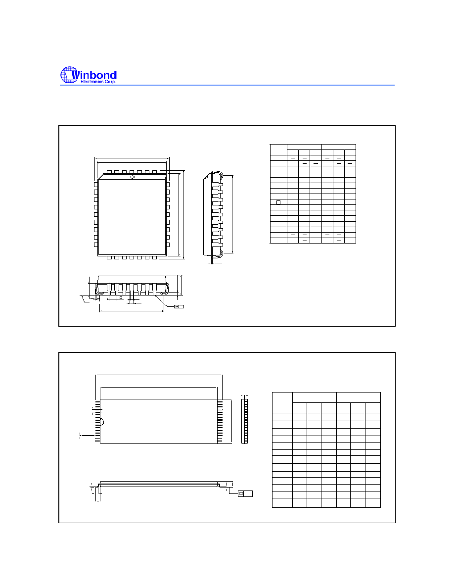
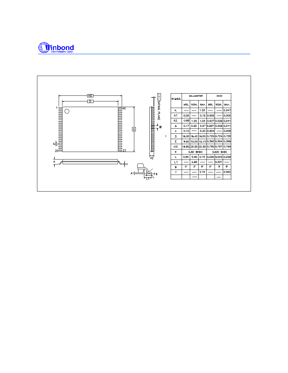
14. PACKAGE DIMENSIONS
32L PLCC
Notes:
L
c
1
b
2
A
H
E
E
e
b
D H
D
y
A
A
1
Seating Plane
E
G
G
D
1
13
14
20
29
32
4
5
21
30
1. Dimensions D & E do not include interlead flash.
2. Dimension b1 does not include dambar protrusion/intrusio
3. Controlling dimension: Inches
4. General appearance spec. should be based on final
visual inspection sepc.
Symbol
Min. Nom. Max.
Max.
Nom.
Min.
Dimension in Inches
Dimension in mm
A
b
c
D
e
H
E
L
y
A
A
1
2
E
b
1
G
D
3.56
0.50
2.80
2.67
2.93
0.71
0.66
0.81
0.41
0.46
0.56
0.20
0.25
0.35
13.89
13.97
14.05
11.35
11.43
11.51
1.27
H
D
G
E
12.45
12.95
13.46
9.91
10.41
10.92
14.86
14.99
15.11
12.32
12.45
12.57
1.91
2.29
0.004
0.095
0.090
0.075
0.495
0.490
0.485
0.595
0.590
0.585
0.430
0.410
0.390
0.530
0.510
0.490
0.050
0.453
0.450
0.447
0.553
0.550
0.547
0.014
0.010
0.008
0.022
0.018
0.016
0.032
0.026
0.028
0.115
0.105
0.110
0.020
0.140
1.12
1.42
0.044
0.056
0
10
10
0
0.10
2.41
32L STSOP
Min.
Dimension in Inches
Nom. Max. Min. Nom. Max.
Symbol
1.20
0.05
0.15
1.05
1.00
0.95
0.17
0.10
0.50
0.00
0
0.22
0.27
-----
0.21
12.40
8.00
14.00
0.50
0.60
0.70
0.80
0.10
3
5
0.047
0.006
0.041
0.040
0.035
0.007
0.009
0.010
0.004
-----
0.008
0.488
0.315
0.551
0.020
0.020
0.024
0.028
0.031
0.000
0.004
0
3
5
0.002
A
A
b
c
D
E
e
L
L
Y
1
1
2
A
H
D
Dimension in mm
A
A
A
2
1
L
L
1
Y
E
H
D
D
c
b
e
W39V040FA
Publication Release Date: December 19, 2002
- 35 -
Revision A2
Package Dimensions, continued
40L TSOP (10 mm x 20 mm)
R
R
0.08
0.008
0.003
0.02
W39V040FA
- 36 -
15. VERSION HISTORY
VERSION DATE PAGE
DESCRIPTION
A1
June 19, 2002
-
Initial Issued
A2
Dec. 19, 2002
23
Delete AC Test Load and Waveform.
Add a note below Read/Write Cycle Timing
Parameter
15
Modify PGM mode power supply current (Icc)
parameter from 20 mA (typ.) to 10 mA (typ.) and
30 mA (max.) to 20 mA (max.)
1, 16, 33
Modify FWH mode power supply current (Icc)
parameter from 40 mA (typ.) to 12.5 mA (typ.) and
60 mA (max.) to 20 mA (max.)
16
Modify Standby current (Isb1) parameter from 20
µA
(typ.) to 5
µA (typ.) and 100 µA (max.) to 25 µA
(max.)
Headquarters
No. 4, Creation Rd. III,
Science-Based Industrial Park,
Hsinchu, Taiwan
TEL: 886-3-5770066
FAX: 886-3-5665577
http://www.winbond.com.tw/
Taipei Office
TEL: 886-2-8177-7168
FAX: 886-2-8751-3579
Winbond Electronics Corporation America
2727 North First Street, San Jose,
CA 95134, U.S.A.
TEL: 1-408-9436666
FAX: 1-408-5441798
Winbond Electronics (H.K.) Ltd.
No. 378 Kwun Tong Rd.,
Kowloon, Hong Kong
FAX: 852-27552064
Unit 9-15, 22F, Millennium City,
TEL: 852-27513100
Please note that all data and specifications are subject to change without notice.
All the trade marks of products and companies mentioned in this data sheet belong to their respective owners.
Winbond Electronics (Shanghai) Ltd.
200336 China
FAX: 86-21-62365998
27F, 2299 Yan An W. Rd. Shanghai,
TEL: 86-21-62365999
Winbond Electronics Corporation Japan
Shinyokohama Kohoku-ku,
Yokohama, 222-0033
FAX: 81-45-4781800
7F Daini-ueno BLDG, 3-7-18
TEL: 81-45-4781881
9F, No.480, Rueiguang Rd.,
Neihu District, Taipei, 114,
Taiwan, R.O.C.