 | –≠–ª–µ–∫—Ç—Ä–æ–Ω–Ω—ã–π –∫–æ–º–ø–æ–Ω–µ–Ω—Ç: W45B512 | –°–∫–∞—á–∞—Ç—å:  PDF PDF  ZIP ZIP |

Preliminary W45B512
512K
◊
1 SERIAL FLASH
Publication Release Date: February 21, 2002
- 1 - Revision A1
GENERAL DESCRIPTION
The W45B512 is manufactured with Winbond's high performance CMOS WinFlash technology. The
Serial Flash is organized as 16 sectors of 4096 Bytes for the W45B512. The memory is accessed for
Read or Erase/Program by the SPI bus compatible serial protocol. The bus signals are: serial data
input (SI), serial data output (SO), serial clock (SCK), write protect (#WP), chip enable (#CE), and
hardware reset (#RESET). This device is offered in 8L SON and 32L PLCC package.
FEATURES
∑
Single 2.7
-
3.6V Read and Write Operations
∑
Serial Interface Architecture
-
SPI Compatible: Mode 0 and Mode 3
∑
Byte Serial Read with Single Command
∑
Superior Reliability
-
Endurance: 10,000 Cycles (Typ.)
-
20 years Data Retention
∑
Low Power Consumption
-
Active Current: 30 mA (Max.)
-
Standby Current: 15 µA (Max.)
∑
Sector or Chip-erase Capability
-
Uniform 4 KByte sectors
∑
Fast Erase and Byte-program
-
Chip-erase Time: 100 mS (Max.)
-
Sector-erase Time: 25 mS (Max.)
-
Byte-program Time: 50 µS (Max.)
∑
Automatic Write Timing
-
Internal V
PP
Generation
∑
End-of-Write Detection
-
Software Status
∑
20 MHz Max Clock Frequency
∑
Hardware Reset Pin (#RESET)
-
Resets the device to Standby Mode
∑
TTL Compatibility
∑
Hardware Data Protection
-
Protects/Unprotects the device from Write
operation
∑
Packages Available
8L SON (5 x 6 mm), 32L PLCC
Preliminary W45B512
- 2 -
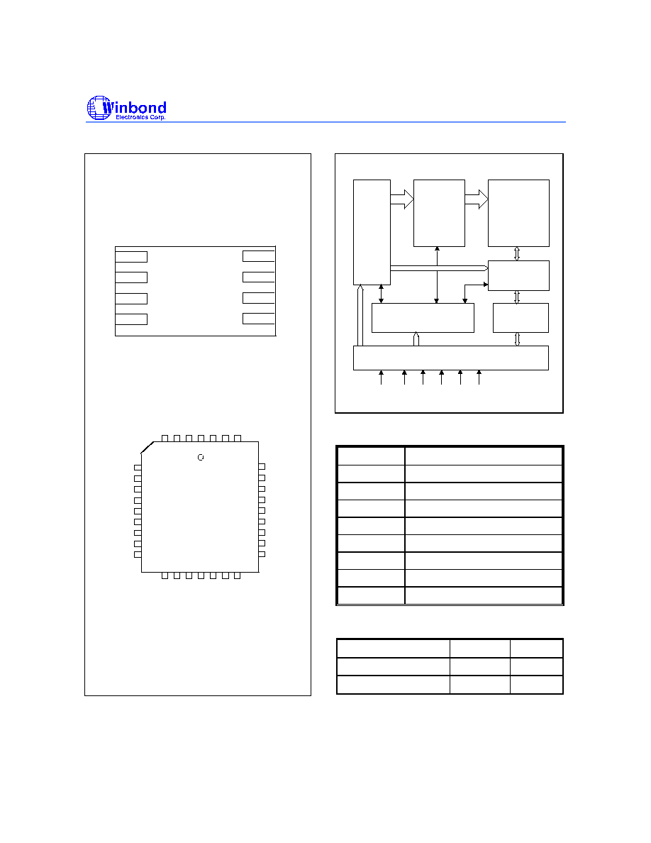
PIN CONFIGURATIONS
1
2
3
4
8
7
6
5
8L SON
Top View
VDD
#RESE
T
SCK
SI
#CE
SO
#WP
Vss
5
6
7
9
10
11
12
13
29
28
27
26
25
24
23
22
21
30
31
32
1
2
3
4
8
20
19
18
17
16
15
14
S
O
V
D
D
32L
PLCC
S
C
K
N
C
NC
NC
#WP
N
C
N
C
NC
NC
NC
NC
NC
NC
NC
#CE
N
C
V
S
S
N
C
N
C
N
C
N
C
NC
NC
NC
NC
NC
NC
#
R
E
S
E
T
SI
N
C
BLOCK DIAGRAM
SuperFlash
Cell Array
X-Decoder
Address
Buffers
and
Latches
Y-Decoder
Control Logic
I/O Buffers
and Data
Latches
Serial Interface
#CE SCK SI SO #WP #RESET
PIN DESCRIPTION
SYMBOL
PIN NAME
#CE
Chip Enable
SI
Serial Data Input
SO
Serial Data Output
SCK
Serial Clock
#WP
Write Protect
#RESET Reset
V
DD
Power Supply
V
SS
Ground
PRODUCT IDENTIFICATION
BYTE
DATA
Manufacturer's ID
0000
h
DA
h
Device ID: W45B512
0001
h
98
h

Preliminary W45B512
Publication Release Date: February 21, 2002
- 3 - Revision A1
FUNCTIONAL DESCRIPTION
Device Operation
The W45B512 uses bus cycles of 8 bits each for commands, data, and addresses to execute
operations. The operation instructions are listed in the table below. All instructions are synchronized off
a high to low transition of #CE. The first low to high transition on SCK will initiate the instruction
sequence. Inputs will be accepted on the rising edge of SCK starting with the most significant bit. Any
low to high transition on #CE before the input instruction completes will terminate any instruction in
progress and return the device to the standby mode.
Read
The Read operation outputs the data in order from the initial accessed address. While SCK is input,
the address will be incremented automatically until end (top) of the address space, then the internal
address pointer automatically increments to beginning (bottom) of the address space (00000h), and
data out stream will continue. The read data stream is continuous through all addresses until
terminated by a low to high transition on #CE.
Sector/Chip-erase Operation
The Sector-Erase operation clears all bits in the selected sector to "FF". The Chip -Erase instruction
clears all bits in the device to "FF".
Byte-program Operation
The Byte-Program operation programs the bits in the selected byte to the desired data. The selected
byte must be in the erased state ("FF") when initiating a Program operation. The data is input from bit 7
to bit 0 in order.
Software Status Operation
The Status operation determines if an Erase or Program operation is in progress. If bit 0 is at a "0" an
Erase or Program operation is in progress, the device is busy. If bit 0 is at a "1" the device is ready for
any valid operation. The status read is continuous with ongoing clock cycles until terminated by a low
to high transition on #CE.
Reset
Reset will terminate any operation, e.g., Read, Erase and Program, in progress. It is activated by a
high to low transition on the #RESET pin. The device will remain in reset condition as long as #RESET
is low. Minimum reset time is 10
µ
S. See Figure 14 for reset timing diagram. #RESET is internally
pulled-up and could remain unconnected during normal operation. After reset, the device is in standby
mode, a high to low transition on #CE is required to start the next operation. An internal power-on reset
circuit protects against accidental data writes. Applying a logic level low to #RESET during the power-
on process then changing to a logic level high when V
DD
has reached the correct voltage level will
provide additional protection against accidental writes during power on.
Read WINBOND ID/Read Device ID
The Read Manufacturer ID and Read Device ID operations read the JEDEC assigned manufacturer
identification and the manufacturer assigned device identification codes. These codes may be used to
determine the actual device resident in the system.
Preliminary W45B512
- 4 -
Write Protect
The #WP pin provides inadvertent write protection. The #WP pin must be held high for any Erase or
Program operation. The #WP pin is "don't care" for all other operations. In typical use, the #WP pin is
connected to V
SS
with a standard pull-down resistor. #WP is then driven high whenever an Erase or
Program operation is required. If the #WP pin is tied to V
DD
with a pull-up resistor, then all operations
may occur and the write protection feature is disabled. The #WP pin has an internal pull-up and could
remain unconnected when not used.
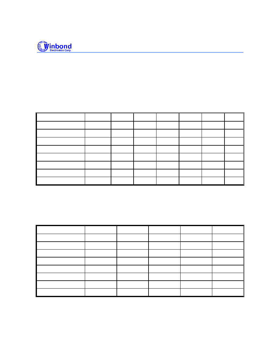
DEVICE OPERATION INSTRUCTION
BUS CYCLE
1
2
3
4
5
6
7
Operation/Type
Command Address
1
Address Address
Data
Dummy
Data
Read
FFh
A
23
-
A
16
A
15
-
A
8
A
7
-
A
0
X
X
Dout
Sector-erase
2
20h
A
23
-
A
16
A
15
-
A
8
X
Dout
X
Chip-erase
60h
X
X
X
Dout
X
Byte-program
10h
A
23
-
A
16
A
15
-
A
8
A
7
-
A
0
Din
X
Software-status
9Fh
Dout
Read Manufacture
ID
90h
X
X
A
0
=
0
DAh
Read Device ID
3
90h
X
X
A
0
=
1
98h
Notes:
1. A23
-
A16 are "Don't Care" for device.
2. A15
-
A12 are used to determine sector address, A11
-
A8 are don't care.
3. With A15
-
A1 = 0, W45B512 Device ID = 98h, is read with A0 = 1.
DEVICE OPERATION TABLE
OPERATION
SI
SO
#CE
1
#WP
#RESET
Read
X
Dout
Low
X
High
Sector-erase
X
X
Low
High
High
Chip-erase
X
X
Low
High
High
Byte-program
Din
X
Low
High
High
Software-status
X
Dout
Low
X
High
Reset2
X
X
X
X
Low
Read Manufacture ID
X
Dout
Low
X
High
Read Device ID
X
Dout
Low
X
High
Notes:
1. A high to low transition on #CE will be required to start any device operation except for Reset.
2. The #RESET low will return the device to standby and terminate any Erase or Program operation in progress.
Preliminary W45B512
Publication Release Date: February 21, 2002
- 5 - Revision A1
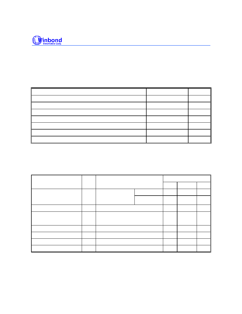
DC CHARACTERISTICS
Absolute Maximum Stress Ratings
(Applied conditions greater than those listed under "Absolute maximum Stress Ratings" may cause
permanent damage to the device. This is a stress rating only and functional operation of the device at
these conditions or conditions greater than those defined in the operational sections of this data sheet
is not implied. Exposure to absolute maximum stress rating conditions may affect device reliability.)
PARAMETER
RATING
UNIT
Temperature Under Bias
-55 to +125
∞C
Storage Temperature
-65 to +150
∞
C
D. C. Voltage on Any Pin to Ground Potential
-0.5 to V
DD
+0.5
V
Transient Voltage (<20 nS) on Any Pin to Ground Potential
-1.0 to V
DD
+1.0
V
Package Power Dissipation Capability (T
A
= 25∞ C)
1.0
W
Surface Mount Lead Soldering Temperature (3 Seconds)
240
∞C
Output Short Circuit Current
1
50
mA
Note: Exposure to conditions beyond those listed under Absolute Maximum Ratings may adversely affect the life and reliability
of the device.
DC Operating Characteristics
(V
DD
=2.7V
-
3.6V, V
SS
= 0V, T
A
= 0 to 70
∞
C)
LIMITS
PARAMETER
SYM.
TEST CONDITION
MIN.
MAX. UNITS
Program/Erase
-
30
mA
Power Supply Current
I
DD
f = 20 MHz
#CE = V
IL,
V
DD
= V
DD
Max.
Read
-
20
mA
Standby Current
I
SB
#CE = V
IHC
, V
DD
= V
DD
Max.
-
15
µ
A
Input Leakage
Output Leakage
I
LI
I
LO
V
IN
= GND to V
DD
, V
DD
= V
DD
Max.
V
OUT
= GND to V
DD
, V
DD
= V
DD
Max.
-
2
2
µ
A
µ
A
Input Low Voltage
V
IL
-0.2
0.6
V
Input High Voltage
V
IH
2.0 V
DD
+0.3
V
Output Low Voltage
V
OL
I
OL
= 1.6 mA
-
0.4
V
Output High Voltage
V
OH
I
OH
= -0.4 mA
2.4
-
V
Note: Outputs shorted for no more than one second. No more than one output shorted at a time.