
W49F002U
256K
◊
8 CMOS FLASH MEMORY
Publication Release Date: April 2000
- 1 - Revision A2
GENERAL DESCRIPTION
The W49F002U is a 2-megabit, 5-volt only CMOS flash memory organized as 256K
◊
8 bits. The
device can be programmed and erased in-system with a standard 5V power supply. A 12-volt V
PP
is
not required. The unique cell architecture of the W49F002U results in fast program/erase operations
with extremely low current consumption (compared to other comparable 5-volt flash memory
products). The device can also be programmed and erased using standard EPROM programmers.
FEATURES
∑
Single 5-volt operations:
-
5-volt Read
-
5-volt Erase
-
5-volt Program
∑
Fast Program operation:
-
Byte-by-Byte programming: 35
µ
S (typ.)
∑
Fast Erase operation: 100 mS (typ.)
∑
Fast Read access time: 70/90/120 nS
∑
Endurance: 10K cycles (typ.)
∑
Ten-year data retention
∑
Hardware data protection
∑
One 16K byte Boot Block with Lockout
protection
∑
Two 8K byte Parameter Blocks
∑
Two Main Memory Blocks (96K, 128K) Bytes
∑
Low power consumption
-
Active current: 25 mA (typ.)
-
Standby current: 20
µ
A (typ.)
∑
Automatic program and erase timing with
internal V
PP
generation
∑
End of program or erase detection
-
Toggle bit
-
Data polling
∑
Latched address and data
∑
TTL compatible I/O
∑
JEDEC standard byte-wide pinouts
∑
Available packages: 32-pin DIP and 32-pin
TSOP and 32-pin-PLCC
W49F002U
- 2 -
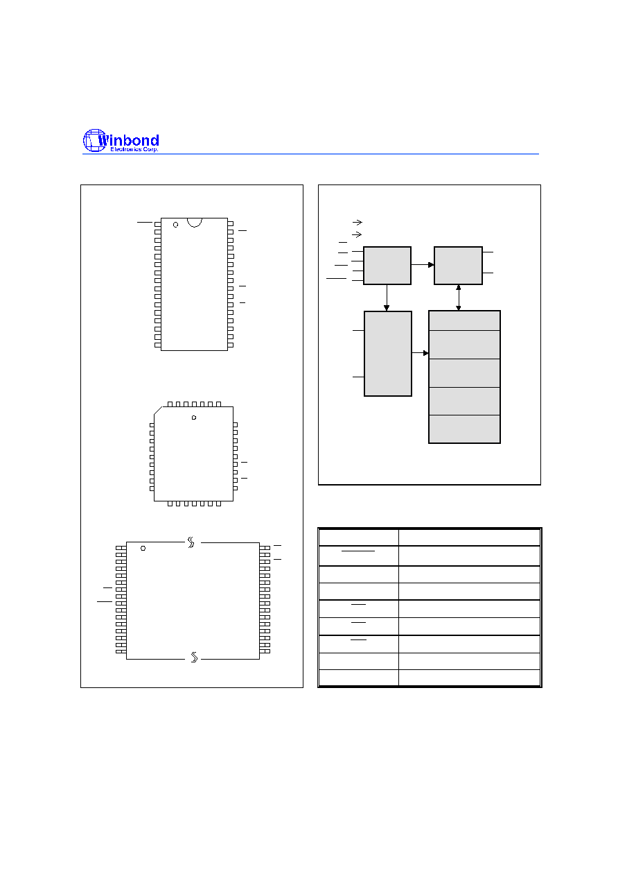
PIN CONFIGURATIONS
1
2
3
4
5
6
7
8
9
10
11
12
13
14
15
16
32
31
30
29
28
27
26
25
24
23
22
21
20
19
18
17
DQ0
DQ1
DQ2
GND
A7
A6
A5
A4
A3
A2
A1
A0
A16
A15
A12
V
WE
A14
A13
A8
A9
A11
OE
A10
CE
DQ7
DQ6
DQ5
DQ4
DQ3
DD
A17
32-pin
DIP
RESET
5
6
7
9
10
11
12
13
A7
A6
A5
A4
A3
A2
A1
A0
DQ0
29
28
27
26
25
24
23
22
21
30
31
32
1
2
3
4
8
20
19
18
17
16
15
14
D
Q
1
D
Q
2
G
N
D
D
Q
3
D
Q
4
D
Q
5
D
Q
6
A14
A13
A8
A9
A11
OE
A10
CE
DQ7
A
1
2
A
1
6
V
D
D
/
W
E
A
1
5
32-pin
PLCC
A
1
7
/
R
E
S
E
T
32-pin
TSOP
1
2
3
4
5
6
7
8
9
10
11
12
13
14
15
16
A15
A12
A7
A6
A5
A4
V
WE
A14
A13
A8
DD
A11
A9
A16
A17
RESET
A3
A2
A1
A0
DQ0
DQ1
DQ2
GND
OE
A10
CE
DQ7
DQ6
DQ5
DQ4
DQ3
32
31
30
29
28
27
26
25
24
23
22
21
20
19
18
17
BLOCK DIAGRAM
CONTROL
OUTPUT
BUFFER
DECODER
CE
OE
WE
A0
.
.
A17
.
.
DQ0
V
DD
V
SS
DQ7
3FFFF
20000
1FFFF
38000
37FFF
3A000
39FFF
00000
3C000
3BFFF
RESET
PARAMETER
BLOCK2
8K BYTES
BOOT BLOCK
16K BYTES
PARAMETER
BLOCK1
8K BYTES
MAIN MEMORY
BLOCK2
128K BYTES
MAIN MEMORY
BLOCK1
96K BYTES
PIN DESCRIPTION
SYMBOL
PIN NAME
RESET
Reset
A0
-
A17
Address Inputs
DQ0
-
DQ7
Data Inputs/Outputs
CE
Chip Enable
OE
Output Enable
WE
Write Enable
V
DD
Power Supply
GND
Ground

W49F002U
Publication Release Date: April 2000
- 3 - Revision A2
FUNCTIONAL DESCRIPTION
Read Mode
The read operation of the W49F002U is controlled by CE and OE, both of which have to be low for
the host to obtain data from the outputs. CE is used for device selection. When CE is high, the chip
is de-selected and only standby power will be consumed. OE is the output control and is used to gate
data from the output pins. The data bus is in high impedance state when either CE or OE is high.
Refer to the timing waveforms for further details.
Reset Operation
The reset input pin can be used in some application. When RESET pin is at high state, the device is
in normal operation mode. When RESET pin is at low state, it will halts the device and all outputs are
at high impedance state. As the high state re-asserted to the RESET pin, the device will return to
read or standby mode, it depends on the control signals. When the system drives the RESET pin low
for at least a period of 500 nS, the device immediately terminates any operation in progress duration
of the RESET pulse. The other function for RESET pin is temporary reset the boot block. By
applying the 12V to RESET pin, the boot block can be reprogrammed even though the boot block
lockout function is enabled.
Boot Block Operation
There is one 16K-byte boot block in this device, which can be used to store boot code. It is located in
the last 16K bytes with the address range of the boot block is 3C000(hex) to 3FFFF(hex).See
Command Code sequence for Boot Block Lockout Enable for the specific code. Once this feature is
set the data for the designated block cannot be erased or programmed (programming lockout); other
memory locations can be changed with the regular programming method. Once the boot block
programming lockout feature is activated, the chip erase function can no longer erase the boot block.
There is one condition that the lockout feature can be overridden. Just apply 12V to RESET pin, the
lockout feature will temporarily be inactivated and the block can be erased/programmed. Once the
RESET pin return to TTL level, the lockout feature will be activated again.
In order to detect whether the boot block feature is set on the 16K-bytes block, users can perform
software command code sequence: enter the product identification mode (see Command Codes for
Identification/Boot Block Lockout Detection for specific code), and then read from address "0002
(hex)". If the DQ
0
of output data is "1," the boot block programming lockout feature is activated; if the
DQ0
of output data is "0 ," the lockout feature is inactivated and the block can be
erased/programmed.
To return to normal operation, perform a three-byte command code sequence (or an alternate single-
byte command) to exit the identification mode. For the specific code, see Command Code for
Identification/Boot Block Lockout Detection.
Chip Erase Operation
The chip-erase mode can be initiated by a six-byte command code sequence. After the command
loading cycle, the device enters the internal chip erase mode, which is automatically timed and will be
completed as fast as 100 mS (typical). The host system is not required to provide any control or
timing during this operation. The entire memory array will be erased to FF hex. by the chip erase

W49F002U
- 4 -
operation if the boot block programming lockout feature is not activated. Once the boot block lockout
feature is activated, the whole chip erase function will erase the two main memory blocks and the two
parameter blocks but not the boot block. The device will automatically return to normal read mode
after the erase operation. Data polling and/or Toggle Bits can be used to detect end of erase cycle.
Sector Erase Operation
There are four sectors: two main memory blocks and two parameters blocks which can be erased
individually by initiating a six-byte command code sequence. Sector address is latched on the falling
edge of WE signal in the sixth cycle while the data input "30(hex)" is latched at the rising edge of WE
in this cycle. After the command loading cycle, the device enters the internal sector erase mode,
which is automatically timed and will be completed as fast as 100 mS (typical). The host system does
not require to provide any control or timing during this operation. The device will automatically return
to normal read mode after the erase operation. Data polling and/or Toggle Bits can be used to detect
the end of erase cycle.
When different sector address is loaded in the sixth cycle for sector erase command, the
correspondent sectors will be erased automatically; that these sections will be erased independedntly.
For detail sector to be erased information, please refer to the Table of Command Definition.
Program Operation
The W49F002U is programmed on a byte-by-byte basis. Program operation can only change logical
data "1" to logical data "0". The erase operation (changed entire data in two main memory blocks and
two parameter blocks and/or boot block from "0" to "1") is needed before programming.
The program operation is initiated by a 4-byte command code sequence (see Command Codes for
Byte Programming). The device will internally enter the program operation immediately after the byte-
program command is entered. The internal program timer will automatically time-out (50
µ
S max. -
T
BP
). Once completed, the device returns to normal read mode. Data polling and/or Toggle Bits can
be used to detect end of program cycle.
Hardware Data Protection
The integrity of the data stored in the W49F002U is also hardware protected in the following ways:
(1) Noise/Glitch Protection: A WE pulse of less than 15 nS in duration will not initiate a write cycle.
(2) V
DD
Power Up/Down Detection: The programming operation is inhibited when V
DD
is less than
2.5V typical.
(3) Write Inhibit Mode: Forcing OE low, CE high, or WE high will inhibit the write operation. This
prevents inadvertent writes during power-up or power-down periods.
(4) V
DD
power-on delay: When V
DD
has reached its sense level, the device will automatically time-out
5 mS before any write (erase/program) operation.
Data Polling (DQ
7
)- Write Status Detection
The W49F002U includes a data polling feature to indicate the end of a program or erase cycle.
When the W49F002U is in the internal program or erase cycle, any attempt to read DQ
7
of the last
byte loaded will receive the complement of the true data. Once the program or erase cycle is
completed, DQ
7
will show the true data. Note that DQ
7
will show logical "0" during the erase cycle,
and become logical "1" or true data when the erase cycle has been completed.
W49F002U
Publication Release Date: April 2000
- 5 - Revision A2
Toggle Bit (DQ
6
)- Write Status Detection
In addition to data polling, the W49F002U provides another method for determining the end of a
program cycle. During the internal program or erase cycle, any consecutive attempts to read DQ
6
will
produce alternating 0's and 1's. When the program or erase cycle is completed, this toggling between
0's and 1's will stop. The device is then ready for the next operation.
Product Identification
The product ID operation outputs the manufacturer code and device code. Programming equipment
automatically matches the device with its proper erase and programming algorithms.
The manufacturer and device codes can be accessed by software or hardware operation. In the
software access mode, a three-byte (or JEDEC 3-byte) command sequence can be used to access
the product ID. A read from address 0000H outputs the manufacturer code DA(hex). A read from
address 0001H outputs the device code 0B(hex). The product ID operation can be terminated by a
three-byte command code sequence or an alternate one-byte command code sequence (see
Command Definition table).
In the hardware access mode, access to the product ID is activated by forcing CE and OE low, WE
high, and raising A9 to 12 volts.
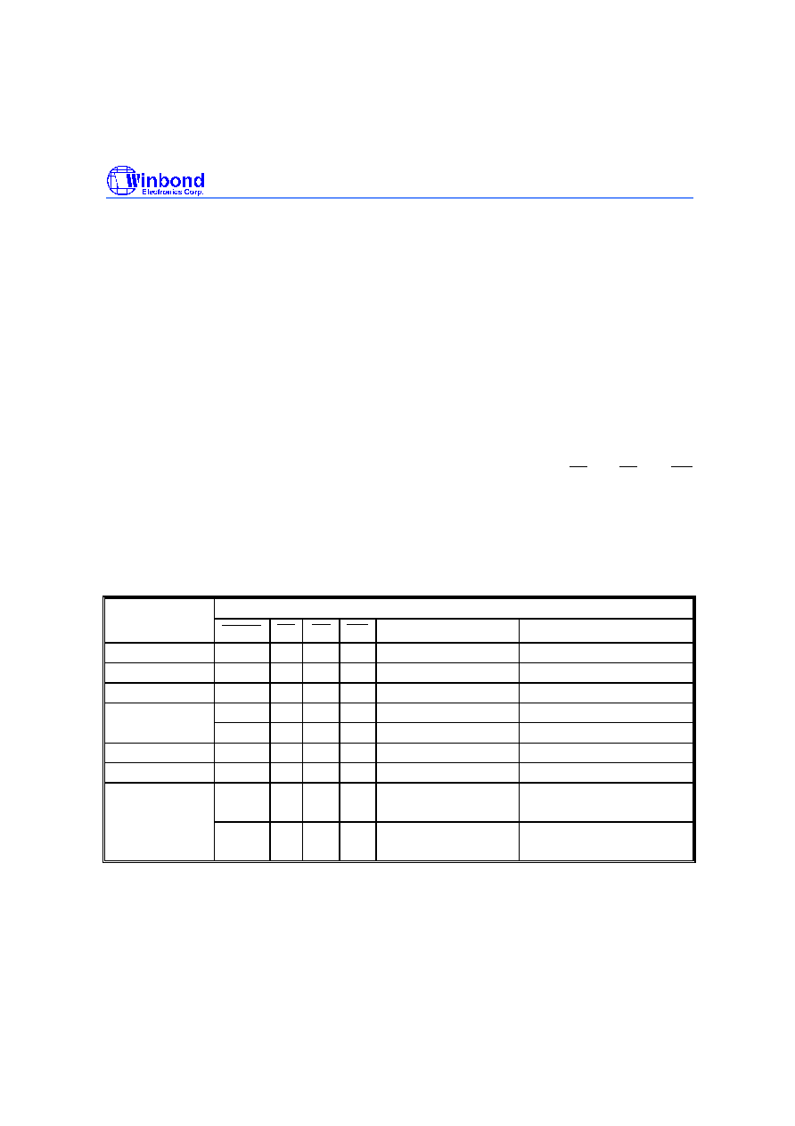
TABLE OF OPERATING MODES
Operating Mode Selection
(V
HH
= 12V
±
5
%
)
MODE
PINS
RESET
CE
OE
WE
ADDRESS
DQ.
Read
V
IH
V
IL
V
IL
V
IH
A
IN
Dout
Write
V
IH
V
IL
V
IH
V
IL
A
IN
Din
Standby
V
IH
V
IH
X
X
X
High Z
Write Inhibit
V
IH
X
V
IL
X
X
High Z/DOUT
V
IH
X
X
V
IH
X
High Z/DOUT
Output Disable
V
IH
X
V
IH
X
X
High Z
Reset Mode
V
IL
X
X
X
X
High Z
Product ID
V
IH
V
IL
V
IL
V
IH
A0 = V
IL
; A1
-
A17 = V
IL
;
A9 = V
HH
Manufacturer Code DA (Hex)
V
IH
V
IL
V
IL
V
IH
A0 = V
IH
; A1
-
A17 = V
IL
;
A9 = V
HH
Device Code 0B (Hex)