 | –≠–ª–µ–∫—Ç—Ä–æ–Ω–Ω—ã–π –∫–æ–º–ø–æ–Ω–µ–Ω—Ç: W49L401 | –°–∫–∞—á–∞—Ç—å:  PDF PDF  ZIP ZIP |

W49L401(T)
256K
◊
16 CMOS FLASH MEMORY
Publication Release Date: August 16, 2002
- 1 - Revision A4
1. GENERAL DESCRIPTION
The W49L401(T) is a 4-megabit, 3.3-volt only CMOS flash memory organized as 256K
◊
16 bits. The
device can be programmed and erased in-system with a standard 3.3-volt power supply. A 12-volt V
PP
is not required. The unique cell architecture of the W49L401(T) results in fast program/erase
operations with extremely low current consumption (compared to other comparable 3.3-volt flash
memory products). The device can also be programmed and erased using standard EPROM
programmers.
2. FEATURES
∑
Single Voltage operations:
-
3.0
-
3.6V Read/Erase/Program
∑
Fast Program operation:
-
Word-by-Word programming: 30
µ
S (typ.)
∑
Fast Erase operation:
-
Page/Block Erase time: 50 mS (typ.)
-
Chip Erase time: 200 mS (typ.)
∑
Fast Read access time: 70 nS
∑
Endurance: 10K cycles (typ.)
∑
Twenty-year data retention
∑
Hardware data protection
∑
Block configuration
-
One 8K-word boot block with lockout
protection
-
Two 4K-word parameter blocks
-
One 16K-word main memory array block
-
Seven 32K-word main memory array blocks
-
128 uniform 2K-word pages
∑
Optional Uniform Page configuration
∑
Low power consumption
-
Active current: 10 mA (typ.)
-
Standby current: 5
µ
A (typ.)
∑
Automatic program and erase timing with
internal V
PP
generation
∑
End of program or erase detection
-
Toggle bit
-
Data polling
∑
RY/#BY open-drain output provides hardware
end-of-write detection
∑
Hardware #RESET pin
∑
Latched address and data
∑
TTL compatible I/O
∑
JEDEC standard word-wide pinouts
∑
Available packages: 44-pin SOP, 48-pin TSOP
W49L401(T)
- 2 -
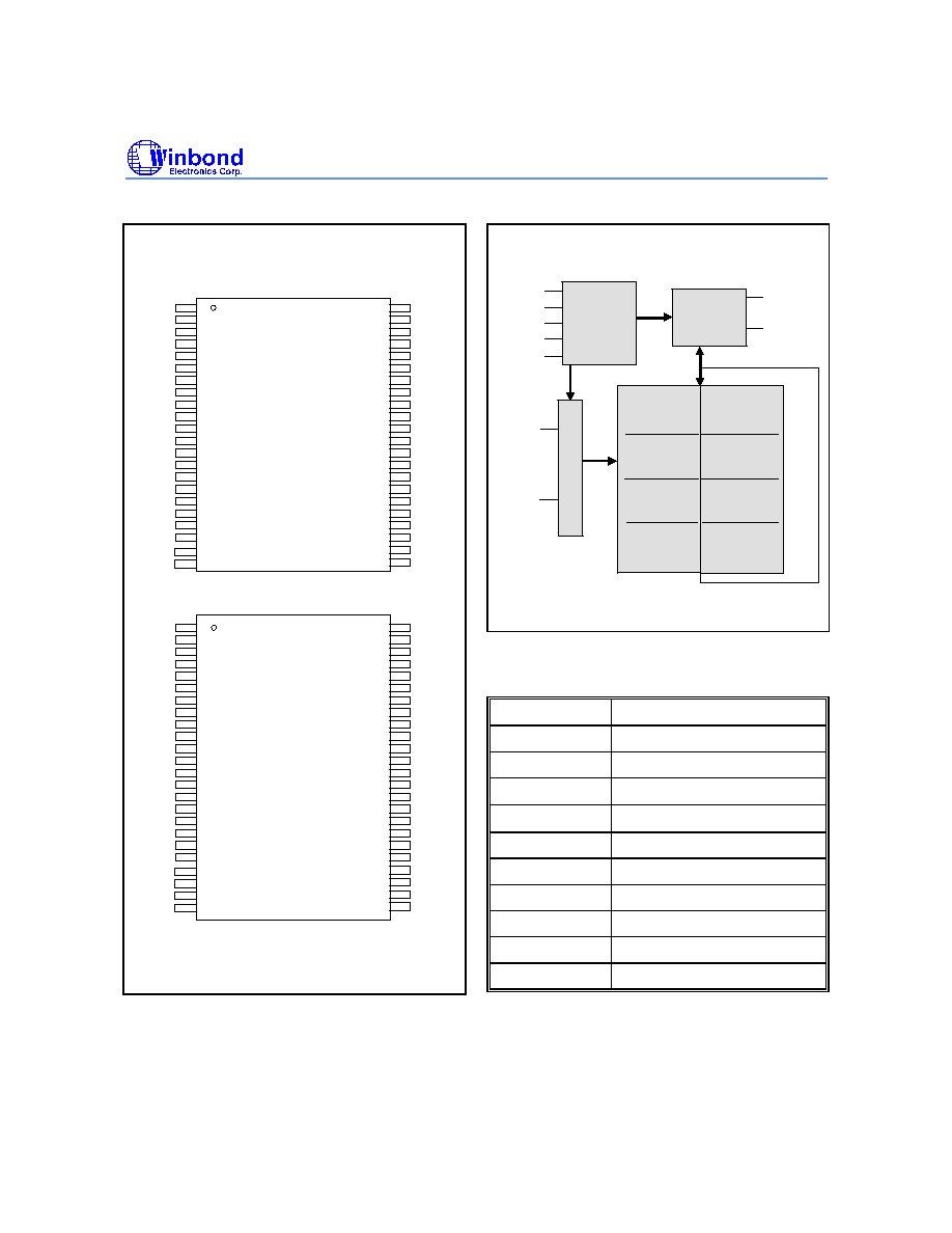
3. PIN CONFIGURATIONS
1
2
3
4
5
6
7
8
9
10
11
12
13
14
15
16
17
18
19
20
40
39
38
37
36
35
34
33
32
31
30
29
28
27
26
25
DQ15
A9
A10
A11
A12
A13
A14
A15
#OE
48-pin
TSOP
24
23
A16
#WE
#CE
A7
A6
A5
A4
A3
A2
A1
A0
21
22
48
47
46
45
44
43
42
41
NC
#RESET
NC
NC
A8
DQ11
DQ3
DQ10
DQ2
DQ9
DQ1
DQ8
DQ0
V
DD
DQ7
DQ14
DQ6
DQ13
DQ5
DQ12
DQ4
NC
1
2
3
4
5
6
7
8
9
10
11
12
13
14
15
16
17
18
19
20
DQ15
#OE
44-pin
SOP
24
23
A16
#CE
A0
21
22
40
39
38
37
36
35
34
33
32
31
30
29
28
27
44
43
42
41
A7
A6
A5
A4
A3
A2
A1
A9
A10
A11
A12
A13
A14
A15
#WE
#RESET
A8
DQ11
DQ3
DQ10
DQ2
DQ9
DQ1
DQ8
DQ0
V
DD
DQ7
DQ14
DQ6
DQ13
DQ5
DQ12
DQ4
NC
26
25
V
SS
V
SS
V
SS
V
SS
A17
A17
NC
RY/#BY
RY/#BY
NC
NC
4. BLOCK DIAGRAM
CONTROL
OUTPUT
BUFFER
D
E
C
O
D
E
R
#CE
#OE
#WE
A0
.
.
A17
.
.
DQ0
DQ15
#RESET
BOOT BLOCK
8K WORDS
PARAMETER
BLOCK2
4K WORDS
PARAMETER
BLOCK1
4K WORDS
3FFFF
04000
03FFF
03000
02FFF
02000
01FFF
00000
W49L401
MAIN MEMORY
240K WORDS
BOOT BLOCK
8K WORDS
PARAMETER
BLOCK2
4K WORDS
PARAMETER
BLOCK1
4K WORDS
3FFFF
3E000
3DFFF
3D000
3CFFF
3C000
3BFFF
00000
W49L401T
RY/#BY
(1x16K WORDS
7x32K WORDS)
MAIN MEMORY
240K WORDS
(1x16K WORDS
7x32K WORDS)
5. PIN DESCRIPTION
SYMBOL
PIN NAME
#RESET
Reset
RY/#BY
Ready/#Busy Output
A0
-
A17
Address Inputs
DQ0
-
DQ15 Data Inputs/Outputs
#CE
Chip Enable
#OE
Output Enable
#WE
Write Enable
V
DD
Power Supply
V
SS
Ground
NC
No Connection

W49L401(T)
Publication Release Date: August 16, 2002
- 3 - Revision A4
6. FUNCTIONAL DESCRIPTION
Read Mode
The read operation of the W49L401(T) is controlled by #CE and #OE, both of which have to be low for
the host to obtain data from the outputs. #CE is used for device selection. When #CE is high, the chip
is de-selected and only standby power will be consumed. #OE is the output control and is used to gate
data to the output pins. The data bus is in high impedance state when either #CE or #OE is high. Refer
to the timing waveforms for further details.
Reset Operation
The #RESET
input pin can be used in some application. When #RESET pin is at high state, the device
is in normal operation mode. When #RESET pin is driven low for at least a period of T
RP
, it will halt the
device and all outputs are at high impedance state. The device also resets the internal state machine
to read array data. The operation that was interrupted should be reinitiated once the device is ready to
accept another command sequence to assure data integrity. As the high state re-asserted to the
#RESET pin, the device will return to read or standby mode, it depends on the control signals. The
system can read data T
RH
after the #RESET
pin returns to V
IH
. The other function for #RESET pin is
temporary reset the boot block. By applying the 12V to #RESET
pin, the boot block can be
reprogrammed even though the boot block lockout function is enabled.
Boot Block Operation
There is one 8K-word boot block in this device, which can be used to store boot code. It is located in
the first 8K words (for W49L401T, located in the last 8K words) of the memory with the address range
from 0000(hex) to 1FFF(hex). (for W49L401T, address range from 3E000h to 3FFFFh)
See Command Codes for Boot Block Lockout Enable for the specific code. Once this feature is set, the
data for the designated block cannot be erased or programmed (programming lockout); the regular
programming method can change the data in other memory locations.
There is one condition that the lockout feature can be over-ridden. Just apply 12V to #RESET
pin, the
lockout feature will temporarily be inactivated and the boot block can be erased/programmed. Once the
#RESET
pin returns to CMOS/TTL level, the lockout feature will be activated again.
In order to detect whether the boot block feature is set on the 8K-words block, users can perform
software command sequence: enter the product identification mode (see Command Codes for
Identification/Boot Block Lockout Detection for specific code), and then read from address "0002 hex".
If the output data in DQ0 is "1", the boot block programming lockout feature is activated; if the output
data in DQ0 is "0", the lockout feature is inactivated and the block can be erased/programmed.
To return to normal operation, perform a three-byte command sequence (or an alternate single-word
command) to exit the identification mode. For the specific code, see Command Codes for
Identification/Boot Block Lockout Detection.
Chip Erase Operation
The chip-erase mode can be initiated by a six-word command sequence. After the command loading
cycle, the device enters the internal chip erase mode, which is automatically timed and will be
completed in a fast 200 mS (typical). The host system is not required to provide any control or timing
during this operation. The entire memory array will be erased to FFFF(hex) by the chip erase operation
if the boot block programming lockout feature is not activated. Once the boot block lockout feature is
activated, the chip erase function will erase all the blocks/pages except the boot block.

W49L401(T)
- 4 -
Block/Page Erase Operation
The W49L401(T) provides both uniform small page (2K-word) and non-symmetrical block
(4K/8K/16K/32K-word) erase capabilities for versatile Flash applications.
Each block or page can be erased individually by initiating a six-word command sequence. The block
address (BA) or page address (PA) is latched on the falling #WE edge of the sixth cycle while the
XX30/XX50(hex) data input command is latched at the rising edge of #WE. After the command loading
cycle, the device enters the internal block/page erase mode, which is automatically timed and will be
completed in a fast 50 mS (typical). The host system is not required to provide any control or timing
during this operation. The device will automatically return to normal read mode after the erase
operation completed. Data-polling, Toggle-Bit and/or RY/#BY pin can be used to detect end of erase
cycle.
The bootblock (8K-words) consists of 4 corresponding uniform pages of 2K-words each. When the
boot block lockout feature is activated, any page/block erase command with the associated PA/BA
within the bootblock address range (0000-01FFF for W49L401, and 3E000-3FFFF for W49L401T) will
be ignored and the device will return to read mode without any data changes.
Program Operation
The W49L401(T) is programmed on a word-by-word basis. Program operation can only change logical
data "1" to logical data "0" The erase operation (changed entire data in individual page/block or whole
chip from "0" to "1") is needed before programming.
The program operation is initiated by a 4-word command cycle (see Command Codes for Word
Programming). The device will internally enter the program operation immediately after the word-
program command is entered. The internal program timer will automatically time-out (50
µ
S max. -
T
BP
) once completed and return to normal read mode. Data_polling, Toggle_Bit and/or RY/#BY pin
can be used to detect end of program cycle.
Hardware Data Protection
The integrity of the data stored in the W49L401(T) is also hardware protected in the following ways:
(1) Noise/Glitch Protection: A #WE pulse of less than 10 nS in duration will not initiate a write cycle.
(2) V
DD
Power Up/Down Detection: The programming operation and read are inhibited when V
DD
is
less than 1.8V typical.
(3) Write Inhibit Mode: Forcing #OE low, #CE high, or #WE high will inhibit the write operation. This
prevents inadvertent writes during power-up or power-down periods.
(4) V
DD
power-on delay: When V
DD
has reached its sense level, the device will automatically time-out
10 mS before any write (erase/program) operation.
Data Polling (DQ
7
)- Write Status Detection
The W49L401(T) includes a data polling feature to indicate the end of a program or erase cycle.
When the W49L401(T) is in the internal program or erase cycle, any attempt to read DQ
7
of the last
word loaded will receive the complement of the true data. Once the program or erase cycle is
completed, DQ
7
will show the true data. Note that, DQ
7
will show logical "0" during the erase cycle.
And it will become logical "1" or true data when the erase cycle is completed.
Toggle Bit (DQ
6
)- Write Status Detection
In addition to data polling, the W49L401(T) provides another method for determining the end of a
program cycle. During the internal program or erase cycle, any consecutive attempts to read DQ
6
will
W49L401(T)
Publication Release Date: August 16, 2002
- 5 - Revision A4
produce alternating 0's and 1's. When the program or erase cycle is completed, this toggling between
0's and 1's will stop. The device is then ready for the next operation.
Ready/#Busy
The W49L401(T) also provides the hardware method to detect the completion of program/erase cycle .
The RY/#BY
output pin will be asserted low (busy) during programming/erasing operations, and will be
released to high state by an external pull-up (ready) when internal program/erase cycle is completed.
This is an open-drain output pin for easy external connection.
Product Identification
The product ID operation outputs the manufacturer code and device code. Programming equipment
automatically matches the device with its proper erase and programming algorithms.
The manufacturer and device codes can be accessed by software or hardware operation. In the
software access mode, a six-word (or JEDEC 3-word) command sequence can be used to access the
product ID. A read from address 0000H outputs the manufacturer code, 00DA(hex). A read from
address 0001(hex) outputs the device code, 003D(hex) for bottom boot (and TBD for top boot). The
product ID operation can be terminated by a three-word command sequence or an alternative one-
word command sequence (see Command Definition table).
In the hardware access mode, access to the product ID is activated by forcing #CE and #OE low, #WE
high, and raising A9 to V
HH
(12V
+
/
-
0.5V).
Table of Operating Modes
Operating Mode Selection
(V
HH
= 12V
±
0.5V)
PINS
MODE
#CE #OE #WE #RESET
ADDRESS
DQ.
Read
V
IL
V
IL
V
IH
V
IH
A
IN
Dout
Erase/Program
V
IL
V
IH
V
IL
V
IH
A
IN
Din
Standby
V
IH
X
X
V
IH
X
High Z
V
IH
X
X
V
IH
X
High Z
X
V
IL
X
V
IH
X
High Z/D
OUT
Erase/Program
Inhibit
X
X
V
IH
V
IH
X
High Z/D
OUT
Output Disable
X
V
IH
X
V
IH
X
High Z
A0 = V
IL
;
A1
-
A15 = V
IL
;
A9 = V
HH
Manufacturer Code
00DA (Hex)
Product ID
V
IL
V
IL
V
IH
V
IH
A0 = V
IH
;
A1
-
A15 = V
IL
;
A9 = V
HH
Device Code
003D (Hex) for bottom
TBD for Top
Reset
X
X
X
V
IL
X
High Z
W49L401(T)
- 6 -
Table of Software Command Definition
1ST CYCLE 2ND CYCLE 3RD CYCLE 4TH CYCLE 5TH CYCLE 6TH CYCLE
COMMAND
DESCRIPTION
NO. OF
Cycles
Addr. Data
Addr. Data
Addr. Data
Addr. Data
Addr. Data
Addr. Data
Chip Erase
6
5555 AA 2AAA 55 5555 80 5555 AA 2AAA 55 5555 10
Block Erase
6
5555 AA 2AAA 55 5555 80 5555 AA 2AAA 55 BA
(5)
30
Page Erase
6
5555 AA 2AAA 55 5555 80 5555 AA 2AAA 55 PA
(4)
50
Word Program
4
5555 AA 2AAA 55 5555 A0 A
IN
D
IN
Boot Block Lockout
6
5555 AA 2AAA 55 5555 80 5555 AA 2AAA 55 5555 40
Product ID Entry
3
5555 AA 2AAA 55 5555 90
Product ID Exit
(1)
3
5555 AA 2AAA 55 5555 F0
Product ID Exit
(1)
1
XXXX F0
Notes:
1. Address Format: A14
-
A0 (Hex); Data Format: DQ15
-
DQ8 (Don't Care); DQ7
-
DQ0 (Hex)
2. If any invalid command or read cycle (both #CE & #OE are active low) is inserted during any of the above software command
sequence, it will abort the operation and the device return to read mode.
3. Either one of the two Product ID Exit commands can be used, and Read mode is resumed after this command executed.
4. PA: Page Address
W49L401
W49L401T
PA = 00000h to 007FFh for Page0
PA = 3F800h to 3FFFFh for Page0
PA = 00800h to 00FFFh for Page1
PA = 3F000h to 3F7FFh for Page1
PA = 01000h to 017FFh for Page2
PA = 3E800h to 3EFFFh for Page2
PA = 01800h to 01FFFh for Page3
PA = 3E000h to 3E7FFh for Page3
PA = 02000h to 027FFh for Page4
PA = 3D800h to 3DFFFh for Page4
PA = 02800h to 02FFFh for Page5
PA = 3D000h to 3D7FFh for Page5
...
...
...
...
...
...
PA = 3D000h to 3D7FFh for Page122
PA = 02800h to 02FFFh for Page122
PA = 3D800h to 3DFFFh for Page123
PA = 02000h to 027FFh for Page123
PA = 3E000h to 3E7FFh for Page124
PA = 01800h to 01FFFh for Page123
PA = 3E800h to 3EFFFh for Page125
PA = 01000h to 017FFh for Page125
PA = 3F000h to 3F7FFh for Page126
PA = 00800h to 00FFFh for Page126
PA = 3F800h to 3FFFFh for Page127
PA = 00000h to 007FFh for Page127
5. BA: Block Address
W49L401
W49L401T
BA = 00000h to 01FFFh for Boot Block (8KW)
BA = 3E000h to 3FFFFh for Boot Block (8KW)
BA = 02XXXh for Parameter Block1 (4KW)
BA = 3DXXXh for Parameter Block1 (4KW)
BA = 03XXXh for Parameter Block2 (4KW)
BA = 3CXXXh for Parameter Block2 (4KW)
BA = 04000h to 07FFFh for Main Memory Block1 (16KW) BA = 38000h to 3BFFFh for Main Memory Block1 (16KW)
BA = 08000h to 0FFFFh for Main Memory Block2 (32KW) BA = 30000h to 37FFFh for Main Memory Block2 (32KW)
BA = 10000h to 17FFFh for Main Memory Block3 (32KW) BA = 28000h to 2FFFFh for Main Memory Block2 (32KW)
BA = 18000h to 1FFFFh for Main Memory Block4 (32KW) BA = 20000h to 27FFFh for Main Memory Block3 (32KW)
BA = 20000h to 27FFFh for Main Memory Block5 (32KW) BA = 18000h to 1FFFFh for Main Memory Block4 (32KW)
BA = 28000h to 2FFFFh for Main Memory Block6 (32KW) BA = 10000h to 17FFFh for Main Memory Block5 (32KW)
BA = 30000h to 37FFFh for Main Memory Block7 (32KW) BA = 08000h to 07FFFh for Main Memory Block7 (32KW)
BA = 38000h to 3FFFFh for Main Memory Block8 (32KW) BA = 00000h to 07FFFh for Main Memory Block8 (32KW)
W49L401(T)
Publication Release Date: August 16, 2002
- 7 - Revision A4
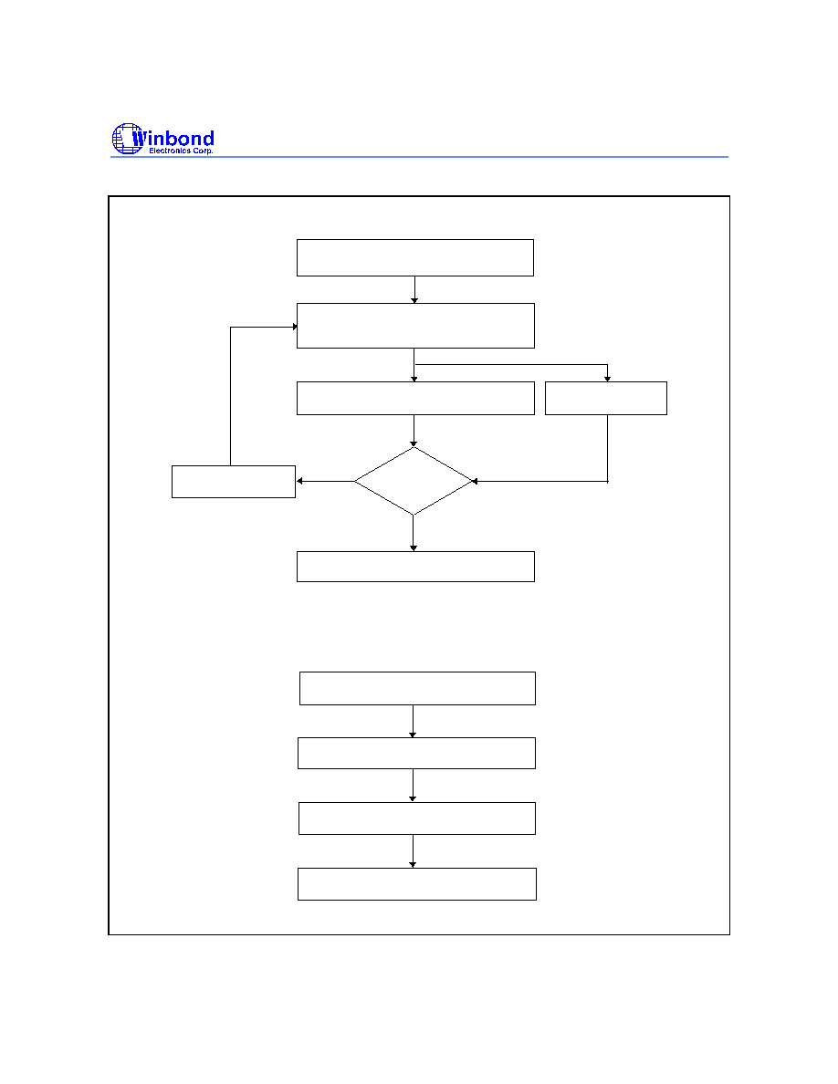
Embedded Programming Algorithm
Start
Write Program Command Sequence
(see below)
Increment Address
Programming Completed
#Data Polling/ Toggle bit
Last Address
?
No
Yes
5555H/AAH
2AAAH/55H
5555H/A0H
Program Address/Program Data
Program Command Sequence (Address/Command):
Pause T
EC
/T
SEC
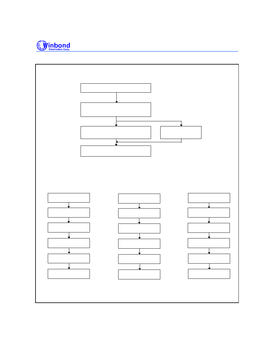
W49L401(T)
- 8 -
Embedded Erase Algorithm
Start
Write Erase Command Sequence
(see below)
Erasure Completed
#Data Polling or Toggle
Bit
Successfully Completed
5555H/AAH
5555H/AAH
2AAAH/55H
2AAAH/55H
5555H/80H
5555H/10H
Chip Erase Command Sequence
(Address/Command):
5555H/AAH
5555H/AAH
2AAAH/55H
2AAAH/55H
5555H/80H
Block Address/30H
(Address/Command):
5555H/AAH
5555H/AAH
2AAAH/55H
2AAAH/55H
5555H/80H
PageAddress/50H
Individual PageErase
(Address/Command):
Individual BlockErase
Command Sequence
Command Sequence
Pause T
EC
/T
SEC
W49L401(T)
Publication Release Date: August 16, 2002
- 9 - Revision A4
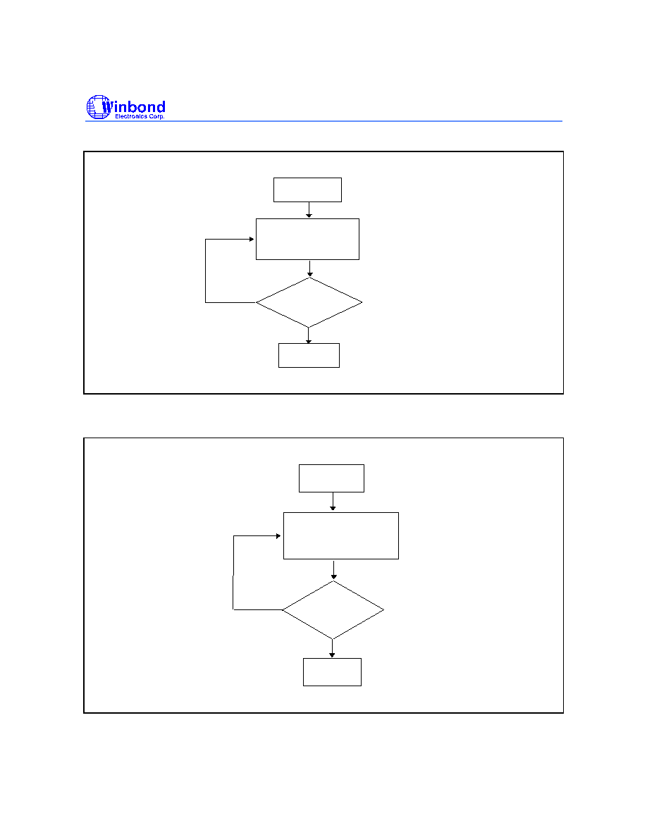
Embedded #Data Polling Algorithm
Start
Read Byte
(DQ0 - DQ7)
Address = VA
Pass
DQ7 = Data
?
Yes
No
VA = Byte address for programming
= Any of the sector addresses within
the sector being erased during sector
erase operation
= Valid address equals any sector group
address during chip erase
Embedded Toggle Bit Algorithm
Start
Read Byte
(DQ0 - DQ7)
Address = Don't Care
DQ6 = Toggle
?
Yes
No
Pass

W49L401(T)
- 10 -
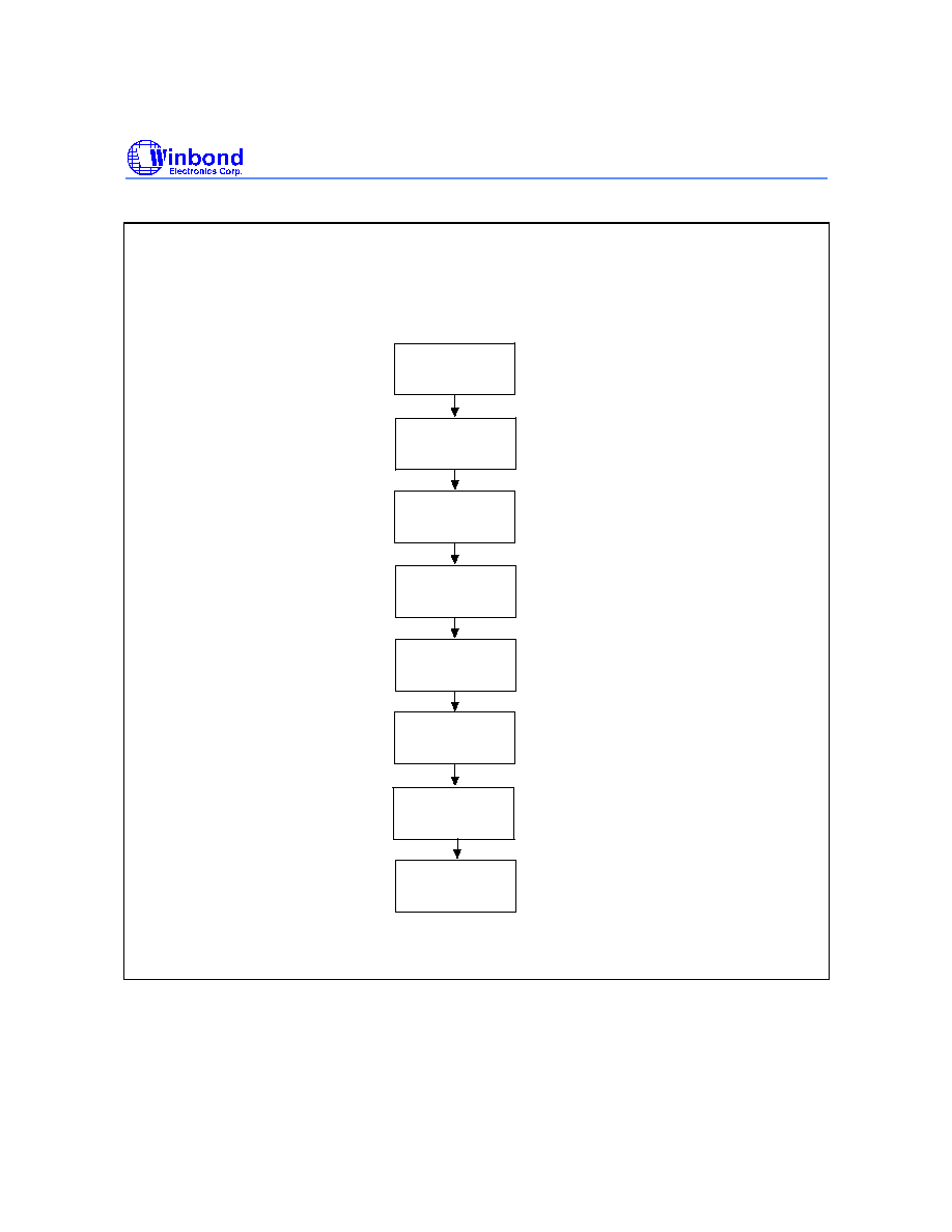
Product
Identification
Entry (1)
Load data 55
to
address 2AAA
Load data 90
to
address 5555
Pause 10 S
Product
Identification
and Boot Block
Lockout Detection
Mode (3)
Read address = 0000
data = 00DA
Read address = 0001
data = 003D for bottom
Read address = 0002
data in DQ0 =1/0
(4)
Product
Identification Exit(6)
Load data 55
to
address 2AAA
Load data F0
to
address 5555
Normal Mode
(5)
(2)
(2)
Load data AA
to
address 5555
µ
Load data AA
to
address 5555
Pause 10 S
µ
TBD for top
Software Product Identification and Boot Block Lockout Detection Acquisition
Flow
W49L401(T)
Publication Release Date: August 16, 2002
- 11 - Revision A4
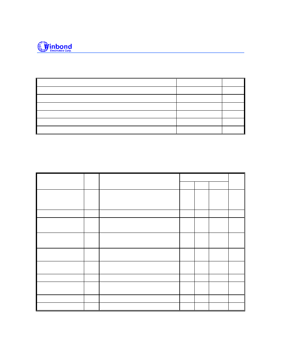
Boot Block Lockout Enable Acquisition Flow
Boot Block Lockout
Feature Set Flow
Load data AA
to
address 5555
Load data 55
to
address 2AAA
Load data 80
to
address 5555
Load data AA
to
address 5555
Load data 55
to
address 2AAA
Load data 40
to
address 5555
Pause 200 mS
Exit
W49L401(T)
- 12 -
7. DC CHARACTERISTICS
Absolute Maximum Ratings
PARAMETER
RATING
UNIT
Power Supply Voltage to V
ss
Potential
-0.5 to +4.6
V
Operating Temperature
0 to +70
∞
C
Storage Temperature
-65 to +150
∞
C
D.C. Voltage on Any Pin to Ground Potential except A9 or #RESET
-0.5 to V
DD
+1.0
V
Transient Voltage (<20 nS) on Any Pin to Ground Potential
-1.0 to V
DD
+1.0
V
Voltage on A9 or #RESET Pin to Ground Potential
-0.5 to 12.5
V
Note: Exposure to conditions beyond those listed under Absolute Maximum Ratings may adversely affect the life and reliability
of the device.
DC Operating Characteristics
(V
DD
= 3.0 ~ 3.6V, V
SS
= 0V, T
A
= 0 to 70
∞
C)
LIMITS
PARAMETER
SYM.
TEST CONDITIONS
MIN. TYP. MAX.
UNIT
V
DD
Current - Read
I
CC
#CE = #OE = V
IL
, #WE = V
IH
,
all DQs open
Address inputs = V
IL
/V
IH
, at f = 5 MHz
-
10
20
mA
V
DD
Current - Write
I
CCW
#CE = #WE = V
IL
, #OE = V
IH
-
15
25
mA
Standby V
DD
Current (TTL input)
I
SB
1
#CE = V
IH
, all DQs open
Other inputs = V
IL
/V
IH
-
-
1
mA
Standby V
DD
Current
(CMOS input)
I
SB
2
#CE = V
DD
-0.3V, all DQs open
Other inputs = V
DD
-0.3V / V
SS
-
5
50
µ
A
Input Leakage
Current
I
LI
V
IN
= V
SS
to V
DD
-
-
10
µ
A
Output Leakage
Current
I
LO
V
OUT
= V
SS
to V
DD
-
-
10
µ
A
Input Low Voltage
V
IL
-
-0.2
-
0.8
V
Input High Voltage
V
IH
-
2.0
-
V
DD
+0.3
V
Output Low Voltage
V
OL
I
OL
= 2.1 mA
-
-
0.45
V
Output High Voltage
V
OH
I
OH
= -0.4 mA
2.4
-
-
V
W49L401(T)
Publication Release Date: August 16, 2002
- 13 - Revision A4
Power-up Timing
PARAMETER
SYMBOL
TYPICAL
UNIT
Power-up to Read Operation
T
PU
. READ
200
µ
S
Power-up to Write Operation
T
PU
. WRITE
10
mS
Capacitance
(V
DD
= 3.3V, T
A
= 25
∞
C, f = 1 MHz)
PARAMETER
SYMBOL
CONDITIONS
MAX.
UNIT
I/O Pin Capacitance
C
I/O
V
I/O
= 0V
12
pf
Input Capacitance
C
IN
V
IN
= 0V
6
pf
8. AC CHARACTERISTICS
AC Test Conditions
PARAMETER
CONDITIONS
Input Pulse Levels
0V to 0.9 V
DD
Input Rise/Fall Time
< 5 nS
Input/Output Timing Level
1.5V/1.5V
Output Load
1 TTL Gate and C
L
= 30 pF
AC Test Load and Waveform
+3.3V
1.8K
1.3K
D
OUT
(Including Jig and Scope)
Input
0V
Test Point
Test Point
1.5V
1.5V
Output
30 pF
0.9V
DD

W49L401(T)
- 14 -
AC Characteristics, continued
Read Cycle Timing Parameters
(V
DD
= 3.0 ~ 3.6V, V
SS
= 0V, T
A
= 0 to 70
∞
C)
70 nS
PARAMETER
SYMBOL
MIN.
MAX.
UNIT
Read Cycle Time
T
RC
70
-
nS
Chip Enable Access Time
T
CE
-
70
nS
Address Access Time
T
AA
-
70
nS
Output Enable Access Time
T
OE
-
35
nS
#CE Low to Active Output
T
CLZ
0
-
nS
#OE Low to Active Output
T
OLZ
0
-
nS
#CE High to High-Z Output
T
CHZ
-
25
nS
#OE High to High-Z Output
T
OHZ
-
25
nS
Output Hold from Address Change
T
OH
0
-
nS
Note: The parameter of T
CLZ
, T
OLZ
, T
CHZ
, T
OHZ
are characterized only and is not 100% tested.
Write Cycle Timing Parameters
PARAMETER
SYMBOL
MIN.
TYP.
MAX.
UNIT
Address Setup Time
T
AS
10
-
-
nS
Address Hold Time
T
AH
100
-
-
nS
#WE and #CE Setup Time
T
CS
10
-
-
nS
#WE and #CE Hold Time
T
CH
10
-
-
nS
#OE High Setup Time
T
OES
10
-
-
nS
#OE High Hold Time
T
OEH
0
-
-
nS
#CE Pulse Width
T
CP
100
-
-
nS
#WE Pulse Width
T
WP
100
-
-
nS
#WE High Width
T
WPH
50
-
-
nS
Data Setup Time
T
DS
100
-
-
nS
Data Hold Time
T
DH
10
-
-
nS
Word programming Time
T
BP
-
30
50
µ
S
Page Erase Cycle Time
T
PEC
-
25
50
mS
Block Erase Cycle Time
T
BEC
-
25
50
mS
Chip Erase Cycle Time
T
EC
-
100
200
mS
Note: All AC timing signals observe the following guidelines for determining setup and hold times:
(a) High level signal's reference level is V
IH
and (b) low level signal's reference level is V
IL
.

W49L401(T)
Publication Release Date: August 16, 2002
- 15 - Revision A4
AC Characteristics, continued
Data Polling and Toggle Bit Timing Parameters
70 nS
PARAMETER
SYM.
MIN.
MAX.
UNIT
#OE to Data Polling Output Delay
T
OEP
-
35
nS
#CE to Data Polling Output Delay
T
CEP
-
70
nS
#WE High to #OE Low for Data Polling
T
OEHP
100
-
nS
#OE to Toggle Bit Output Delay
T
OET
-
35
nS
#CE to Toggle Bit Output Delay
T
CET
-
70
nS
#WE High to #OE Low for Toggle Bit
T
OEHT
100
-
nS
Hardware Reset Timing Parameters
PARAMETER
SYM.
MIN.
MAX.
UNIT
#RESET Pulse Width
T
RP
500
-
nS
#RESET High Time Before Read (1)
T
RH
50
-
µ
S
Note: 1. The parameters are characterized only and is not 100% tested.

W49L401(T)
- 16 -
9. TIMING WAVEFORMS
Read Cycle Timing Diagram
Address A17-0
DQ15-0
Data Valid
Data Valid
High-Z
#CE
#OE
#WE
T
RC
V
IH
T
CLZ
T
OLZ
T
OE
T
CE
T
OH
T
AA
T
CHZ
T
OHZ
High-Z
#WE Controlled Command Write Cycle Timing Diagram
Address A17-0
DQ15-0
Data Valid
#CE
#OE
#WE
T
AS
T
CS
T
OES
T
AH
T
CH
T
OEH
T
WPH
T
WP
T
DS
T
DH

W49L401(T)
Publication Release Date: August 16, 2002
- 17 - Revision A4
Timing Waveforms, continued
#CE Controlled Command Write Cycle Timing Diagram
High Z
Data Valid
#CE
#OE
#WE
DQ15-0
T
AS
T
AH
T
CPH
T
OEH
T
DH
T
DS
T
CP
T
OES
Address A17-0
Program Cycle Timing Diagram
Address A17-0
Word 0
Word 1
Word 2
Internal Write Start
DQ15-0
#CE
#OE
#WE
Word Program Cycle
T
BP
T
WPH
T
WP
5555
5555
2AAA
XXAA
XXA0
XX55
Address
Data-In
Word 3
*
*
*Note: It is not allowed to assert read operation(#CE & #OE are both active) during the
command sequence. If read command is asserted during the command
sequence, then the device will return to read mode (abort write).
W49L401(T)
- 18 -
Timing Waveforms, continued
#DATA Polling Timing Diagram
Address A17-0
DQ7
#WE
#OE
#CE
X
X
X
X
T
OEHP
T
CEP
T
OEP
An
An
An
An
T
EC,
T
BP,
T
BEC or
T
PEC
Toggle Bit Timing Diagram
Address A17-0
DQ6
#CE
#OE
#WE
T
OEHT
T
CET
T
OET
T
EC,
T
BP,
T
BEC or
T
PEC
W49L401(T)
Publication Release Date: August 16, 2002
- 19 - Revision A4
Timing Waveforms, continued
Boot Block Lockout Enable Timing Diagram
SW23
SW1
SW0
Address A17-0
DQ15-0
#CE
#OE
#WE
SW3
SW4
SW5
Six-word code for Boot Block
Lockout Feature Enable
T
WP
T
WPH
5555
2AAA
5555
5555
2AAA
5555
XXAA
XX55
XX80
XXAA
XX55
XX40
*Note: It is not allowed to assert read operation(#CE & #OE are both active) during the
command sequence. If read command is asserted during the command
sequence, then the device will return to read mode(abort write).
200uS
Chip Erase Timing Diagram
SW2
SW1
SW0
Address A17-0
DQ15-0
#CE
#OE
#WE
SW3
SW4
SW5
Internal Erase starts
Six-word code for 3.3V-only software
chip erase
T
WP
T
WPH
T
EC
5555
2AAA
5555
5555
2AAA
5555
XXAA
XX55
XX80
XXAA
XX55
XX10
W49L401(T)
- 20 -
Timing Waveforms, continued
Block/Page Erase Timing Diagram
SW2
SW1
SW0
Address A17-0
DQ15-0
#CE
#OE
#WE
SW3
SW4
SW5
Internal Erase starts
Six-word code for 3.3V-only software
Block/Page Erase
T
WP
T
WPH
T
BEC or
XX555
XX2AA
XX555
XX555
XX2AA
BA
XXAA
XX55
XX80
XXAA
XX55
XX30
BA = Block Address; PA = Page Address
*Note: It is not allowed to assert read operation(#CE & #OE are both active) during the
command sequence. If read command is asserted during the command
sequence, then the device will return to read mode(abort write).
T
PEC
PA
XX50
Ready/#Busy Timing Diagram
Address A17-0
DQ15-DQ0
#WE
#OE
#CE
PD
invalid
X
X
T
CEP
T
OEHP
T
OEP
T
OES
An
An
An
An
RY/#BY
tBUSY
tRB
Program/Erase in Progress
W49L401(T)
Publication Release Date: August 16, 2002
- 21 - Revision A4
Timing Waveforms, continued
Reset Timing Diagram
#CE
#OE
#RESET
T
RH
T
RP
W49L401(T)
- 22 -
10. ORDERING INFORMATION
PART NO.
ACCESS TIME
(nS)
OPERATING
VOLTAGE (V)
BOOT BLOCK
LOCATION
PACKAGE
W49L401S-70B
70
3.0 ~ 3.6
BOTTOM
44-pin SOP
W49L401T-70B
70
3.0 ~ 3.6
BOTTOM
48-pin TSOP (12 mm
◊
20 mm)
W49L401TS70B
70
3.0 ~ 3.6
TOP
44-pin SOP
W49L401TT70B
70
3.0 ~ 3.6
TOP
48-pin TSOP (12 mm
◊
20 mm)
Notes:
1. Winbond reserves the right to make changes to its products without prior notice.
2. Purchasers are responsible for performing appropriate quality assurance testing on products intended for use in
applications where personal injury might occur as a consequence of product failure.
11. HOW TO READ THE TOP MARKING
Example: The top marking of 48-pin TSOP W49L401T-70B
1
st
line: winbond logo
2
nd
line: the part number: W49L401T-70B
3
rd
line: the lot number
4
th
line: the tracking code: 149 O B AA
149: Packages made in '01, week 49
O: Assembly house ID: A means ASE, O means OSE, ... etc.
B: IC revision; A means version A, B means version B, ... etc.
AA: Process code
W49L401T-
70B
2138977A-A12
149OBAA

W49L401(T)
Publication Release Date: August 16, 2002
- 23 - Revision A4
12. PACKAGE DIMENSIONS
48-pin TSOP (12 mm
◊
20 mm)
e
1
48
b
E
D
Y
A1
A
A2
L1
L
c
H
D
0.020
0.004
0.007
0.037
0.002
MIN.
0.60
Y
L
L1
c
0.50
0.10
0.70
0.21
Dimension in mm
A
A2
b
A1
0.95
0.17
0.05
Symbol
MIN.
1.20
0.27
1.05
1.00
0.22
MAX.
NOM.
0.028
0.008
0.024
0.011
0.041
0.047
0.009
0.039
NOM.
Dimension in Inches
MAX.
E
H
D
0
5
0
5
e
D
18.3
18.4
18.5
19.8
20.0
20.2
11.9
12.0
12.1
0.720
0.724
0.728
0.780 0.787
0.795
0.468 0.472
0.476
0.10
0.80
0.031
0.004
0.020
0.50
44-pin SOP
e
b
L
D
c
A2
SEATING PLANE
Y
A1
A
E
1
22
23
44
H
E
L1
0
0.089
0.004
0.516
0.622
16.00
H
0
15.80
7
16.20
13.30
b
E
D
c
28.07
13.10
A1
A2
A
2.26
13.50
28.32
28.19
3.00
2.82
7
0.638
0.630
0.111
0.118
0.531
1.105
1.115
1.110
0.524
MIN.
Dimension in Inches
Symbol
Dimension in mm
MIN.
NOM.
MAX.
MAX.
NOM.
0.10
e
L
L1
Y
0.014
0.020
0.016
0.004
0.008
0.006
0.024
0.040
0.032
0.053
0.004
0.36
0.50
0.41
0.10
0.21
0.15
1.12
1.42
1.27
0.044
0.056
0.050
0.60
1.00
0.80
1.35
0.10
E
W49L401(T)
- 24 -
13. VERSION HISTORY
VERSION
DATE
PAGE
DESCRIPTION
A1
Apr. 2001
-
Initial Issued
A2
July 2001
18
Change T
RH
from 50 nS to 10
µ
S
A3
January 2, 2002
1, 3, 6, 15
Delete the description of Auto-Power Saving
18
Change T
RH
from 10
µ
S to 30
µ
S (min.)
Change
T
EC
from 200/1000 to 100/200 mS (typ./max.)
17
Change
T
PEC,
T
PBC
from 50/200 to 25/50 mS (typ./max.)
1, 18, 19, 26 Delete read access time of 55 nS
26
Add HOW TO READ THE TOP MARKING
9, 10, 11, 12, 13 Delete old flow chart and add embedded algorithm
4
Modify V
DD
Power Up/Down Detection in Hardware
Data Protection
21
Modify Program Cycle Timing Diagram
A4
August 16, 2002
9
-
13
Modify Flow charts
23
Modify Reset Timing Diagram
Headquarters
No. 4, Creation Rd. III,
Science-Based Industrial Park,
Hsinchu, Taiwan
TEL: 886-3-5770066
FAX: 886-3-5665577
http://www.winbond.com.tw/
Taipei Office
TEL: 886-2-8177-7168
FAX: 886-2-8751-3579
Winbond Electronics Corporation America
2727 North First Street, San Jose,
CA 95134, U.S.A.
TEL: 1-408-9436666
FAX: 1-408-5441798
Winbond Electronics (H.K.) Ltd.
No. 378 Kwun Tong Rd.,
Kowloon, Hong Kong
FAX: 852-27552064
Unit 9-15, 22F, Millennium City,
TEL: 852-27513100
Please note that all data and specifications are subject to change without notice.
All the trade marks of products and companies mentioned in this data sheet belong to their respective owners.
Winbond Electronics (Shanghai) Ltd.
200336 China
FAX: 86-21-62365998
27F, 2299 Yan An W. Rd. Shanghai,
TEL: 86-21-62365999
Winbond Electronics Corporation Japan
Shinyokohama Kohoku-ku,
Yokohama, 222-0033
FAX: 81-45-4781800
7F Daini-ueno BLDG, 3-7-18
TEL: 81-45-4781881
9F, No.480, Rueiguang Rd.,
Neihu Chiu, Taipei, 114,
Taiwan, R.O.C.