
W523AXXX
HIGH FIDELITY PowerSpeech
TM
Publication Release Date: May 20, 2003
- 1 -
Revision A3
Table of Contents-
1.
GENERAL DESCRIPTION ......................................................................................................... 2
2.
FEATURES ................................................................................................................................. 2
3.
BLOCK DIAGRAM ...................................................................................................................... 3
4.
PIN DESCRIPTION..................................................................................................................... 4
5.
FUNCTIONAL DESCRIPTION.................................................................................................... 5
5.1
Register Definition and Control........................................................................................ 5
5.2
Option Control Function................................................................................................... 8
5.3
Interrupt Vector Allocation ............................................................................................... 8
5.4
CPU Interface ................................................................................................................ 10
6.
ELECTRICAL CHARACTERISTICS......................................................................................... 13
6.1
Absolute Maximum Ratings........................................................................................... 13
6.2
DC Characteristics......................................................................................................... 13
6.3
AC Characteristics......................................................................................................... 14
7.
BONDING PAD DIAGRAM ....................................................................................................... 15
8.
TYPICAL APPLICATION CIRCUIT........................................................................................... 17
8.1
DAC Output ................................................................................................................... 17
8.2
PWM Output .................................................................................................................. 18
9.
REVISION HISTORY ................................................................................................................ 19

W523AXXX
- 2 -
1. GENERAL DESCRIPTION
The W523Axxx family are programmable speech synthesis ICs that utilize Winbond
s new high fidelity
voice synthesis algorithm to generate all types of voice effects with high sound quality.
The W523Axxx's LOAD, JUMP, MOVE and INC commands and ten programmable registers provide
powerful user-programmable functions that make this chip suitable for an extremely wide range of
speech IC applications.
The W523Axxx family includes 14 kinds of part numbers with same function except for the voice
duration shown below:
PART NO. W523A008 W523A010 W523A012 W523A015 W523A020 W523A025 W523A030
Duration
8 sec.
10 sec.
12 sec.
15 sec.
20 sec.
25 sec.
30 sec.
PART NO. W523A040 W523A050 W523A060 W523A070 W523A080 W523A100 W523A120
Duration
40 sec.
50 sec.
60 sec.
70 sec.
80 sec.
100 sec.
120 sec.
Note: The voice duration is estimated by various sampling rate.
2. FEATURES
� Operating voltage range: 2.4 � 5.5 volts
� New high fidelity synthesis algorithm
� Either PWM mode or D/A converter mode can be selected for AUD output
� Provides 4 direct trigger inputs that can easily be extended to 24 matrix trigger inputs
� Two trigger input debounce times (50 mS or 400 uS) can be set
� Provides up to 2 LEDs and 5 STOP outputs
� Flexible functions programmable through the following:
- LD (Load), JP (Jump), MV (Move) and INC (Increase) commands
- Four general purpose registers: R0, R1, R2 and R3
- Six special purpose registers: EN0, EN1 (excludes W523A008 and W523A010), MODE0,
MODE1, STOP and PAGE
- Conditional instructions: @LAST, @TGn_HIGH or LOW, where, n = 1,2,5 or 6 for W523A012 ~
W523A120; n=1,2,3 or 4 for W523A008 and W523A010
- Speech equations
- END instruction
� Supports CPU interface operation
� Symbolic compiler supported
� Instruction cycle 400 �S typically
� Section control for
- Variable frequency: 4.8/6/8/12 KHz
- LED: ON/OFF
� Up to 256 voice groups can be used in single page mode; or extended to 2,048 voice groups in
multi page mode, such as 8-page, 16-page and 32-page.
W523AXXX
Publication Release Date: May 20, 2003
- 3 -
Revision A3
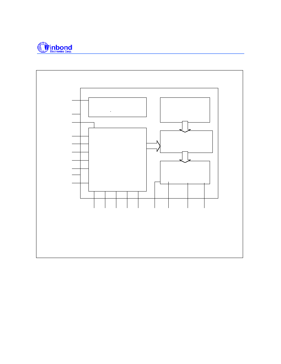
3. BLOCK DIAGRAM
OSC
VDD1
RESET
TEST
TG1
TG2
*TG5
*TG6
VSS1
LED1
*: TG3, TG4 for W523A008 and W523A010
CONTROLLER
ROM
SPEECH
SYNTHESIZER
PWM DRIVER
D/A CONVERTER
TIMING GENERATOR
S
T
P
A
/
B
U
S
Y
S
T
P
B
L
E
D
2
/
S
T
P
C
S
T
P
D
S
T
P
E
V
S
S
2
V
D
D
2
S
P
K
+
/
A
U
D
S
P
K
-

W523AXXX
- 4 -
4. PIN DESCRIPTION
NAME I/O
DESCRIPTION
OSC
I
Ring oscillator input
VDD1
-
Positive power supply
TEST
I
Test pin. Internally pulled low
RESET
I
Active low to reset all devices as POR function. Internally pulled high.
TG1
I
Direct trigger input 1. Internally pulled high
TG2
I
Direct trigger input 2. Internally pulled high
*TG5
I
Direct trigger input 5. Internally pulled high
*TG6
I
Direct trigger input 6. Internally pulled high
VSS1
-
Negative power supply
LED1 O
LED1
output
STPA/BUSY
O
Stop signal A or Busy signal
STPB
O
Stop signal B
LED2/STPC
O
LED2 output or Stop signal C
STPD
O
Stop signal D
STPE
O
Stop signal E
SPK- O
PWM
output
AUD/SPK+
O
Current type output or PWM output for speaker
VSS2
-
Negative power supply
VDD2
-
Positive power supply
*: TG3, TG4 for W523A008 and W523A010

W523AXXX
Publication Release Date: May 20, 2003
- 5 -
Revision A3
5. FUNCTIONAL DESCRIPTION
I/O pins:
The W523Axxx family provides up to 4 trigger pins, which can be extended to 24 matrix trigger inputs,
up to 5 STOP output pins and up to 2 LED output pins. All of these I/O pins' status can be easily
defined by PowerSpeech
program.
Powerful programmable features:
The W523Axxx family provides JUMP (JP), LOAD (LD), MOVE (MV), INC, and END commands and
10 programmable registers, such as R0 ~ R3, EN0, EN1, MODE0, MODE1, STOP and PAGE, can be
easily used to program the desired playing mode, stop output signal form, LED flash type, and trigger
pin interrupt modes. The chip's programmable features can also be used to develop new, customized
functions for a wide variety of innovative applications.
Programmable Power-on Initialization:
Whenever the W523Axxx is powered on or pressed the
RESET
pin, the program contained in the
32
nd
voice group will be executed after the power-on delay (about 160 mS), so the user can write a
program into this group to set the power-on initial state. If user does not wish to execute a program at
power-on, an "END" instruction should be entered in the group 32.
The interruption priority is shown as below while other trigger pins as well as JUMP (JP) command are
executing simultaneously during POI executing period:
POI > TG1F > TG1R > TG2F > TG2R > *TG5F > *TG5R > *TG6F > *TG6R > "JP" instruction.
*: TG3, TG4 for W523A008, W523A010
5.1 Register Definition and Control
The register file in the W523Axxx family is composed of 10 registers, including 4 general-purpose
registers and 6 special purpose registers. They are defined to facilitate the operations for various
purposes. The default setting values of the registers are given in the following table.
REGISTER NAME
DEFAULT
SETTING
General Register
R0-R3
00100000B
EN0 (W523A008~A010)
11111111B
EN0 (W523A012~A120)
XX11XX11B
EN1 (W523A012~A120)
XX11XX11B
MODE0, MODE1
11111111B
STOP XXX11111B
Special Register
PAGE 00000000B