W523SXX
(PRELIMINARY)
HIGH FIDELITY
PowerSpeech
TM
Publication Release Date:Oct. 2000
- 1 - Revision A5
GENERAL DESCRIPTION
The W523Sxx family are programmable speech synthesis ICs that utilize Winbond
s new high fidelity
voice synthesis algorithm to generate all types of voice effects with high sound quality.
The W523Sxx' s LOAD, JUMP, MOVE and INC commands and ten programmable registers provide
powerful user-programmable functions that make this chip suitable for an extremely wide range of
speech IC applications.
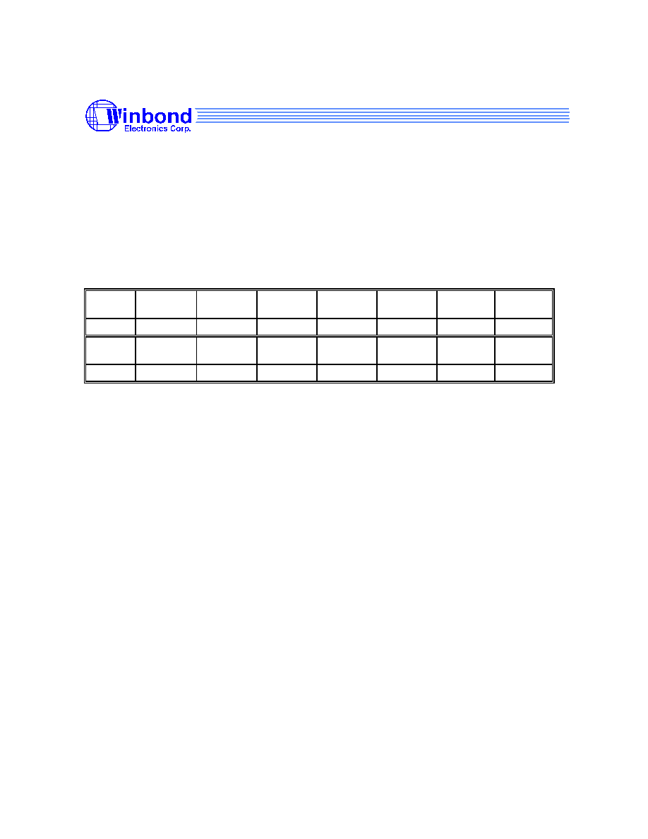
The W523Sxx family includes 14 kinds of bodies which are the same except for the voice duration
shown below:
PART
NO.
W523S08
W523S10
W523S12
W523S15
W523S20
W523S25
W523S30
Duration
8 sec.
10 sec.
12 sec.
15 sec.
20 sec.
25 sec.
30 sec.
PART
NO.
W523S40
W523S50
W523S60
W523S70
W523S80
W523S99
W523M02
Duration
40 sec.
50 sec.
60 sec.
70 sec.
80 sec.
100 sec.
120 sec.
Note: The voice duration is estimated by 6.4 KHz sampling rate.
FEATURES
�
Operating voltage range: 2.4 � 5.5 volts for both DAC and PWM output
�
New high fidelity synthesis algorithm
�
Either PWM mode or D/A converter mode can be selected for AUD output
�
Provides 4 direct trigger inputs that can easily be extended to 24 matrix trigger inputs
�
Two trigger input debounce times (50 mS or 400 uS) can be set
�
Provides up to 2 LEDs and 5 STOP outputs
�
Flexible functions programmable through the following:
-
LD (Load), JP (Jump), MV (Move) and INC (Increase) commands
-
Four general purpose registers: R0, R1, R2 and R3
-
Six special purpose registers: EN0, EN1, MODE0, MODE1, STOP and PAGE
-
Conditional instructions: @LAST, @TGn_HIGH or LOW, where, n = 1,2,5 or 6
-
Speech equations
-
END instruction
�
Supports CPU interface operation
�
Symbolic compiler supported
�
Instruction cycle
400
�
S typically
�
Section control for
-
Variable frequency: 4.8/6/8/12 KHz

W523SXX
(PRELIMINARY)
- 2 -
-
LED: ON/OFF
�
Up to 256 voice groups can be used in single page mode; or extended to 2,048 voice groups
in multi page mode, such as 8-page, 16-page and 32-page.
BLOCK DIAGRAM
OSC
VDD1
RESET
TEST
TG1
TG2
TG5
TG6
VSS1
LED1
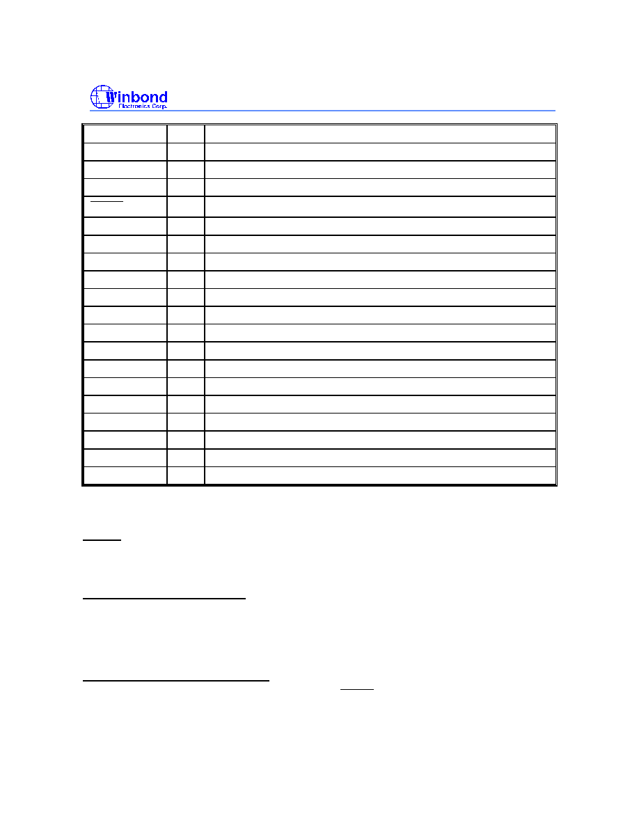
PIN DESCRIPTION
CONTROLLER
ROM
SPEECH
SYNTHESIZER
PWM DRIVER
D/A CONVERTER
TIMING GENERATOR
STPA/BUSY
STPB
LED2/STPC
STPD
STPE
VSS2
VDD2
SPK+/AUD
SPK
-
W523SXX
(PRELIMINARY)
Publication Release Date: Oct 2000
- 3 - Revision A5
NAME
I/O
DESCRIPTION
OSC
I
Ring oscillator input
VDD1
-
Positive power supply
TEST
I
Test pin. Internally pulled low
RESET
I
Active low to reset all devices as POR function. Internally pulled high.
TG1
I
Direct trigger input 1. Internally pulled high
TG2
I
Direct trigger input 2. Internally pulled high
TG5
I
Direct trigger input 5. Internally pulled high
TG6
I
Direct trigger input 6. Internally pulled high
VSS1
-
Negative power supply
LED1
O
LED1 output
STPA/BUSY
O
Stop signal A or Busy signal
STPB
O
Stop signal B
LED2/STPC
O
LED2 output or Stop signal C
STPD
O
Stop signal D
STPE
O
Stop signal E
SPK-
O
PWM output
AUD/SPK+
O
Current type output or PWM output for speaker
VSS2
-
Negative power supply
VDD2
-
Positive power supply
FUNCTIONAL DESCRIPTION
I/O pins:
The W523Sxx family provides up to 4 trigger pins, which can be extended to 24 matrix trigger inputs,
up to 5 STOP output pins and up to 2 LED output pins. All of these I/O pins' status can be easily
defined by PowerSpeech
TM
program.
Powerful programmable features:
The W523Sxx family provides JUMP (JP), LOAD (LD), MOVE (MV), INC, and END commands and 10
programmable registers, such as R0 ~ R3, EN0, EN1, MODE0, MODE1, STOP and PAGE, can be
easily used to program the desired playing mode, stop output signal form, LED flash type, and trigger
pin interrupt modes. The chip' s programmable features can also be used to develop new, customized
functions for a wide variety of innovative applications.
Programmable Power-on Initialization:
Whenever the W523Sxx is powered on or pressed the RESET pin, the program contained in the 32
nd
voice group will be executed after the power-on delay (about 160 mS), so the user can write a
program into this group to set the power-on initial state. If user does not wish to execute a program at
W523SXX
(PRELIMINARY)
- 4 -
power-on, an " END" instruction should be entered in the group 32.
The interruption priority is shown as below while other trigger pins as well as JUMP (JP) command are
executing simultaneously during POI executing period:
POI > TG1F > TG1R > TG2F > TG2R > TG5F > TG5R > TG6F > TG6R > "JP" instruction.
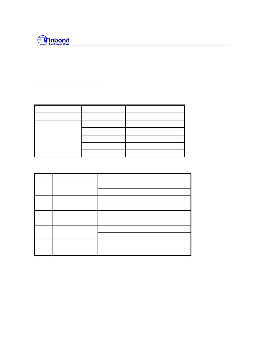
Register Definition and Control
The register file in the W523Sxx family is composed of 10 registers, including 4 general-purpose
registers and 6 special purpose registers. They are defined to facilitate the operations for various
purposes. The default setting values of the registers are given in the following table.
REGISTER
NAME
DEFAULT SETTING
General Register
R0-R3
00100000B
EN0
XX11XX11B
EN1
XX11XX11B
MODE0, MODE1
11111111B
STOP
XXX11111B
Special Register
PAGE
00000000B
1. MODE0 Register
BIT
DESCRIPTION
DEFINITION
1: Flash
7
LED mode
0: DC
1: LED2 output
6
LED2/STPC
pin selection
0: STPC output
1: Long
4
Debounce time
0: Short
1: STPA output
2
STPA/BUSY
pin selection
0: BUSY output
5,3,1,0 X
Don' t care
The MODE0.7 bit defines the output type of LED1 and LED2 pins as Flash output (3 Hz) or DC output.
The MODE0.6 bit defines the configuration of LED2/STPC pin' s status as LED2 output or STPC
output. The MODE0.4 bit defines the trigger pin' s debounce time as long debounce (50 mS) or short
debounce (400 uS). The MODE0.2 bit defines the behavior of the STPA/BUSY pin as STPA output in
normal mode or BUSY signal output in CPU mode. The bits 5, 3, 1 and 0 are don' t care bits.

W523SXX
(PRELIMINARY)
Publication Release Date: Oct 2000
- 5 - Revision A5
2. MODE1 Register
BIT
DESCRIPTION
DEFINITION
7, 6, 1, 0
X
Don' t care
1: Alternate
5
LED Flash type
0: Synchronous
1: YES
4
LED1 section
control
0: NO
1: SECTION control
3
LED2 control
0: STPC control
1: OFF
2
LED1 volume
control
0: ON
MODE1.5 is for LED flash type control. MODE1.4 is for LED1 section control ON/OFF. MODE1.3 is for
LED2 Section/STPC control. MODE1.2 is for LED1 volume control.
3. PAGE Register
BIT
7
6
5
4
3
2
1
0
PAGE
-
-
-
PG4
PG3
PG2
PG1
PG0
The bits 0 ~ 4 in PAGE register are used for page selection. Once the page mode being defined
(referring to the below section of "Option Control Function"), the working page is selected by the bits 0
~ 4 in the PAGE register. Hence, the user can execute "LD PAGE, value" instruction to change the
working page of the voice entry group. Not all of the bits 0 ~ 4 of PAGE register are used in different
page mode. They are listed as below table:
PAGE MODE
PG4
PG3
PG2
PG1
PG0
1-page
�
�
�
�
�
8-page
�
�
16-page
�
32-page
Where "
�
" means don
t care and "
" means must be set properly.
4. EN Register
BIT
7
6
5
4
3
2
1
0
EN0
X
X
TG2R
TG1R
X
X
TG2F
TG1F
EN1
X
X
TG6R
TG5R
X
X
TG6F
TG5F
EN0 or EN1 is an 8-bit register that stores the rising/falling edge enable or disable status information
for all trigger pins, which determines whether each trigger pin is retriggerable, non-retriggerable,
W523SXX
(PRELIMINARY)
- 6 -
overwrite, or non-overwrite. The 8-bit structure of this register and the rising or falling edge of the
triggers corresponding to each bit are shown above. " X" indicates a " don' t care" bit.
The TG1, 2, 5, 6 represents triggers 1, 2, 5 and 6 respectively; the "R" represents the rising edge; and
"F" represents the falling edge. When any one of the eight bits is set to "1", the rising or falling edge of
the corresponding trigger pin can be enabled, interrupting the current state.
5. STOP Register
BIT
7
6
5
4
3
2
1
0
STOP
X
X
X
STE
STD
STC
STB
STA
The STOP register stores stop output status information to determine the voltage level of each stop
output pin. The 8-bit structure of this register and the stop output pin corresponding to each bit are
show as above table. The "X" indicates a "don' t care" bit. When a particular STOP bit is set to "1", the
corresponding stop signal will be an active high output.
6. R0-R3 Registers
These four registers are 8-bit register that stores the entry values of from 0 to 255 voice groups. R0 is
a special register that can be incremented by "INC" instruction.
Option Control Function
There are four types of option control in W523Sxx. They can be determined by a declaration in the
user
s program file, but cannot be controlled by register.
FUNCTION
MASK OPTION
DECLARATION
DEFINITION
DEFPAGE 1
256 interrupt vector/label for 1 page, 1 page in total (1-page mode)
DEFPAGE 8
256 interrupt vector/label for 1 page, 8 pages in total (8-page mode)
DEFPAGE 16
128 interrupt vector/label for 1 page, 16 pages in total (16-page mode)
Page mode
configuration
DEFPAGE 32
64 interrupt vector/label for 1 page, 32 pages in total (32-page mode)
NORMAL
Normal mode operation
Operation
mode
CPU
CPU mode operation
OSC_3MHz
3 MHz oscillator
Oscillator
frequency
OSC_1.5MHz
1.5 MHz oscillator
VOUT_DAC
DAC (AUD) output
Voice
output type
VOUT_PWM
PWM output
"DEFPAGE" determines the page operation mode in W523Sxx. The default setting of the page mode
is 1-page mode. The 8-page, 16-page or 32-page mode can be declared to extend the voice group
entry from 256 to 2047 in PowerSpeech
TM
program.
The W523Sxx can communicate with an external microprocessor through the simple serial CPU
interface, which is the same as the W583xx series. The CPU interface consists of the TG1, TG2, and
STPA/BUSY pins. "NORMAL" and "CPU" decide whether the operation mode of W523Sxx will be
normal mode or CPU mode.
"OSC_3MHz" and "OSC_1.5MHz" select the frequency of the system clock. "VOUT_DAC" and
"VOUT_PWM" select the voice output type.
W523SXX
(PRELIMINARY)
Publication Release Date: Oct 2000
- 7 - Revision A5
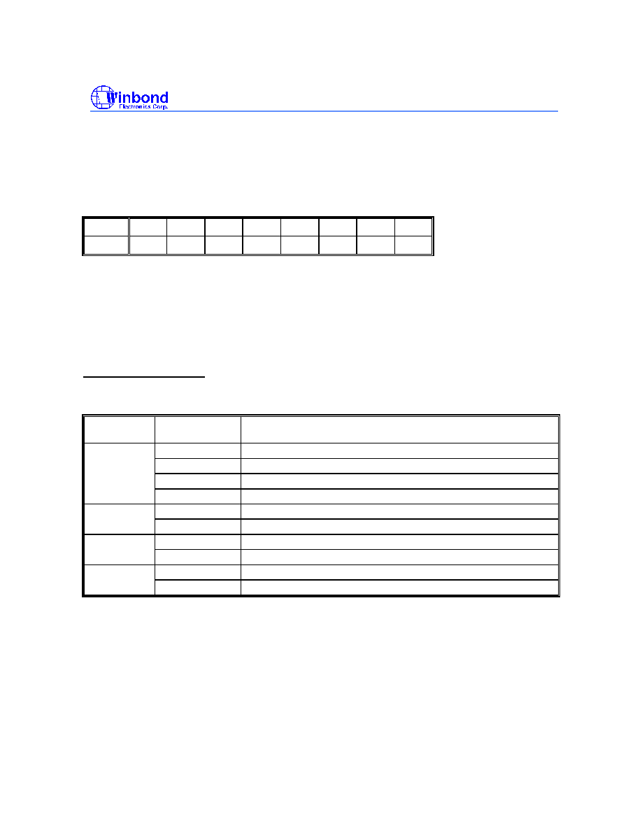
Interrupt Vector Allocation
The W523Sxx provides a total of 4 trigger inputs to communicate with the outside world. Each trigger
pin can invoke 2 dedicate interrupt vectors depending on TG pins' status (rising or falling). The table
below shows the relationship between triggers' status and interrupt vectors.
INTERRUPT VECTOR
TRIGGER SOURCE
0
TG1F
1
TG2F
8
TG5F
9
TG6F
INTERRUPT VECTOR
TRIGGER SOURCE
4
TG1R
5
TG2R
12
TG5R
13
TG6R
32
POI
CPU Interface
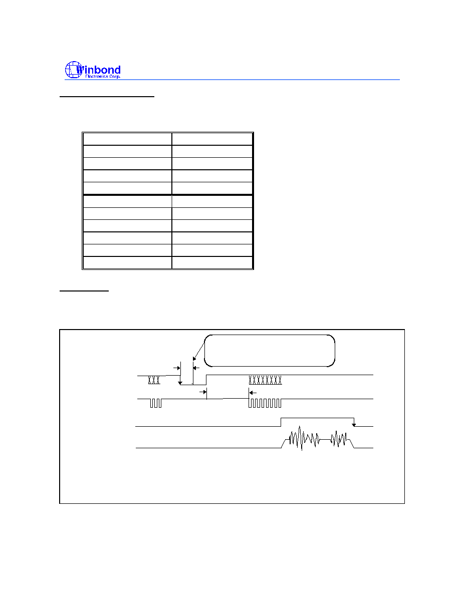
The W523Sxx can communicate with an external microprocessor through a simple serial CPU
interface. The CPU interface consists of TG1, TG2 and STPA/BUSY pins, which are shown below:
Debounced OK. to clear the internal CPU
counter for preventing the system from
running away. (TG1F should be disabled.)
T
DEB
END
T
CRD
TG1
(Data)
TG2
(Clock)
STPA/Busy
AUD/SPK+
Note:
1. T
DEB
means the "Debounce time".
2. T
CRD
is the "CPU Reset Delay" time. This should be more than 2.6
�
S.
3. The "Clock" frequency of the TG2 pin can be set in the range: 10 KHz - 1 MHz.
Busy signal will output "high" after the end of transmission. The rising timing of Busy signal is
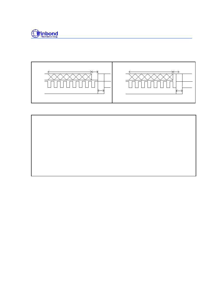
W523SXX
(PRELIMINARY)
- 8 -
dependent on the MSB of data output on TG1 (Data) pin. If MSB is "1", Busy will rise after the last
rising edge of TG2 (Clock) pin. If MSB is "0", Busy will rise after the rising edge that TG1 (Data)
returns to high.
TG1
(DATA)
TG2
(CLK)
BUSY
7 bits
MSB=0
40ns
TG1
(DATA)
TG2
(CLK)
BUSY
7 bits
MSB=1
40ns
To place the W523Sxx in CPU mode, program the code according to the following example.
W523S15
CPU ; Reserved word, used as a directive to notify the compiler for post processing.
LED1
FREQ2
POI:
LD MODE0,XX1XX0XXB ;bit2=0 BUSY
LD EN0, 0x00
H5+voice1+T5
END
34: ; Direct trigger or CPU interrupt.
H5+voice2+T5
END
The defaulted operating mode in W523Sxx is normal mode (or manual trigger mode), which is
identified by the "Normal" and "CPU" option control. To enter the CPU mode, the "CPU" declaration
must be inserted in the declaration region of program (*.out). In CPU mode, the bit MODE0.2, which is
defined as STPA or BUSY selection for the STPA/BUSY pin, will be selected as "0" (BUSY output)
automatically by the compiler unless otherwise specified explicitly by the STPA directive. The CPU,
STPA, and BUSY directives can appear only in the first paragraph of the *.out files so that the
compiler will automatically interpret them as Stop definitions in the POI interrupt vector. If these
directives are placed elsewhere, an error message will be issued during the compilation process.
In the program example shown above, the external
�
C will transfer one byte data "34" to W523Sxx.
The number 34 (Decimal) is equal to 00100010b (Binary). The interface timing is shown below.
W523SXX
(PRELIMINARY)
Publication Release Date: Oct 2000
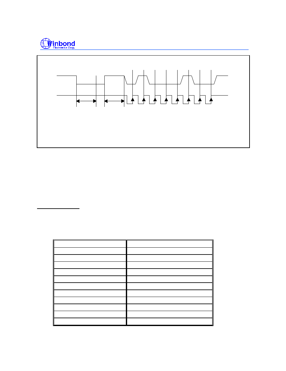
- 9 - Revision A5
TG1
TG2
(Data)
(Clock)
0
1
0
0
0
1
0
0
MSB
LSB
<1>
<2>
<3>
<4>
DEB
T
CRD
T
<1> When TG1 is pulled low, the W523Sxx stops playing voice or executing instruction and waits for data from
the external
�
C.
<2> If TG1 is debounced OK, the W523Sxx will clear the CPU receiving buffer.
<3> 8-bit data are transferred by TG1 (Data) and TG2 (Clock). LSB is sent firstly.
<4> TG1 returns to high and starts the CPU interrupt service. In this case W523S15 will play the
H51+voice2+T51 sections and the STPA/BUSY pin is pulled high during the playing period.
The TG1 pin, which is pulled high with a 500K
resistor, should be kept high during non-transmission
periods to reduce power consumption. The external
�
C should be connected to the W523Sxx by an
inverted-type output port for better noise immunity. In CPU mode, the W523Sxx stops operating upon
the falling edge of the TG1 pin. For the CPU interface to work normally, TG1F should be disabled.
Thus, one suggestion is that TG1F, TG1R, TG2F, and TG2R should all be disabled in CPU mode. The
master frequency of the external
�
C, and hence the clock rate of TG1 and TG2, tends to vary among
different vendors and applications.
Note: In CPU mode application, in case the last voice group entry point, 255, is no used, it should be
typed " END" command to avoid abnormal operating.
Instruction Set List
There are two types of instruction in the W523Sxx, unconditional and conditional instructions. The first
types of instructions are executed immediately after they are issued. The second types of instructions
are executed only when the conditions specified in the instruction are satisfied. All the instructions are
listed in the following table. The cycle time for each instruction is 2/Sampling Frequency (Fs). For
example, Fs = 6.0 KHz, the cycle time is 333
�
S.
UNCONDITIONAL
CONDITIONAL
JP
G
JP
G
@STS
JP
Rn
JP
Rn
@STS
LD
EN0, value
LD
EN0, value
@STS
LD
EN1, value
LD
EN1, value
@STS
LD
MODEi, value
LD
MODEi, value
@STS
LD
STOP, value
LD
STOP, value
@STS
LD
PAGE, value
LD
PAGE, value
@STS
LD
Rn, value
LD
Rn, value
@STS
END
END
@STS
MV
Rn, Rm
MV
Rn, Rm
@STS
INC
INC
@STS

W523SXX
(PRELIMINARY)
- 10 -
Legend:
G: Interrupt vector/label
Rn: R0-R3
Rm: R0-R3
MODEi: MODE0, MODE1
value: 8-bit data
@STS can be the following: @LAST, @TGn_HIGH, @TGn_LOW, n = 1
-
4.
ABSOLUTE MAXIMUM RATINGS
PARAMETER
SYMBOL
CONDITIONS
RATED VALUE
UNIT
Power Supply
V
DD
-
V
SS
-
-0.3 to +7.0
V
Input Voltage
V
IN
All Inputs
V
SS
-0.3 to V
DD
+0.3
V
Storage Temp.
T
STG
-
-55 to +150
�
C
Operating Temp.
T
OPR
-
0 to +70
�
C
Note: Exposure to conditions beyond those listed under Absolute Maximum Ratings may adversely affect the life and reliability
of the device.
ELECTRICAL CHARACTERISTICS
(T
A
= 25
�
C, V
SS
= 0V)
DC CHARACTERISTICS
PARAMETER
SYM.
CONDITIONS
MIN.
TYP.
MAX.
UNIT
DAC output
2.4
3.0
5.5
V
Operating Voltage
V
DD
PWM output
2.4
3.0
5.5
V
V
IL
V
SS
�0.3
-
0.3
�
V
DD
V
Input Voltage
V
IH
0.7
�
V
DD
-
V
DD
I
SB1
V
DD
= 3V, All I/O pins
unconnected, No Playing
1
�
A
Standby Current
I
SB2
V
DD
= 5V, All I/O pins
unconnected, No Playing
1
�
A
I
OP1
V
DD
= 3V, No Load
500
�
A
Operating Current
(Ring type)
I
OP2
V
DD
= 5V, No Load
1
mA
Input Current of
TG1-TG4 pins
I
IN1
V
DD
= 3V, Vin = 0V
-8
�
A
Input Current of
TEST pin
I
IN2
V
DD
= 3V, Vin = 3V
30
�
A
Input Current of
SEL, RESET
I
IN3
V
DD
= 3V, Vin = 0V
-8
�
A
SPK (D/A Full
Scale)
I
DAC
V
DD
= 4.5V, Rl = 100
-4.0
-5.0
-6.0
mA
W523SXX
(PRELIMINARY)
Publication Release Date: Oct 2000
- 11 - Revision A5
I
OL1
V
DD
= 3V, Vout = 0.4V
0.8
mA
Output Current of
STPA-STPE
I
OH1
V
DD
= 3V, Vout = 2.7V
-0.8
mA
I
OL2
100
mA
Output Current of
SPK+, SPK-
I
OH2
V
DD
= 3V, Rl = 8
-100
mA
AC CHARACTERISTICS
PARAMETER
SYM.
CONDITIONS
MIN. TYP. MAX. UNIT
Ring oscillator, Rosc = 270 K
2.7
3
3.3
MHz
Oscillation Frequency
(W58300 ICE chip)
Fosc1
Ring oscillator, Rosc = 560 K
1.3
1.5
1.7
MHz
Ring Oscillator, Rosc = 1.2 M
2.7
3
3.3
MHz
Oscillation Frequency
(W523Sxx production
chip)
Fosc2
Ring Oscillator, Rosc = 2.4 M
1.3
1.5
1.7
MHz
Oscillation Frequency
Deviation by Voltage
Drop
Fosc2
Fosc2
F(3V)-F(2.4V)
F(3V)
7.5
%
Instruction Cycle Time
Tins
Fosc = 3 MHz, SR = 6 KHz
1/3
mS
POI Delay Time
T
PD
Fosc = 3 MHz
160
mS
Long Debounce Time
T
DEBL
50
mS
Short Debounce Time
T
DEBS
Fosc = 3 MHz, SR = 6 KHz
400
�
S
BONDING PAD DIAGRAM
19
1
2
3
4 5 6 7 8 9 10 11 12 13 14 15 16 17 18
W523SXX
(PRELIMINARY)
- 12 -
PAD NO.
PAD NAME
PAD NO.
PAD NAME
1
VDD1
12
LED2/STPC
2
RESET
13
STPD
3
TEST
14
STPE
4
TG1
15
VSS2
5
TG2
16
VDD2
6
TG5
17
SPK-
7
TG6
18
AUD/SPK+
8
VSS1
19
OSC
9
LED1
10
STPA/BUSY
11
STPB
TYPICAL APPLICATION CIRCUIT
1. DAC output:
Note:
1. In principle, the playing speed determined by Rosc should correspond to the sampling rate during the coding phase. The
playing speed may be adjusted by varing Rosc, however.
VDD (1.8V ~ 5.5V)
TG1
TG2
TG5
TG6
/RESET
VDD2
VDD1
TEST
LED1
OSC
STPA/BUSY
STPB
VSS2
VSS1
LED2/STPC
STPD
STPE
AUD/SPK+
SPK-
Rosc
Rs
Cs
NPN T'x
Speaker
8 ohm
� watt
LED
100 ohm
LED
100 ohm
W523Sxx
W523SXX
(PRELIMINARY)
Publication Release Date: Oct 2000
- 13 - Revision A5
2. Rs is an optional current-dividing resistor. If Rs is added, the resistance should be between 390 and 820 ohm.
3. The typical Rosc = 1.2 Mohm for 3 MHz Fosc; and Rosc = 2.4 Mohm for 1.5 MHz Fosc.
4. Cs is optional.
5. The DC current gain of the NPN transistor ranges from 120 to 200.
6. All unused trigger pins can be left open because of their internal pull-high resistance.
7. The OSC layout in customer's PCB should be as closed as the OSC pad to avoid noise coupling.
8. The chip's substrate must be wired to Vss.
2. PWM output:
Note:
1. In principle, the playing speed determined by Rosc should correspond to the sampling rate during the coding phase. The
playing speed may be adjusted by varing Rosc, however.
2. The typical Rosc = 1.2 Mohm for 3 MHz Fosc; and Rosc = 2.4 Mohm for 1.5 MHz Fosc.
3. The capacity, 10 uF, is necessary to reduce voltage fluctuation while PWM outputting.
4. All unused trigger pins can be left open because of their internal pull-high resistance.
5. The OSC layout in customer's PCB should be as closed as the OSC pad to avoid noise coupling.
6. The chip's substrate must be wired to Vss.
VDD (2.4V ~ 5.5V)
TG1
TG2
TG5
TG6
/RESET
VDD2
VDD1
TEST
LED1
OSC
STPA/BUSY
STPB
VSS2
VSS1
LED2/STPC
STPD
STPE
AUD/SPK+
SPK-
Rosc
Speaker
8 ohm
� watt
LED
100 ohm
LED
100 ohm
W523Sxx
10 uF

W523SXX
(PRELIMINARY)
- 14 -
Revision History in W523SXX Data Sheet
Version Date
Editor
Description
A1
May-1-2000
Steven Lin
Initial Issued
A2
May-19-2000
Steven Lin
1. Add DAC and PWM application circuits.
2. Add PWM voltage as 2.4V ~ 5.5V in DC characteristic
table.
A3
Jul-3-2000
Steven Lin
1. GENERAL DESCRIPTION, 3
rd
line: " ...and INC
commands and ten programmable registers provide ...
"
2. FEATURE, 1st line: 1.8 - 5.5 Volts for DAC output and
2.4 � 5.5 Volts for PWM output.
3. FEATURE, 4
th
line: "New high fidelity synthesis algorithm"
It' s deleted for redundant.
4. FEATURE, last line: "Up to 256 voice groups can be used
in single page mode; or extended to 2,048 voice groups
in multi page mode, such as 8-page, 16-page and
32-page."
5. FUNCTION DESCRIPTION: Modified the description for
more easy readable.
6. STOP Register: When a particular STOP bit is set to "1",
the corresponding stop signal will be an active high
output.
7. Add CPU interface description in timing diagram,
operation and notified.
8. APPLICATION CIRCUIT: Add a note in number 7, "The
OSC layout on customer' s PCB should be as closed as
the OSC pad to avoid noise coupling." for both of DAC
and PWM output application circuit.
A4
Jul-25-2000
Steven Lin
1. APPLICATION CIRCUIT in PWM output diagram: Add a
capacity, 10 uF, between VDD and GND to reduce
voltage fluctuation while PWM outputting.
A5
Oct-25-2000
Steven Lin
1. FEATURE, 1
st
line: Operating voltage 2.4 ~ 5.5 volts for
both DAC and PWM output.
2. DC spec., DAC voltage: minimum 2.4V.
Headquarters
No. 4, Creation Rd. III,
Science-Based Industrial Park,
Hsinchu, Taiwan
TEL: 886-3-5770066
FAX: 886-3-5792697
http://www.winbond.com.tw/
Voice & Fax-on-demand: 886-2-27197006
Taipei Office
11F, No. 115, Sec. 3, Min-Sheng East Rd.,
Taipei, Taiwan
TEL: 886-2-27190505
FAX: 886-2-27197502
Winbond Electronics (H.K.) Ltd.
Rm. 803, World Trade Square, Tower II,
123 Hoi Bun Rd., Kwun Tong,
Kowloon, Hong Kong
TEL: 852-27513100
FAX: 852-27552064
Winbond Electronics North America Corp.
Winbond Memory Lab.
Winbond Microelectronics Corp.
Winbond Systems Lab.
2727 N. First Street, San Jose,
CA 95134, U.S.A.
TEL: 408-9436666
FAX: 408-5441798
Note: All data and specifications are subject to change without notice.