W528SXX
ADPCM VOICE SYNTHESIZER
(PowerSpeech)
Publication Release Date: Nov 2000
- 1 - Revision A1
GENERAL DESCRIPTION
The W528xxx family are programmable speech synthesis ICs that utilize the ADPCM coding method to
generate all types of voice effects.
The W528xxx's LOAD and JUMP commands and four programmable registers provide powerful user-
programmable functions that make this chip suitable for an extremely wide range of speech IC
applications.
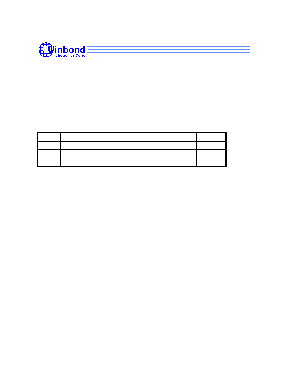
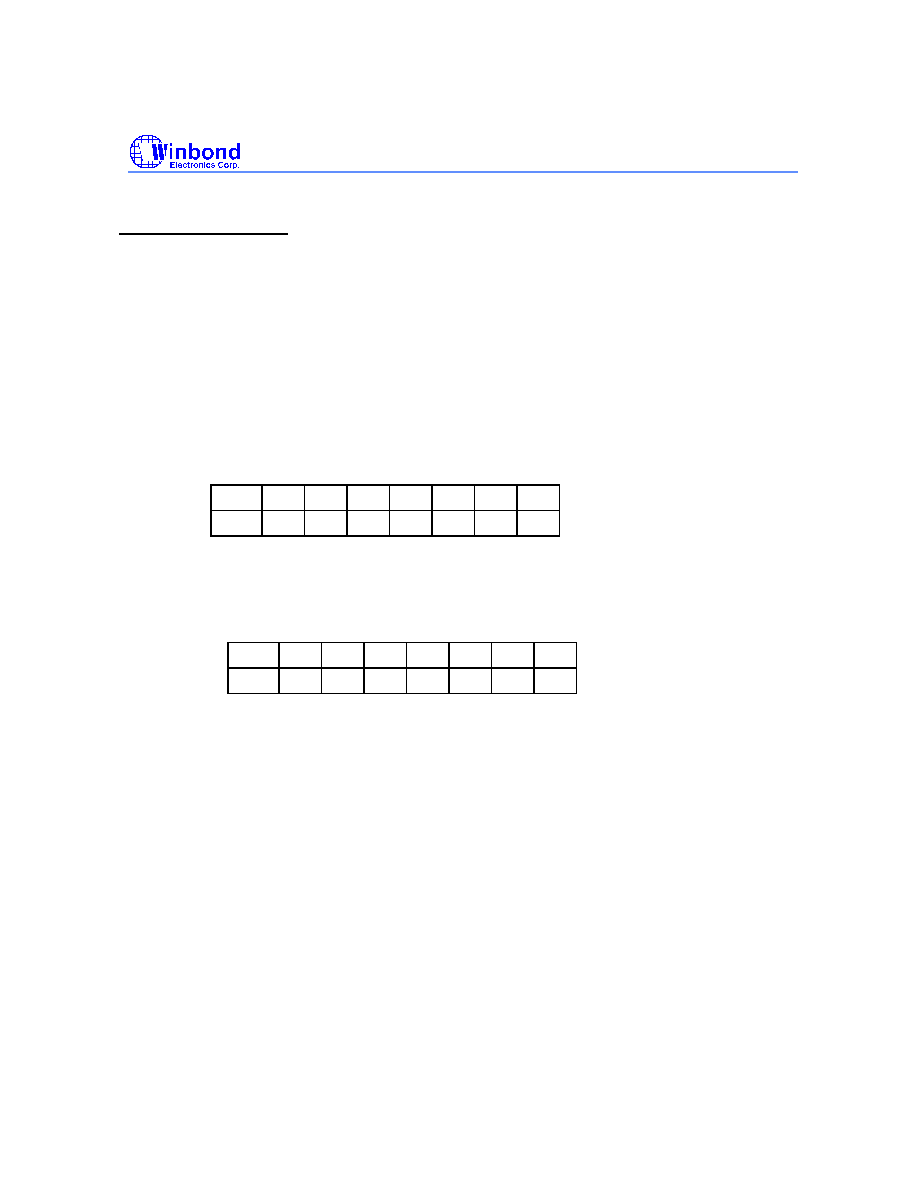
The W528xxx family includes 12 kinds of bodies which are the same except for the voice duration
shown below:
BODY
W528S03 W528S05 W528S08A W528S10 W528S12
W528S15
Second
3 Sec
5 Sec
8 Sec
10 Sec
12 Sec
15 Sec
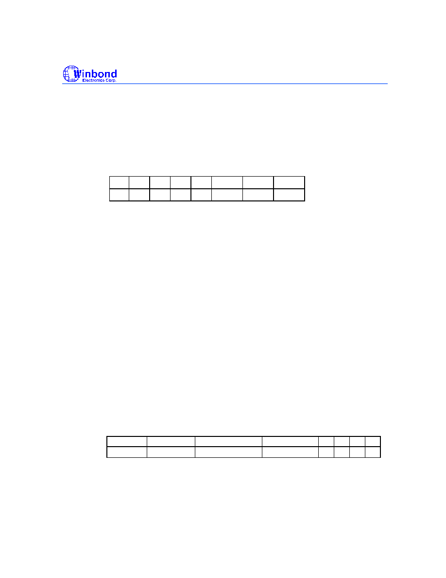
BODY
W528S20 W528S25
W528S30
W528S40 W528S50
W528S60
Second
20 Sec
25 Sec
30 Sec
40 Sec
50 Sec
60 Sec
Note: The voice durations are estimated by 6.4KHz sampling rate.
FEATURES
�
Programmable speech synthesizer
�
Wide operating voltage range: 2.4 to 5.5 volts
�
4-bit ADPCM synthesis method
�
Provides 4 direct trigger inputs that can easily be extended to 8 or 12 matrix trigger inputs
�
Two trigger input debounce times (20 to 40 mS or 160 to 320
�
S) can be set
�
Provides up to 2 LEDs and 3 STOP outputs
�
Every LED pin can drive 3 LEDs simultaneously
�
LED flash frequency: 3 Hz
�
AUD output current: 5 mA
�
Flexible functions programmable through the following:
-
LD (load), JP (jump) commands
-
Four registers: R0, EN, STOP, and MODE
-
Conditional instructions
-
Speech equation
-
END instruction
-
Global repeat (GR) setting
-
Output frequency and LED flash type setting
�
Programmable power-on initialization (POI) (can be interrupted by trigger inputs)
W528SXX
- 2 -
�
POI delay time of 160 mS ensures stable voltage when chip is powered on
�
Can be programmed for the following functions:
-
Interrupt or non-interrupt for rising or falling edge of each trigger pin (this feature determines
retriggerable, non-retriggerable, overwrite, and non-overwrite features of each trigger pin)
-
Four playing modes:
One Shot (OS)
Level Hold (LH)
Single-cycle level hold (S_LH)
Complete-cycle level hold (C_LH)
-
Stop output signal setting
-
Serial, direct, or random trigger mode setting
�
Four frequency options (4/4.8/6/8 KHz) and LED On/Off control can be set independently in each
GO instruction of speech equation
�
Independent control of LED1 and LED2
�
Total of 256 voice group entries available for programming
�
Provides the following mask options:
-
LED flash type: synchronous/alternate
-
LED1 section-controlled: Yes/No
-
LED2: section-controlled/STPC-controlled
-
LED volume-controlled: No/Yes
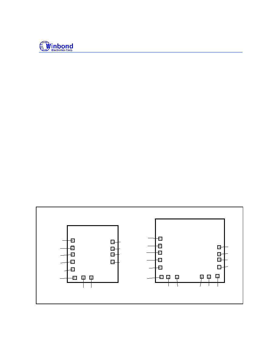
PAD CONFIGURATIONS
TG4/LED2/STPC
W5285-9
W5281-4
TEST
TG1
TG2
TG3
LED1
STPB
STPA
SPK
V
V
OSC
TEST4
TG1
TG2
TG3
TG4/LED2/STPC
LED1
STPB
STPA
SPK
TEST1 TEST2
V
V
OSC
TEST3
DD
SS
DD
SS
W528S03-S12
W528S15-S60
W528SXX
Publication Release Date: Nov 2000
- 3 - Revision A1
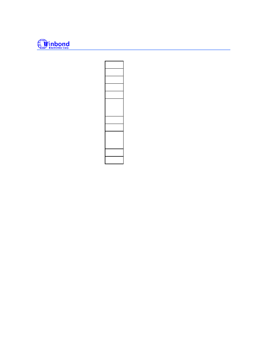
PAD DESCRIPTION
PAD NAME
I/O
FUNCTION
TG1
I
Trigger Input 1
TG2
I
Trigger Input 2
TG3
I
Trigger Input 3
TG4/LED2/STPC
I/O
Trigger Input 4 or LED 2 or Stop Signal C
LED1
O
LED 1
STPB
O
Stop Signal B
STPA
O
Stop Signal A
SPK
O
Current Output for Speaker
V
SS
-
Negative Power Supply
V
DD
-
Positive Power Supply
OSC
I
Oscillation Frequency Control
*Test1
-
Test Pin
*Test2
-
Test Pin
*Test3
-
Test Pin
Test4
-
Test Pin
* These pads only exist in W528S15~60.
W528SXX
- 4 -
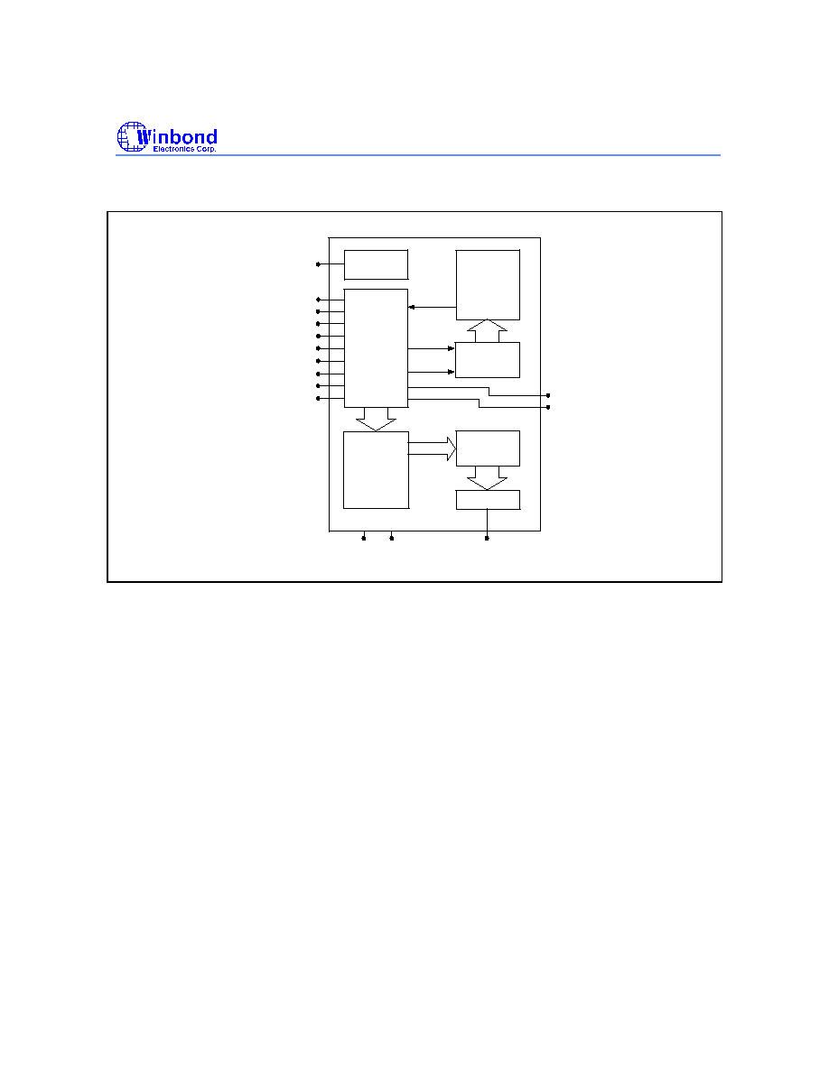
BLOCK DIAGRAM
OSC
TIMING
GENERATOR
DATA ROM
TG1
TG2
TG3
LED1
TG4/LED2/STPC
CONTROLLER
COUNTER
REGISTER
STPA
STPB
SYNTHESIZER
ADPCM
CONVERTER
REGISTER
SPK
& SHIFT
SHIFT
D/A
V
V
*TEST1
DD
SS
*TEST2
*TEST3
TEST4
* These pins only exist in W528S15~60.
FUNCTIONAL DESCRIPTION
The W528Sxx family provides up to four direct trigger pins, which can be extended to eight or twelve
matrix trigger inputs, up to three stop signal output pins, an LED section control, and powerful
programmable features. The JUMP and LOAD commands and four programmable registers can be
used to program the desired playing mode, stop output signal form, LED flash type, and trigger pin
interrupt modes.
The chip's programmable features can also be used to develop new, customized functions for a wide
variety of innovative applications.
A. Instruction Set Description
This section describes three types of instructions:
�
Unconditional instructions, which are executed immediately after they are issued.
�
Conditional instructions, which are executed only when the conditions specified in the instructions
are satisfied.
�
END instruction, which is used to stop all device activity.
Instructions are programmed by writing LOAD and JUMP commands into the R0, EN, STOP, and
MODE registers.
W528SXX
Publication Release Date: Nov 2000
- 5 - Revision A1
Unconditional Instructions:
1. LOAD (LD) Command:
LD R0, value:
This instruction is used to load a voice-group entry value into register R0. The voice-group entry value
may range from 0 to 255. The initial value of the R0 register is "00000000."
LD EN, operand:
This instruction is used to define the trigger interrupt settings by loading the operand message into
register EN. The initial value of the EN register is "11111111."
a. The operand is an 8-bit value that can be entered in decimal (default) or hexadecimal
(with "0x" as a prefix).
b. EN is an 8-bit register that is used to enable/disable the rising/falling edge of each of the four
trigger inputs.
The 8 bits correspond to the rising/falling edges of the triggers as shown below:
Bit:
7
6
5
4
3
2
1
0
TG:
4R
3R
2R
1R
4F
3F
2F
1F
where "nR/F" represents the rising/falling edge of the n-th trigger pin.
c. When any one of the eight bits is set to "1" (default), the corresponding trigger will interrupt the
current state at the edge indicated. When the bits are set to "0," the triggers will be disabled.
d. The voice group entry addresses correspond to the interrupt vectors as follows:
TG:
4R
3R
2R
1R
4F
3F
2F
1F
Group:
7
6
5
4
3
2
1
0
EXAMPLE:
The instruction "LD EN, 0x41" is programmed.
EXPLANATION:
a. "41" is a hexadecimal value equal to the binary value "0100 0001."
b. These 8 bits of data represent the following trigger interrupt settings:
4R,
3R,
2R,
1R,
4F,
3F,
2F,
1F
0
1
0
0
0
0
0
1
RESULT:
a. When the rising edge of TG3 (3R) is activated, the EN register will cause TG3 to interrupt the
current playing state and jump immediately to voice group 6, the voice group that corresponds
to 3R.
b. When the falling edge of TG1 goes active, the EN register will cause TG1 to interrupt the current
playing state and jump immediately to voice group 0, the voice group that corresponds to 1F.
W528SXX
- 6 -
c. No action will be taken when the other trigger pins are pressed, because the corresponding bits
are set to "0."
LD STOP, operand:
This instruction loads the operand message into the STOP register to set the output levels of the stop
signals. The initial value of the STOP register is "XXXXX111."
a. This register is used to program the output levels of the three STOP signals, STPA, STPB,
and STPC. Only three of the bits in the register are used, as shown below (an "X" indicates
"Don't care"):
Bit:
7
6
5
4
3
2
1
0
Stop:
X
X
X
X
X
STPC
STPB
STPA
b. When a particular STOP bit is set to "1," The corresponding stop signal will be a high output;
when a bit is set to "0," the corresponding stop signal will be a low output.
EXAMPLE:
The instruction "LD STOP, 0x43" is programmed.
EXPLANATION:
a. "43" is a hexadecimal value equal to a binary value of "0100 0011."
b. These 8 bits of data represent the following settings:
X,
X,
X,
X,
X,
STPC,
STPB,
STPA
0
1
0
0
0
0
1
1
RESULT:
a. The STPA and STPB outputs will be high outputs.
b. The STPC signal will be a low output.
c. The sixth bit "1" is a "Don't Care" bit and so has no effect on the stop signal output
settings.
LD MODE, operand:
This instruction is used to select various operating modes. It loads an operand message into the
MODE register to select one mode from each of four pairs of modes, which correspond to bits 4
through 7 of the register (bits 0 to 3 are "Don't Care" bits). The four pairs of modes and the
corresponding bits are as follows:
Bit:
7
6
5
4
3
2
1
0
MODE: Flash/DC LED2/STPC TG4/LED2_STPC 45 mS/350
�
S
X
X
X
X
A "1" for one of these bits selects the first of the pair of modes indicated; a "0" selects the second of
the pair. The initial value of the mode register is "1111XXXX."

W528SXX
Publication Release Date: Nov 2000
- 7 - Revision A1
EXAMPLE 1:
The four bits are programmed as "1111," so that the eight bits of the register are as follows (an "X"
indicates a "Don't Care" bit):
Flash/DC, LED2/STPC, TG4/LED2_STPC, 45 mS/350
�
S,
X,
X,
X,
X
1
1
1
1
X
X
X
X
RESULT:
The mode settings are as follows:
a. Pin 4 (TG4/LED2_STPC) is configured as a trigger pin (TG4), and the LED2/STPC option will
be ignored.
b. The LED is set as a flash type, with a flash frequency of 3 Hz.
c. The debounce time of the trigger inputs is set to 45 mS.
EXAMPLE 2:
The four bits are programmed as "0000," so that the eight bits of the register are as follows (an "X"
indicates a "Don't Care" bit):
Flash/DC, LED2/STPC, TG4/LED2_STPC, 45 mS/350
�
S,
X,
X, X,
X
0
0
0
0
X
X
X
X
RESULT:
The mode settings are as follows:
a. Pin 4 (TG4/LED2_STPC) is configured as either the LED2 or STPC output (determined by bit 6,
LED2/STPC; see next item).
b. Pin 4 is configured as the STPC output pin.
c. LED will be lit constantly during operation.
d. The debounce time of the trigger inputs is set as 350
�
S.
2. JUMP (JP) Command:
JP value: Instructs device to jump directly to the voice group corresponding to the value indicated.
The voice group value may range from 0 to 127 (direct jump).
JP R0: Instructs device to jump to whatever voice group is indicated by the value currently stored in
register R0, from 0 to 255 (indirect jump).

W528SXX
- 8 -
Conditional Instructions:
Conditional instructions are executed only when the conditions specified in the instructions hold. The
conditional instructions are listed below. An explanation of the notation used in the instructions follows.
(Note: There are no conditional instructions for LD MODE.)
LD R0, VALUE @LAST: VALUE can be set from 0 to 255.
LD R0, VALUE @TGn_STATUS: VALUE can be set from 0 to 255.
LD EN, OPERAND @LAST: EN - 4R, 3R, 2R, 1R, 4F, 3F, 2F, 1F.
LD STOP, OPERAND @LAST: STOP - X, X, X, X, X, STPC, STPB, STPA.
JP VALUE @LAST: VALUE can be set from 0 to 127.
JP R0 @LAST
JP VALUE @TGn_STATUS: VALUE can be set from 0 to 127
JP R0 @TGn_STATUS
EXPLANATION:
@LAST: At last time of global repeat.
@TGn_STATUS: When the status of the trigger specified (TGn) is in the condition specified,
where the possible triggers and conditions are the following:
TG1_HIGH
TG1_LOW
TG2_HIGH
TG2_LOW
TG3_HIGH
TG3_LOW
TG4_HIGH
TG4_LOW
End Instruction:
END: This command instructs the chip to cease all activity immediately.
B. Program Structure Features and Execution Rules
1. There are eight hardware group entry points and 248 software group entry points, as follows:
Group
8 H/W entries:
TG1F:
0
TG2F:
1
TG3F:
2
TG4F:
3
TG1R:
4
W528SXX
Publication Release Date: Nov 2000
- 9 - Revision A1
(Continued)
TG2R:
5
TG3R:
6
TG4R:
7
248 S/W entries:
8
9
.
.
.
POI:
32
33
.
.
.
254
255
2. Execution begins from group entry and is terminated by END instruction.
3. A H/W trigger interrupt stops the group currently being executed immediately and begins a new
group.
C. Mask Options
There are four mask options for the W528xxx family; the mask options are used to select features that
cannot be programmed through the chip's registers.
The options are the following:
LED flash type (synchronous/alternate)
LED volume-controlled: No/Yes
LED1 section-controlled: Yes/No
LED2: section-controlled/STPC-controlled
D. Speech Equation Description
The format of the speech equations for the W528xxx family is the same as that of the equations used
in the Winbond W52160, W525XX, and W527XX series speech ICs. The following is an example of
the speech equation format:
GR = N
H4+m1*SOUND1_FL+m2*SOUND2_FL+[1FFFF]+...+T4
END
where

W528SXX
- 10 -
GR = N defines the number of global repeats (from 1 to 16);
m1 and m2 define the number of local repeats (from 1 to 7);
SOUND1 and SOUND2 are the *.WAM files of ADPCM converted voice data;
_FL is the section control setting, for which the parameters F and L are as follows:
F: Voice output frequency setting:
0 = 4 KHz, 1 = 4.8 KHz, 2 = 6 KHz, 3 = 8 KHz;
L: LED output setting:
1: ON
0: OFF; and
[1FFFF] is a period of silence of length 1FFFF;
H4, T4: Represent head and tail ADPCM files, respectively.
E. Programmable Power-on Initialization
Whenever the W528xxx is powered on, the program contained in the 32nd voice group will be
executed after the power-on delay (about 160 mS), so the user can write a program into this group to
set the power-on initial state. If the user does not wish to execute a program at power-on, an "END"
instruction should be entered in group 32. The W528xxx power-on initialization process can be
interrupted by trigger inputs.
F. Progamming Examples
This section presents several examples of how the functions of the W528xxx may be programmed.
Customer programs should be written in ASCII code using a text editor; after compiling, the sound
effects resulting from the programs can be tested using a Winbond demo board.
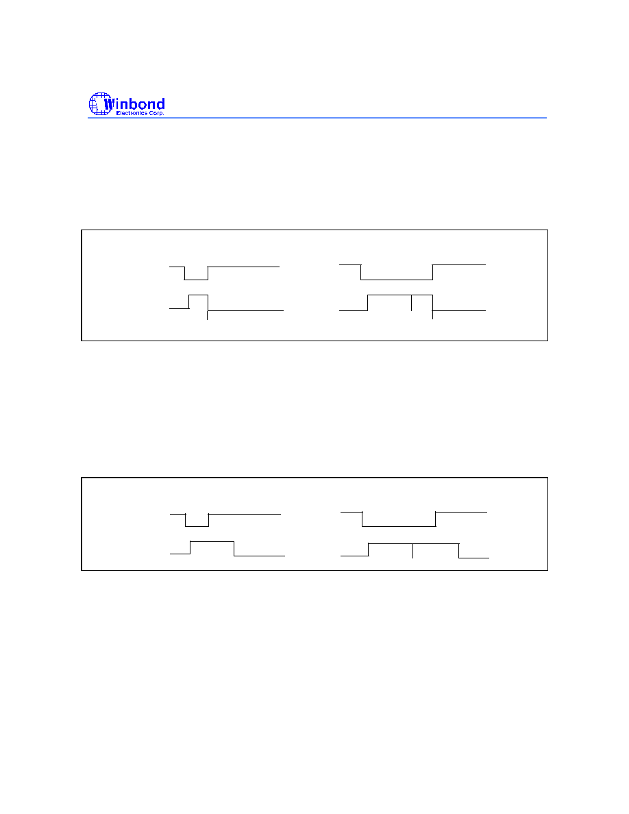
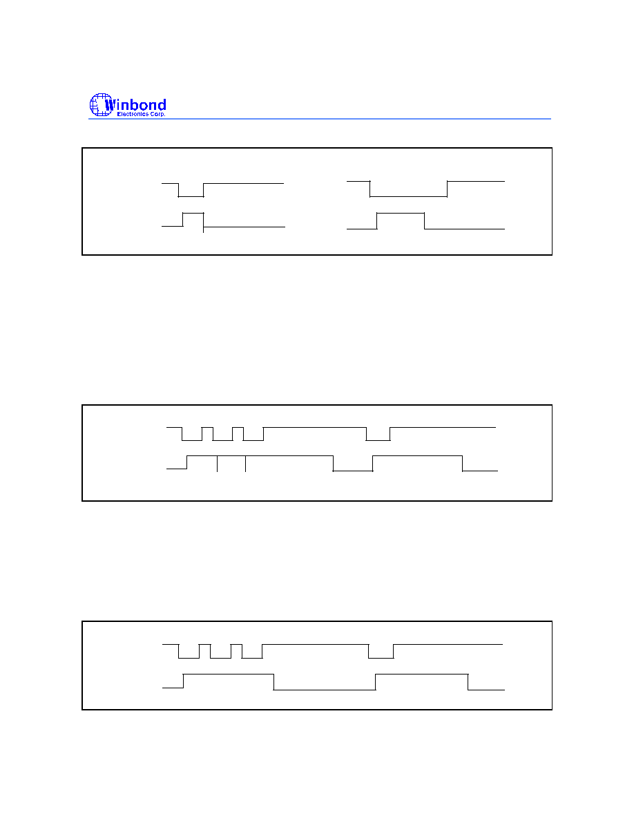
EXAMPLE1: Four playing mode settings:
a. One-Shot Trigger Mode
0: LD EN, 0x01 ; Enable TG1 falling edge input only.
H4 + sound1 + T4
END
The timing diagram for this example is shown below:
TG1:
TG1:
AUD:
AUD:
Sound 1
case 1:
case 2:
Sound 1
W528SXX
Publication Release Date: Nov 2000
- 11 - Revision A1
b. Level-Hold Trigger Mode
0: LD EN, 0x11 ; Enable TG1 rising/falling edge input.
H4 + sound1 + T4
JP 0 ; Repeat sound1 until TG1 key released.
4: END ; As soon as TG1 key is released, execute this group entry.
The timing diagram is shown below:
TG1:
AUD:
Stop Immediately
Sound 1
case 1:
case 2:
TG1:
AUD:
Stop Immediately
c. Complete-Cycle Level Hold
0: LD EN, 0x01 ; Enable TG1 falling edge only.
H4 + sound1 + T4
JP 0 @TG1_LOW ; If TG1 status is low level voltage (trigger is pressed), then j ump
to 0;
if not, execute next instruction (END).
END
The timing diagram is shown below:
AUD:
TG1:
Sound 1
case 1:
case 2:
TG1:
AUD:
Sound 1
Sound 1
d. Single-Cycle Level Hold
0: LD EN, 0x11 ; Enable both falling and rising edge input of TG1.
H4 + sound1 + T4
END
�
�
�
4: END ; As soon as TG1 is key released, execute this group entry.
W528SXX
- 12 -
The timing diagram is shown below:
TG1:
AUD:
Sound 1
case 1:
case 2:
TG1:
AUD:
Stop Immediately
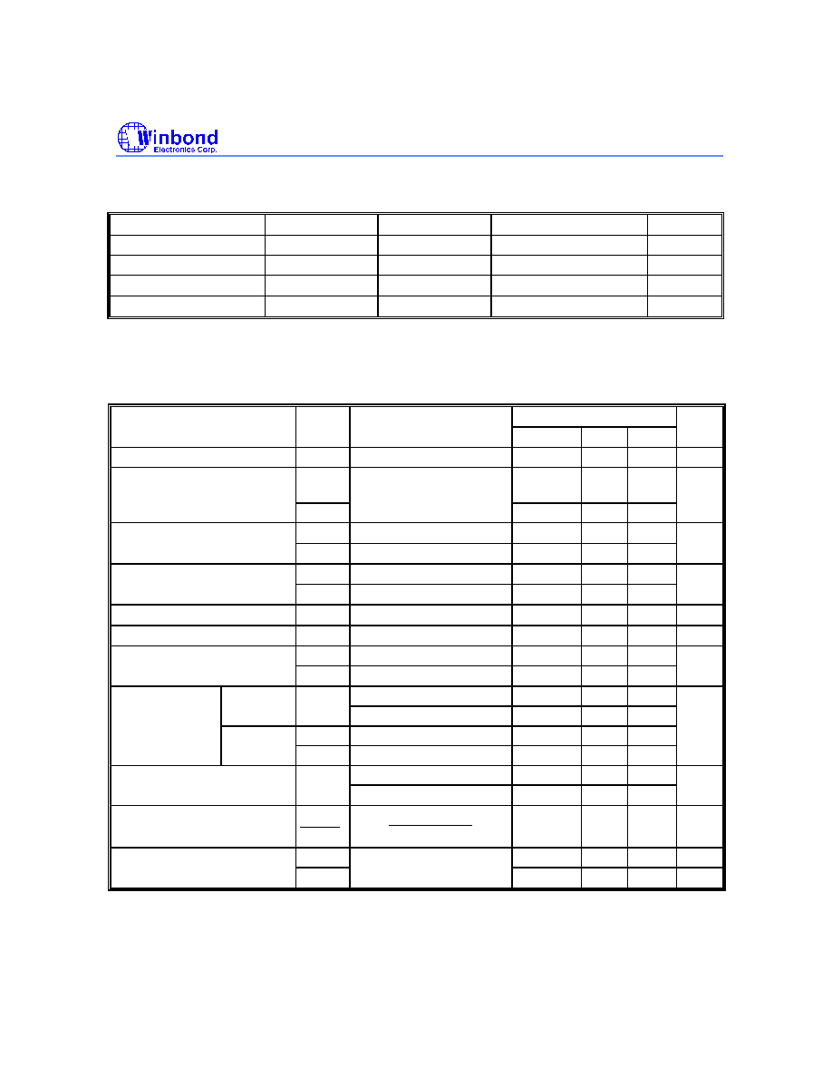
EXAMPLE 2: Retriggerable and Non-retriggerable setting
a. Retriggerable:
0: LD EN, 0x01 ; 0x01 = 00000001B, only TG1 falling edge interrupt is enabled.
END
�
�
�
END
The timing diagram is shown below:
TG1:
AUD:
Sound 1
Restart
Restart
Sound 1
b. Non-retriggerable:
0: LD EN, 0x00 ; 0x00 = 00000000B, TG1 falling edge interrupt is disabled.
�
�
LD EN, 0x11 ; Recover the TG1 falling and rising edge interrupt is enabled.
END
The timing diagram is shown below:
AUD:
TG1:
Sound 1
Sound 1
W528SXX
Publication Release Date: Nov 2000
- 13 - Revision A1
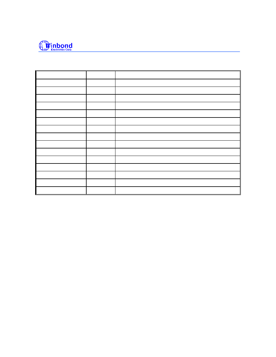
ABSOLUTE MAXIMUM RATINGS
PARAMETER
SYMBOL
CONDITIONS
RATED VALUE
UNIT
Power Supply
V
DD
-
V
SS
-
-0.3 to +7.0
V
Input Voltage
V
IN
All Inputs
V
SS
-0.3 to V
DD
+0.3
V
Storage Temp.
T
STG
-
-55 to +150
�
C
Operating Temp.
T
OPR
-
0 to +70
�
C
Note: Exposure to conditions beyond those listed under Absolute Maximum Ratings may adversely affect the life and reliability
of the device.
ELECTRICAL CHARACTERISTICS
(T
A
= 25
�
C, V
SS
= 0 V)
PARAMETER
SYM.
CONDITIONS
LIMITS
UNIT
MIN.
TYP. MAX.
Operating Voltage
V
DD
-
2.4
3
5.5
V
Input Voltage
V
IL
All Input Pins
V
SS
-0.3
-
0.3
V
DD
V
V
IH
0.7 V
DD
-
V
DD
Standby Current
I
DD1
V
DD
= 3V, No Playing
-
-
0.2
�
A
I
DD2
V
DD
= 5V, No Playing
-
-
0.4
Operating Current
I
OP1
V
DD
= 3V, No Load
-
-
400
�
A
I
OP2
V
DD
= 5V, No Load
-
-
800
Input Current for TG1
-
TG4
I
IN
V
DD
= 3V, V
IN
= 0V
-
-
6
�
A
SPK (D/A Full Scale)
I
O1
V
DD
= 4.5V, R
L
= 100
-4.0
-5.0
-6.0
mA
Output Current of STPC
I
OL
V
DD
= 3V, V
OUT
= 0.4V
1
-
-
mA
I
OH
V
DD
= 3V, V
OUT
= 2.7V
-0.5
-
-
LED1
I
O
V
DD
= 3V, V
OUT
= 1V
10
-
-
Output
LED2
V
DD
= 4.5V, V
OUT
= 1V
15
-
-
mA
Current
STPA
I
OL
V
DD
= 3V, V
OUT
= 0.4V
1
3
-
STPB
I
OH
V
DD
= 3V, V
OUT
= 2.7V
-1
-3
-
Oscillation Freq.
F
OSC
V
DD
= 3V, R
OSC
= Typ.
2.7
3
3.3
MHz
V
DD
= 4.5V, R
OSC
= Typ.
2.7
3
3.3
Oscillation Freq. Deviation
by Voltage Drop
F
F
OSC
OSC
F(3V) F(2.4)
F(3V)
-
0
4
7.5
%
Input Debounce Time
T
DEB1
F
OSC
= 3 MHz,
45
-
-
mS
T
DEB2
SR = 6 KHz
350
-
-
�
S
Notes:
1. Rosc = 430KOhm for all bodies in W528xxx
W528SXX
- 14 -
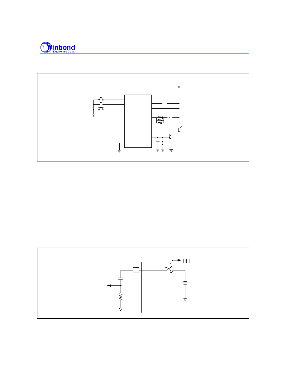
TYPICAL APPLICATION CIRCUIT
DD
Speaker
8 ohm
1/4 watt
OSC
Rosc
TG1
TG2
TG3
TG4/LED2/STPC
LED1
STPB
STPA
SPK
SS
Rs
C
s
8050 D
V
V
DD
39/100 ohm
R
V
Notes:
1. In principle, the playing speed determined by R
OSC
should correspond to the sampling rate during the coding phase.
The playing speed may be adjusted by varying R
OSC
, however.
2. Rs is an optional current-dividing resistor. If Rs is added, the resistance should be between 470 and 750
.
3. Cs is optional.
4. The DC current gain
of transistor 8050 ranges from 120 to 200.
5. All unused trigger pins can be left open because of their internal pull-high resistance.
6. R is used to limit the current on the LED. Case 1: V
DD
= 3V, R = 39
for 1/2/3 LEDs.
Case 2: V
DD
= 4.5V, R = 39
for 2/3 LEDs and R = 100
for 1 LED.
7. No warranty for production.
SUPPLEMENT
A. Power Bouncing
If an irregularity (such as bouncing) occurs in the power supply to V
DD
, as shown in the diagram, the
W528xxx may hang or the logic state machine may lock up. To return the chip to normal operation,
short V
DD
and V
SS
for the W528xxx and then release again.
Power bouncing
Battery
Power on
W528x
V
DD
Power on reset
W528SXX
Publication Release Date: Nov 2000
- 15 - Revision A1
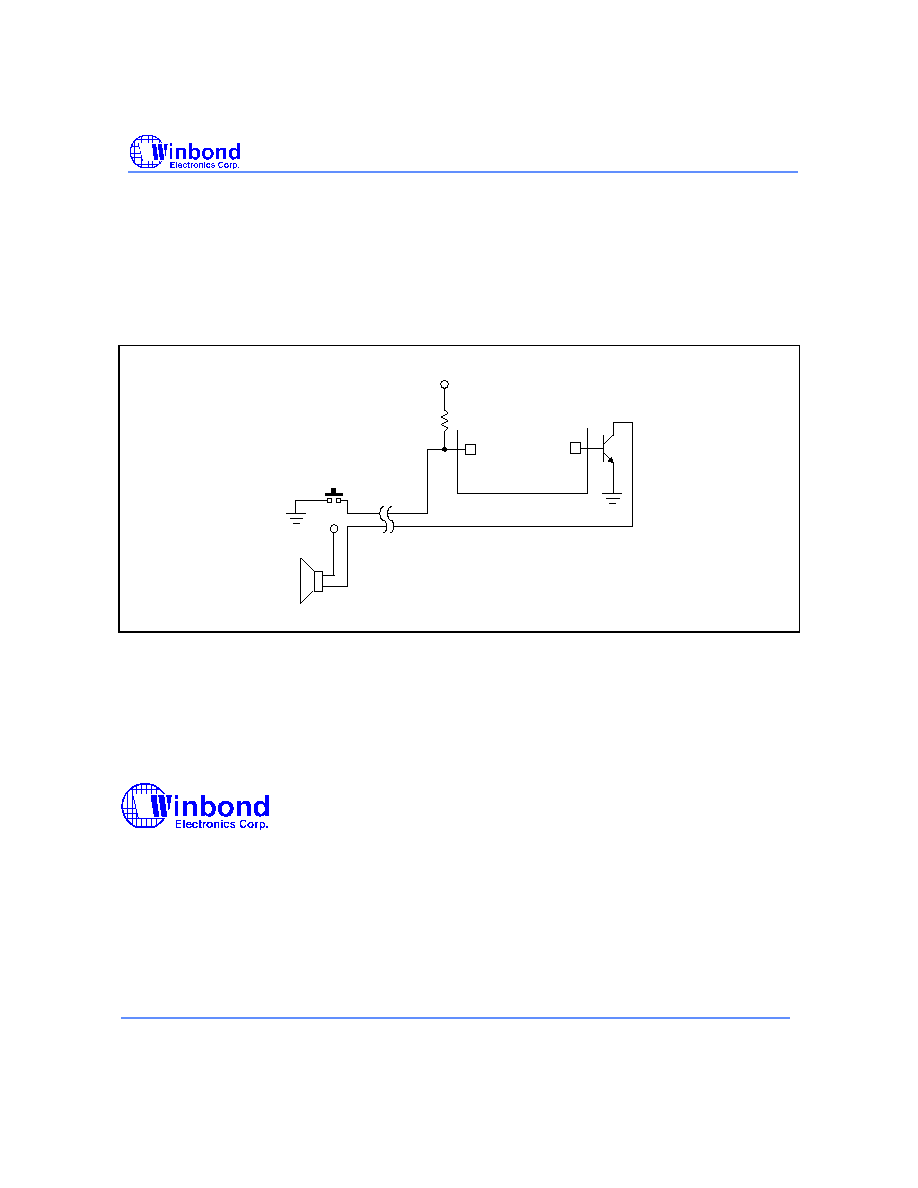
B. Ttigger Pin Coupling Effect
The trigger pins (TG1
-
TG4) are built-in 500K
pull high resistor.
If the wire of the input trigger is very close to the speaker wire in the application environment, the
coupling effect will occur. The input voltage of the trigger pin will be unstable, causing the trigger
operation to become abnormal.
An external pull high resistor (Ri) connecting the trigger pin and V
DD
can resolve this problem. The
value of the Ri depends on your application environment.
V
DD
SPK
TGn
V
DD
Ri
Headquarters
No. 4, Creation Rd. III,
Science-Based Industrial Park,
Hsinchu, Taiwan
TEL: 886-3-5770066
FAX: 886-3-5792697
http://www.winbond.com.tw/
Voice & Fax-on-demand: 886-2-27197006
Taipei Office
11F, No. 115, Sec. 3, Min-Sheng East Rd.,
Taipei, Taiwan
TEL: 886-2-27190505
FAX: 886-2-27197502
Winbond Electronics (H.K.) Ltd.
Rm. 803, World Trade Square, Tower II,
123 Hoi Bun Rd., Kwun Tong,
Kowloon, Hong Kong
TEL: 852-27513100
FAX: 852-27552064
Winbond Electronics North America Corp.
Winbond Memory Lab.
Winbond Microelectronics Corp.
Winbond Systems Lab.
2727 N. First Street, San Jose,
CA 95134, U.S.A.
TEL: 408-9436666
FAX: 408-5441798
Note: All data and specifications are subject to change without notice.