 | –≠–ª–µ–∫—Ç—Ä–æ–Ω–Ω—ã–π –∫–æ–º–ø–æ–Ω–µ–Ω—Ç: W528S10 | –°–∫–∞—á–∞—Ç—å:  PDF PDF  ZIP ZIP |

W528SXX Data Sheet
ADPCM VOICE SYNTHESIZER
(PowerSpeech
TM
)
Publication Release Date: June 13, 20033
- 1 - Revision A2
Table of Contents-
1.
GENERAL DESCRIPTION ......................................................................................................... 2
2.
FEATURES ................................................................................................................................. 2
3.
PAD CONFIGURATIONS ........................................................................................................... 3
4.
PAD DESCRIPTION ................................................................................................................... 4
5.
BLOCK DIAGRAM ...................................................................................................................... 5
6.
FUNCTIONAL DESCRIPTION ................................................................................................... 5
6.1
Instruction Set Description................................................................................................. 5
6.2
Conditional Instructions ..................................................................................................... 9
6.3
End Instruction................................................................................................................... 9
6.4
Program Structure Features and Execution Rules............................................................ 9
6.5
Mask Options................................................................................................................... 10
6.6
Speech Equation Description .......................................................................................... 10
6.7
Programmable Power-on Initialization............................................................................. 11
6.8
Progamming Examples ................................................................................................... 11
7.
ELECTRICAL CHARACTERISTICS......................................................................................... 14
7.1
Absolute Maximum Ratings............................................................................................. 14
7.2
DC Characteristics........................................................................................................... 14
8.
APPLICATION CIRCUIT........................................................................................................... 15
8.1
Supplement...................................................................................................................... 15
9.
REVISION HISTORY ................................................................................................................ 17
W528SXX
- 2 -
1. GENERAL DESCRIPTION
The W528Sxx family is programmable speech synthesis ICs that utilize the ADPCM coding method to
generate all types of voice effects.
The W528Sxx's LOAD and JUMP commands and four programmable registers provide powerful user-
programmable functions that make this chip suitable for an extremely wide range of speech IC
applications.
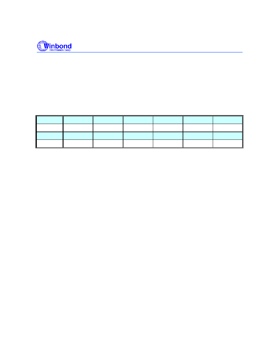
The W528Sxx family includes 9 kinds of part numbers with the same function except for the voice
duration shown below:
ITEM
W528S03
W528S05
W528S08A
W528S10
W528S12
W528S15
Second
3 Sec
5 Sec
8 Sec
10 Sec
12 Sec
15 Sec
ITEM
W528S20
W528S25
W528S30
Second
20 Sec
25 Sec
30 Sec
Note: The voice durations are estimated by various sampling rate.
2. FEATURES
∑ Programmable speech synthesizer
∑ Wide operating voltage range: 2.4 to 5.5 volts
∑ 4-bit ADPCM synthesis method
∑ Provides 4 direct trigger inputs that can easily be extended to 8 or 12 matrix trigger inputs
∑ Two trigger input debounce times (20 to 40 mS or 160 to 320 µS) can be set
∑ Provides up to 2 LEDs and 3 STOP outputs
∑ Every LED pin can drive 3 LEDs simultaneously
∑ LED flash frequency: 3 Hz
∑ AUD output current: 5 mA
∑ Flexible functions programmable through the following:
- LD (load), JP (jump) commands
- Four registers: R0, EN, STOP, and MODE
- Conditional instructions
- Speech equation
- END instruction
- Global repeat (GR) setting
- Output frequency and LED flash type setting
∑ Programmable power-on initialization (POI) (can be interrupted by trigger inputs)
∑ POI delay time of 160 mS ensures stable voltage when chip is powered on
∑ Can be programmed for the following functions:
W528SXX
Publication Release Date: June 13, 2003
- 3 - Revision A2
- Interrupt or non-interrupt for rising or falling edge of each trigger pin (this feature determines
retriggerable, non-retriggerable, overwrite, and non-overwrite features of each trigger pin)
- Four playing modes:
One Shot (OS)
Level Hold (LH)
Single-cycle level hold (S_LH)
Complete-cycle level hold (C_LH)
- Stop output signal setting
- Serial, direct, or random trigger mode setting
∑ Four frequency options (4/4.8/6/8 KHz) and LED On/Off control can be set independently in each
GO instruction of speech equation
∑ Independent control of LED1 and LED2
∑ Total of 256 voice group entries available for programming
∑ Provides the following mask options:
- LED flash type: synchronous/alternate
- LED1 section-controlled: Yes/No
- LED2: section-controlled/STPC-controlled
- LED volume-controlled: No/Yes
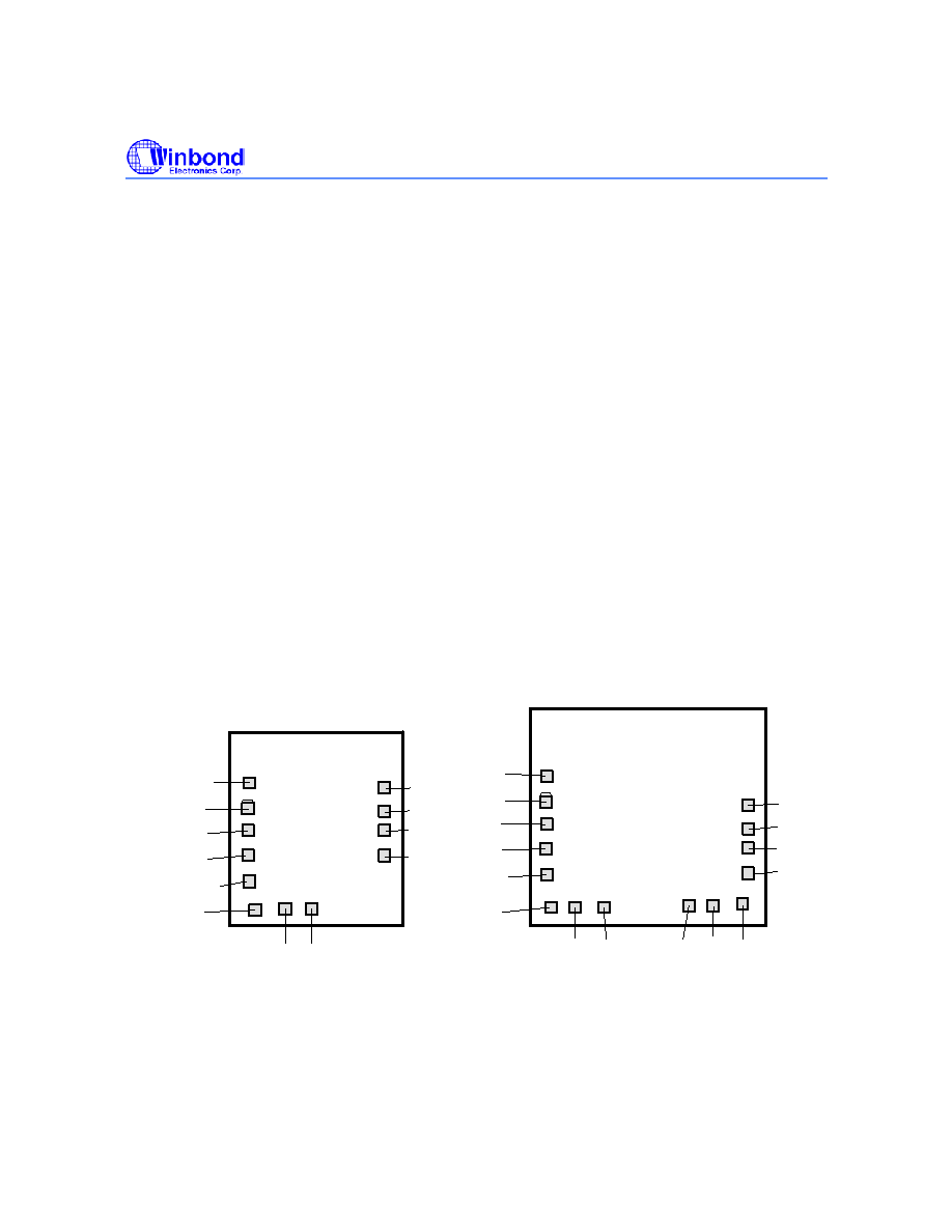
3. PAD CONFIGURATIONS
TG4/LED2/STPC
TEST
TG1
TG2
TG3
LED1
STPB
STPA
SPK
V
V
OSC
TEST4
TG1
TG2
TG3
TG4/LED2/STPC
LED1
STPB STPA
SPK
TEST1 TEST2
V
V
OSC
TEST3
DD
SS
DD
SS
W528S15 ~ S30
W528S03 ~ S12
Note: TEST3 is /RESET pin.
W528SXX
- 4 -
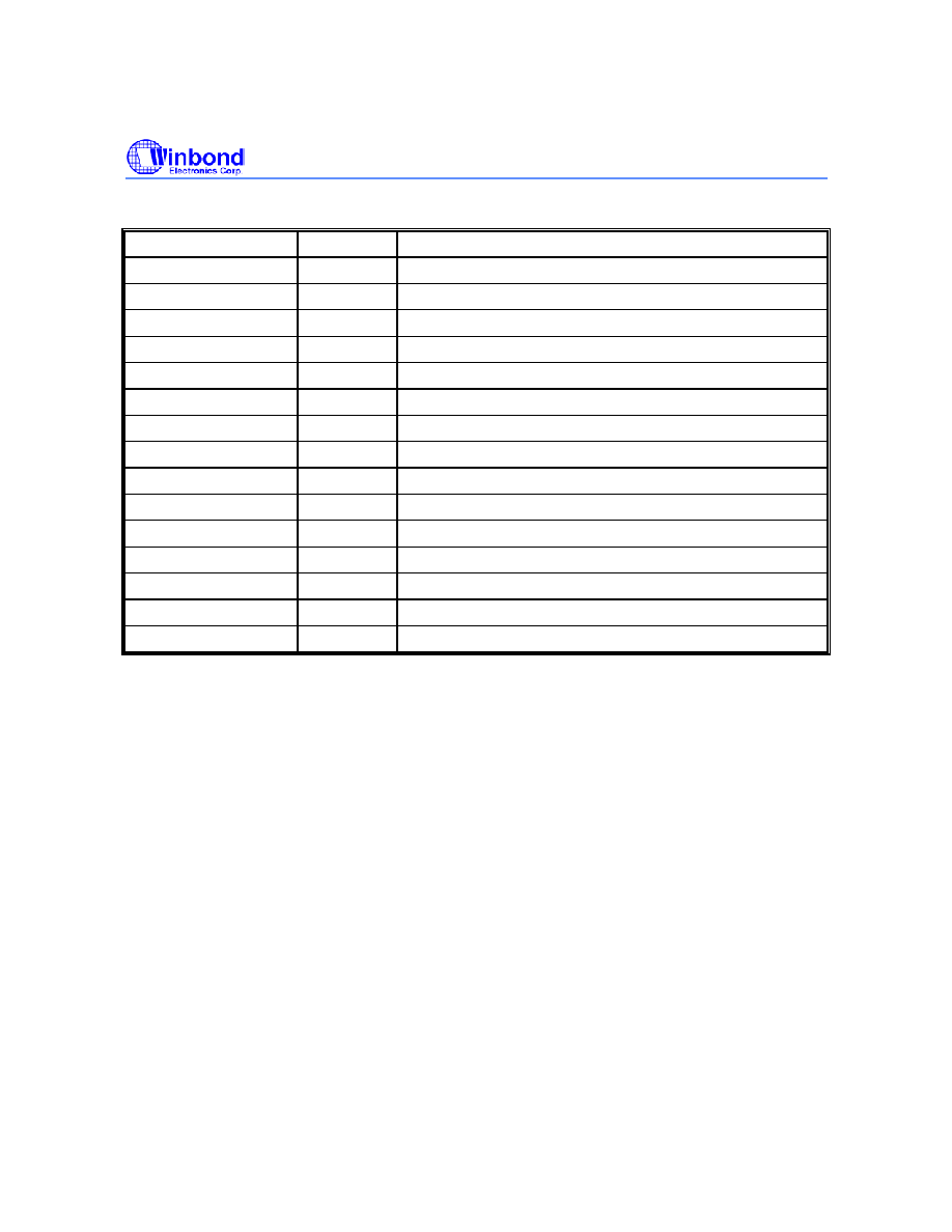
4. PAD DESCRIPTION
PAD NAME
I/O
FUNCTION
TG1
I
Trigger Input 1
TG2
I
Trigger Input 2
TG3
I
Trigger Input 3
TG4/LED2/STPC I/O Trigger
Input 4 or LED 2 or Stop Signal C
LED1 O
LED
1
STPB
O
Stop Signal B
STPA
O
Stop Signal A
SPK
O
Current Output for Speaker
V
SS
-
Negative Power Supply
V
DD
-
Positive Power Supply
OSC
I
Oscillation Frequency Control
*Test1 -
Test
Pin
*Test2 -
Test
Pin
*Test3
-
Test Pin or /Reset Pin
Test4 -
Test
Pin
* These pads only exist in W528S15 ~ W528S30.
W528SXX
Publication Release Date: June 13, 2003
- 5 - Revision A2
5. BLOCK DIAGRAM
OSC
TIMING
GENERATOR
DATA ROM
TG1
TG2
TG3
LED1
TG4/LED2/STPC
CONTROLLER
COUNTER
REGISTER
STPA
STPB
SYNTHESIZER
ADPCM
CONVERTER
REGISTER
SPK
& SHIFT
SHIFT
D/A
V
V
*TEST1
DD
SS
*TEST2
*TEST3
TEST4
* These pins only exist in W528S15 ~ W528S30.
6. FUNCTIONAL DESCRIPTION
The W528Sxx family provides up to four direct trigger pins, which can be extended to eight or twelve
matrix trigger inputs, up to three stop signal output pins, an LED section control, and powerful
programmable features. The JUMP and LOAD commands and four programmable registers can be
used to program the desired playing mode, stop output signal form, LED flash type, and trigger pin
interrupt modes.
The chip's programmable features can also be used to develop new, customized functions for a wide
variety of innovative applications.
6.1 Instruction Set Description
This section describes three types of instructions:
∑
Unconditional instructions, which are executed immediately after they are issued.
∑
Conditional instructions, which are executed only when the conditions specified in the instructions
are
satisfied.
∑
END instruction, which is used to stop all device activity.