
W536020K/030K/060K/090K/120K
VOICE/MELODY/LCD CONTROLLER
(ViewTalk
TM
Series)
Publication Release Date: May 21, 2003
- 1 -
Revision A3
Table of Contents-
1.
GENERAL DESCRIPTION ......................................................................................................... 2
2.
FEATURES ................................................................................................................................. 3
3.
BLOCK DIAGRAM ...................................................................................................................... 5
4.
PAD DESCRIPTION ................................................................................................................... 6
5.
ELECTRICAL CHARACTERISTICS........................................................................................... 9
5.1
Absolute Maximum Ratings............................................................................................... 9
5.2
DC Characteristics............................................................................................................. 9
5.3
AC Characteristics........................................................................................................... 11
6.
TYPICAL APPLICATION CIRCUITS ........................................................................................ 14
6.1
Sub Clock with RC Mode................................................................................................. 14
6.2
Sub Clock with Crystal Mode........................................................................................... 15
7.
REVISION HISTORY ................................................................................................................ 16

W536020K/030K/060K/090K/120K
- 2 -
1. GENERAL DESCRIPTION
The W536XXXK, a member of ViewTalk
TM
family, is a high-performance 4-bit micro-controller (uC)
with built-in speech unit, melody unit and 40seg * 8 com LCD driver unit which includes internal
regulator, pump circuit and dedicated one page LCD RAM. The 4-bit uC core contains dual clock
source, 4-bit ALU, two 8-bit timers, one 14 bits divider, maximum 24 pads for input or output, 8
interrupt sources and 8-level nesting for subroutine/interrupt applications. Speech unit, integrated as
a single chip with maximum 128 seconds (based on 6.4K sample rate with 5 bits MDPCM), is capable
of expanding to 512 seconds speech addressed by external memory W55XXX with serial bus
interface.
It can be implemented with Winbond Power Speech using MDPCM algorithm. Melody unit provides
dual tone output and can store up to 1k notes. Power reduction mode is also built in to minimize power
dissipation. It is ideal for games, educational toys, remote controllers, watches, clocks and other
application products which incorporate both LCD display and speech.
Body W536020K
W536030K
W536060K
W536090K
W536120K
Voice
20 sec
30 sec
60 sec
90 sec
120 sec
I/O pad
4I/O,8I
(RA/RC/RD)
4I/O, 8I
(RA/RC/RD)
8io, 8i
(RA/RB/RC/RD)
8I/O, 8I, 8O
(RA/RB/RC/RD/RE/
RF)
8I/O, 8I, 8O
(RA/RB/RC/RD/
RE/RF)
WDT disable/Enable
(Mask Option)
Y Y Y
Y Y
Sub-clock
RC/XTAL mode
(Mask Option)
Y Y Y
Y
Y
RD port shared as
serial bus
(Mask Option)
Y(1) Y(1)
N
N N
(2)
Tri-state serial bus
(Mask Option) (3)
Y Y N
Y Y
Cascaded Voice ROM
through serial bus (2)
N Y(1) N
N
Y
Notes:
1. Share 3 pads of RD port (RD1/CLK, RD2/DATA and RD3/ADDR)
2. Dedicate serial bus 3 pads (CLK, DATA and ADDR) to interface with W55XXX. Cascaded Voice ROM can help to expand
voice up to 512 sec by W55XXX chip.
3. Tri-state serial bus mask option can float serial bus while voice playing is no active. Let this mask option is disabled to get
minimum power consumption in general.

W536020K/030K/060K/090K/120K
Publication Release Date: May 21, 2003
- 3 -
Revision A3
2. FEATURES
� Operating voltage: 2.4 volt ~ 5.5 volt
� Watch dog disabled/enabled by mask option
� Dual clock operating system
- Main clock with Ring/Crystal (400 KHz to 4 MHz)
- Sub-clock with 32.768 KHz RC/Crystal by mask option
� Memory
- Program ROM (P-ROM): 16K � 20 (ROM Bank0)
- Data RAM (W-RAM): 1K � 4 bit
(RAM Bank 0 is 512 nibbles from 0: 000~0: 1FF and 0: 380~0:3FF are mapped to specia
register.
RAM Bank F is 512 nibbles from F: 200~F: 3FF either data RAM or dedicated to script
kernel)
- LCD RAM (L-RAM): 80� 4 bit (RAM Bank1 from 200~24F)
� Maximum 24 input/output pads
- Ports for input only: 8 pads (RC, RD port; RD1~3 can share as serial bus for external
memory W55XXX interface @W5360020/30K)
- Ports for output only: 8 pads (RE & RF port; W536090K/120K available only)
- Ports for Input/output: 8 pads (RA and RB port; RB port is available for W536060/090K/
120K only)
� Power-down mode
- Hold mode (except for 32KHz oscillator)
- Stop mode (including 32KHz oscillator and release by RD or RC port)
� Eight types of interrupts
- Five internal interrupts (Divider, Timer 0, Timer 1, Speech, Melody)
- Three external interrupts (Port RC, RD, RA)
� One built-in 14-bit clock frequency divider circuit
� Two built-in 8-bit programmable countdown timers
- Timer 0: one of two clock sources (FOSC/4 or FOSC/1024) can be selected
- Timer 1: built-in auto-reload function includes internal timer, external event counter from
RC.0
� Built-in 18/14-bit watchdog timer for system reset.
� Powerful instruction sets
� 8-level subroutine (including interrupt) nesting
� LCD driver unit capability
- VLCD higher than (V
DD
-0.5V)
- Built-in voltage regulator to V2 pad
- 40 seg � 8 com

W536020K/030K/060K/090K/120K
- 4 -
- 1/8 or 1/4 duty, 1/4 or 1/3 bias, internal pump circuit option by special register
- COM 4~ 7 and SEG16~39 can be shared as general input/output by special register
- Either uC ROM or voice ROM used as LCD picture
� Speech function
- Provided 640K / 1M/ 2M/ 3M/ 4M bits Voice ROM for W536020K/030K/060K/090K/120K
based on 5 bits MDPCM algorithm
- Voice ROM (V-ROM) available for uC data or LCD picture data.
- Maximum 8*256 Label/Interrupt vector (voice section number) available
- Provide two types of speech busy flag to either each GO or each trigger
- Maximum up to 16M bits speech address capability interface with external memory
W55XXX through serial bus.
� Melody function
- Provide 1K notes (22bits/note) dedicated melody ROM
- Provide two types of melody busy flag to uC either each note or each song
- Provide 6 kinds of beat, 16 kinds of tempo, and pitch range from G3# to C7
- Tremolo, triple frequency and 3 kinds of percussion available
- Maximum 31 songs available
� Can mix speech with melody
� Multi-engine controller
� Direct driving speaker/buzzer or DAC output
� Chip On Board available

W536020K/030K/060K/090K/120K
Publication Release Date: May 21, 2003
- 5 -
Revision A3
3. BLOCK DIAGRAM
XIN
XOUT X32I X32O
LCD DRIVER
PC
STACK
(8 Levels)
Timer 0
Timing
Generator
SEG0~39
V3,V5,V6
Timer 1
Watch Dog
ALU
ACC
Divide
ROM
16K*20Bit
DH1,DH2
COM0~7
LCDRAM
80*4 bit
Data RAM
1K*4 bit
Special Register
HCF
HEF
IEF
EVF
FLAG1
PSR0
MR0
PEF
FLAG0
LPX3
PM0
LPX2
LPX0 LPX1
PORT RA
VLCD PUMP &
REGULATOR
TONE
TEST
RA0~3
VDD
RES
VDDP
VSS
LPX4
V2
PORT RC
PORT RD
RC0~3
RD0~3
LPX5
LPY0
LPY1
SPC
MLD
Dual
Tone
Melody
MLD_play
MLD_busy
MDPCM
Speech
SPC_pla
y
SPC_bus
y
PWM1/DAC
PWM2
ROSC
Parallel
to Serial
VSSP
VHI
Interrupt ,Hold &
Stop Control
RE0~3
RF0~3
PORT RB
RB0~3
PORT RE
PORT RF
ADDR
CLK
DATA
PWM/
DAC
MIX
Block
Voice ROM
(640K/1M/3M/
4M)
W536020K/030K/060K/090K/120K
- 6 -
4. PAD DESCRIPTION
SYMBOL I/O
FUNCTION
XIN/RXIN I
Input pad for main clock oscillator. It can be connected to crystal when
crystal mode is selected (SCR0.2 = 1), otherwise connect a resistor to
V
DD
to generate main system clock while Ring mode is selected (SCR0.2
= 0 and default). Oscillator can be enabled or stopped by set SCR0.1 to
1 or clear to 0 separately. External capacitor connects to start oscillation
and get more accurate clock when crystal mode
XOUT O
Output pad for oscillator which is connected to another crystal pad when
in crystal mode. External capacitor connects to start oscillation when in
crystal mode.
X32I/RSUB1 I
32.768 KHz crystal input pad or external resistor node 1 by mask
option. External 15~20pF capacitor connects to start oscillation and get
more accurate clock when in crystal mode.
X32O/RSUB2 O
32.768 KHz crystal output pad or external resistor node 2 by mask
option. External 15~20pF capacitor connects to start oscillation when in
crystal mode.
RA0 ~ RA3/TONE
(9)
I/O
General Input/Output port specified by PM1 register. If output mode is
selected, PM0 register bit 0 can be used to specify CMOS/NMOS driving
capability option. Initial state is input mode. RA3 may be uses as TONE
if bit 0 of MR0 special register is set to logic 1. An interrupt source.
RB0 ~ RB3
(9)
I/O
General Input/Output port specified by PM2 register. If output mode is
selected, PM0 register bit 1 can be used to specify CMOS/NMOS driving
capability option. Initial state is input mode (W536060K/090K/120K only.)
RC0 ~ RC3
I
4-bit schmitter input with internal pull high option specified by PM3
register bit 2. Each pad has an independent interrupt capability specified
by PEFL special register. Interrupt and STOP mode wake up source.
RC0 is also the external event counter source of Timer1.
RD0
RD1/CLK
RD2/DATA
RD3/ADDR
(4)
I
4-bit schmitter input port with internal pull high option specified by PM3
register bit 3. Each pad has an independent interrupt capability specified
by PEFH special register. Interrupt and STOP mode wake up source.
RD1~3 will be shared as the external memory W55XXX interface pads
while RD port shared as serial bus mask option is enabled
@W536020K/030K.
For W536020K/030K only, "Tri-state serial bus" mask option can use to
float ADDR/CLK/DATD while "RD port shared as serial bus" mask option
is enabled.
RE0~RE3
(9)
O
Output port only. PM3 register bit 0 can be used to specify CMOS/NMOS
driving capability option. (W536090K/120K only)
RF0~RF3
(9)
O
Output port only. PM3 register bit 1 can be used to specify CMOS/NMOS
driving capability option. (W536090K/120K only)

W536020K/030K/060K/090K/120K
Publication Release Date: May 21, 2003
- 7 -
Revision A3
PAD Description, continued
SYMBOL I/O
FUNCTION
RES
I
System reset pad, active low with internal pull-high resistor.
TEST
I
Test pad. Active high with internal pull low resistor.
ROSC I
Connect resistor to V
DD
pad to generate speech or melody playing
clock source.
PWM1/DAC O
While speech or melody is active, PWM1/DAC is speaker direct driving
output or DAC output controlled by voice output file.
PWM2 O
While speech or melody is active, PWM2 is another speaker direct
driving output.
ADDR (5)
O
External serial memory address write clock for voice extension
(W536120K only).
CLK (5)
O
External serial memory address read clock for voice extension.
(W536120K only).
DATA (5)
I/O
External serial memory data in/out for voice extension (W536120K
only).
SEG0
-SEG15
O
Dedicated LCD segment output pads.
SEG16/PORTN.0
SEG19/PORTN.3
O/O
LCD segment output pads, and can be shared as general output by
register LCDM3 bit 1. Default function is segment pad.
SEG20/PORTM.0
SEG23/PORTM.3
O/I
LCD segment output pads, and can be shared as general input by
register LCDM3 bit 0. Default function is segment pad and PM5.1=0 to
inhibit LCD waveform abnormal.
SEG24/PORTL.0
SEG27/PORTL.3
O/O
LCD segment output pads, and can be shared as general output by
register LCDM2 bit 3. Default function is segment pad.
SEG28/PORTK.0
SEG31/PORTK.3
O/I
LCD segment output pads, and can be shared as general input by
register LCDM2 bit 2. Default function is segment pad and PM5.0=0 to
inhibit LCD waveform abnormal.
SEG32/PORTJ.0
SEG35/PORTJ.3
O/IO
LCD segment output pads, and can be shared as general input/output
by register LCDM2 bit 1. PM4 register is used to select input or output
while shared I/O function is active. Default function is segment pad and
PM4.3 = 0 to inhibit LCD waveform abnormal.
SEG36/PORTI.0
SEG39/PORTI.3
O/IO
LCD segment output pads, and can be shared as general input/output
by register LCDM2 bit 0. PM4 register is used to select input or output
while shared I/O function is active. Default function is segment pad and
PM4.2 = 0 to inhibit LCD waveform abnormal.
W536020K/030K/060K/090K/120K
- 8 -
PAD Description, continued
SYMBOL I/O
FUNCTION
COM0
-COM3
O
LCD common signal output pads either 1/8 duty or 1/4duty. The LCD
frame rate is controlled by LCDM1 register, and default value LCDM1 =
0111b with 64Hz frame rate.
COM4/PORTO.0
COM7/PORTO.3
O/I
LCD common signal output pads, or shared as general input by register
LCDM3.2 when in 1/4 duty mode. Default function is common function
and PM5.2 = 0 to inhibit LCD waveform abnormal.
DH1, DH2 (6)
O
Connection terminal for voltage double capacitor with 0.1uF. The DH2
connects to capacitor positive node and DH1 negative node if polar
capacitor is used.
VHI I
Connect to V6 (LCD's VLCD) or V
DD
which has higher voltage, to make
sure there is no any abnormal leakage current appearance.
V3 O
LCD COM/SEG output driving voltage. Need an external 0.1uF
capacitor when 1/4 bias. (LCDM0.1 = 1)
V5 V6 (6)
O
LCD COM/SEG output driving voltage. Need an external 0.1uF
capacitor to every pad terminal.
V2 (6)
I/O
Voltage regulator output pad. An external capacitor is a must. Output
level can be controlled from 0~Fh by LCDM4 register. If internal pump is
enabled (LCDM3.3 = 0 and default value), LCD operating voltage
(VLCD) will be 3*V2 or 4*V2 depending on 1/3 bias or 1/4 bias. A
limitation should be noted that VLCD must be higher than (V
DD
-0.5v) to
avoid chip leakage current. While external reference voltage is selected
(LCDM3.3 = 1), V2 pad input voltage can not be over 1.5 Volt to inhibit
chip damage.
V
SSP
(7)
I
Power ground for PWM or DAC playing output.
V
SS
(7)
I
Power ground
V
DDP
(7)
I
Power source for PWM or DAC playing output.
V
DD
(7)
I
Power Source
Notes:
(4)
RD1~3 are shared as CLK/DATA/ADDR to interface with W55XXX @W536020K/030K.
(5) @W536120K
only
(6)
0.1uF is default value, and capacitor value should be larger than 0.1uF if LCD dot size over 0.5mm * 0.5mm.
(7)
External application circuit should connect together, please refer to APPLICATION CIRCUIT. To sure chip operation
properly, please bond all V
DD
, V
DDP
, V
SS
and V
SSP
pads and connect V
SS
and V
SSP
from chip outside PCB circuit.
(8)
VHI pad is bonded to V6 or V
DD
.
(9)
When working at NMOS open drain mode, external pull high voltage can't bigger than V
DD
to avoid leakage current.

W536020K/030K/060K/090K/120K
Publication Release Date: May 21, 2003
- 9 -
Revision A3
5. ELECTRICAL CHARACTERISTICS
5.1 Absolute Maximum Ratings
PARAMETER RATING
UNIT
Supply Voltage to Ground Potential
-0.3 to +7.0
V
Applied Input/Output Voltage
-0.3 to +7.0
V
Power Dissipation
120
mW
Ambient Operating Temperature
0 to +70
�C
Storage Temperature
-55 to +150
�C
Note: Exposure to conditions beyond those listed under Absolute Maximum Ratings may adversely affect the life and reliability
of the device.
5.2 DC Characteristics
(V
DD
-V
SS
= 3.0V, no load, FM = 4 MHz with Ring mode, Fs = 32.768 KHz, with Xtal mode, T
A
= 25
� C, STN LCD panel on with
dot size 0.5mm*0.5mm; unless otherwise specified)
PARAMETER SYM.
CONDITIONS
MIN. TYP. MAX. UNIT
Op. Voltage
V
DD
2.4
5.5
V
Op. Current
I
OP1
Dual clock with crystal
-
600
700
�A
(No Load, no Voice, no)
Dual clock with Ring
type
600
700
Melody)
Sub-clock only, LCD off
40
50
Sub-clock only, LCD on
70
90
Hold Mode Current
(No Load, LCD OFF)
I
OP2
Sub-clock active only
3
5
�A
Hold Mode Current
(No load, LCD ON)
I
OP3
Sub-clock active only
35
uA
Stop Mode Current
I
OP4
LCD auto off
1
�A
CLK/ADDR Output High
Current
Io
H1
Vout = 2.7V
-0.8
mA
CLK/ADDR Output low
Current
Io
L1
Vout = 0.4V
0.8
mA
Input Low Voltage
V
IL
-
V
SS
- 0.3 V
DD
Input High Voltage
V
IH
- 0.7
-
1
V
DD
Port RA, RB, RE, RF Output
Low Voltage
V
ABL
I
OL
= 2.0 mA
-
-
0.4
V
Port RA, RB, RE, RF Output
High Voltage
V
ABH
I
OH
= -2.0 mA
2.4
-
-
V

W536020K/030K/060K/090K/120K
- 10 -
DC Characteristics, continued
PARAMETER SYM.
CONDITIONS
MIN. TYP. MAX. UNIT
Pull-up Resistor
R
CD
Port RC, RD
200
300
400
K
Share Output RI, RJ, RL,
RN, RP Sink Current
I
OL3
V
OL
= 0.4V
-300
uA
RES Pull-up Resistor
R
RES
- 50
100
200
K
PWM1/2 Source Current (8)
I
SPH
Volume Option = 00
-20
mA
(R
LOAD
=8
between PWM1
Volume Option = 01
-70
And PWM2)
Volume Option = 10
-110
Volume Option = 11
-135
PWM1/2 Sink Current (8)
I
SPL
Volume Option = 00
20
mA
(R
LOAD
= 8
between PWM1
Volume Option = 01
70
And PWM2)
Volume Option = 10
110
Volume Option = 11
135
DAC output Current
I
DAC
V
DD
= 3V, RL = 100ohm
-4
-5
-6
mA
LCD Supply Current
I
LCD
No Load, All Seg. ON
-
50
-
�A
COM/SEG On Resistor
R
ON
I
OH
=
�50 �A
5K
10K
V2 Pad Output Voltage
V
RR
Depended on LCDM4
0.7
1.45
V
V2 Pad Output Deviation (9)
V
D1
No Load
� 5
%
V2 Pad Voltage Step
V
R2
LCDM4 increased 1
50
mV
V6 Pad Output Voltage
(LCD's VLCD depended on
V
LCD
1/3 Bias & no load
2.85
* V2
2.9
* V2
2.95
* V2
V
LCDM4 register) (9)
1/4 Bias & no load
3.8
* V2
3.85
* V2
3.9
* V2
V2 input voltage
V
EXT
LCDM3.3 = 1
1.5
V
Notes:
(8)
PWM current deviation will be
�20%.
(9)
Deviation is governed by LCD dot size. More larger LCD dot will get larger deviation..

W536020K/030K/060K/090K/120K
Publication Release Date: May 21, 2003
- 11 -
Revision A3
5.3 AC Characteristics
(V
DD
-V
SS
= 3.0V, no load, FM = 4 MHz with Ring mode, Fs = 32.768 KHz, with Xtal mode, T
A
= 25
� C, STN LCD on with dot size
0.5mm*0.5mm; unless otherwise specified)
PARAMETER SYM. CONDITIONS
MIN.
TYP.
MAX. UNIT
Sub-clock Frequency
F
SUB
Crystal type and X32IN
and X32O with 17pF
external cap.
32768 Hz
Main-clock Frequency
F
M
Ring type/Crystal type
400K
-
4M
Hz
Chip Operation Frequency
F
OSC
SCR0.0 = 1, F
SYS
= F
SUB
32768 Hz
SCR0.0 = 0; F
SYS
= F
MAIN
400K
-
4M
Instruction Cycle Time
T
CYC
One machine cycle
-
4/F
OSC
- S
Reset Active Width
T
RAW
FOSC = 32.768 KHz
1
-
-
�S
Interrupt Active Width
T
IAW
FOSC = 32.768 KHz
1
-
-
�S
Main clock Ring frequency
F
RXIN
RXIN = 680K
1M Hz
(10)
RXIN = 330K
2M
RXIN = 200K
3M
RXIN = 130K
4M
Sub-Clock RC Oscillator
F
RSUB
R
SUB
= 680K
32
KHz
Sub-Clock Oscillation Stable
Time @ Cold Start
F
STOP
R
SUB
= 680K
0.8 1 S
Frequency Deviation of
main-clock F
RXIN
2MHz
f
f
f(3V) f(2.4V)
f(3V)
-
10
%
Frequency Deviation of
main-clock F
RXIN
= 3 MHz
f
f
f(3V) f(2.4V)
f(3V)
-
15
%
Frequency Deviation of
main-clock F
RXIN
= 4 MHz
f
f
f(3V) f(2.4V)
f(3V)
-
20
%
ROSC Frequency
F
ROSC
R
OSC
=680K
3
MHz
Frequency Deviation of
F
ROSC
= 3MHz
f
f
f(3V) f(2.4V)
f(3V)
-
7.5
%
Frame frequency
F
LCD
LCDM1 = 0111 b(default)
64
Hz
Notes:
(10) The deviation will be +20% while V
DD
drops from 5.5V to 2.4V based on same resistor
W536020K/030K/060K/090K/120K
- 12 -
Iop Vs. Main clock RC mode
0
200
400
600
800
1000
1
2
3
4
Freq (MhZ)
Iop (uA)
3V
4.5V
Oscillation Freq Vs. Sub-Clock
20
24
28
32
36
40
44
560
620
680
750
820
1K
Rsub (Kohm)
Fsub (KhZ)
3V
4.5V
W536020K/030K/060K/090K/120K
Publication Release Date: May 21, 2003
- 13 -
Revision A3
Main Freq Vs. Rxin
0
1
2
3
4
5
6
130 150 160 200 330 680 2K 3K
RXIN (Kohm)
Fmain
(MhZ)
2.4V
3v
4.5V
5.5V
Voice Operating Freq. Vs. ROSC
2
2.5
3
3.5
4
4.5
470
560
680
910
ROSC (Kohm)
Freq (MhZ)
3V
4.5V
W536020K/030K/060K/090K/120K
- 14 -
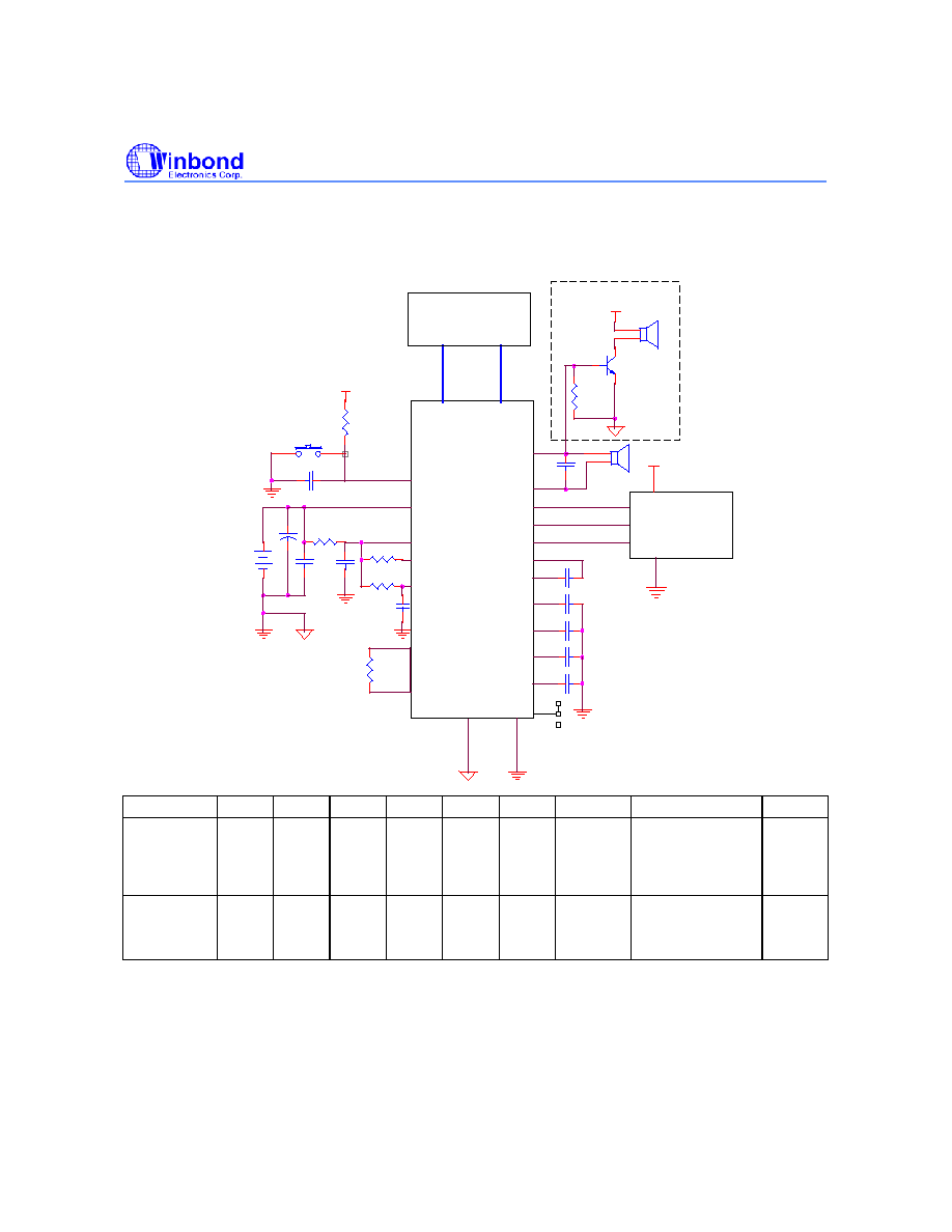
6. TYPICAL APPLICATION CIRCUITS
6.1 Sub Clock with RC Mode
1/4 bias, V
LCD
= 4.5V, V
DD
= 2.4~3.6V
VDDP
VDDP
VDDP
VDD
XIN
X32IO
X32IN
___
RES
PWM1/DAC
CLK/RD1
DATA/RD2
ADDR/RD3
W536XXXK
Rosc
CO
M
0
~
7
SE
G
0
~
3
9
PWM2
DH1
DH2
V6
V5
V2
V3
VSS
P
VS
S
SPEAKER
SPEAKER
R2
R1
R4
C3
R5
Q1
8050
SWITCH
470
C4
R3
C5
C6
Battery
1
2
C2
C1
C13
C12
C10
C11
C9
VHI
V6
VDD
(*3)
(*2)
(*1)
(*4)
40SEG*8COM
LCD Panel
(*4)
(*5)
W55MXX
VDDP
COMPONENT C1 C2~C4 C5~C6 C7~C8 C9~C13
R1
R2
R3
R4
Value
V
DD
= 3V
4.7uF 0.1uF
100pF
- 0.1~1uF
680K 655K
680K
/1MHz
350K
/2MHz
215K
/3MHz
150K/4MHz
100
Value
V
DD
= 4.5V
4.7uF
0.1uF
100pF
- 0.1~1uF
680K 675K
750K/1MHz
350K/2MHz
225K/3MHz
160K/4MHz
100
Notes:
1. C9~C13 depends on LCD panel dot size.
2. Option R5 equals to 100
if high noise immunity is needed.
3. For DAC option application.
4. To ensure that three batteries function well in W536F20 demo board. C
6
should stay close to pad PWM/PWM2 at its best.
Under the mask ROM version, C
5
and C
6
can be skipped.
5. Sure chip operation properly, please bond all V
DDP
, V
DD
, V
SSP
and V
SS
; and connect V
SSP
pad to V
SS
from external PCB circuit.
W536020K/030K/060K/090K/120K
Publication Release Date: May 21, 2003
- 15 -
Revision A3
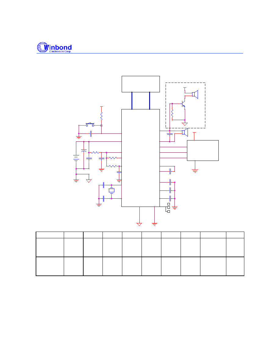
6.2 Sub Clock with Crystal Mode
1/3 bias, V
LCD
= 3V, V
DD
= 3.6~5.4V
VDDP
VDDP
VDDP
VDD
XIN
X32IO
X32IN
___
RES
PWM1/DAC
CLK/RD1
DATA/RD2
ADDR/RD3
VSS
VSSP
W536XXXK
Rosc
CO
M
0
~
3
S
E
G
0~39
PWM2
V2
V3
V5
DH2
DH1
SPEAKER
SPEAKER
R1
R4
C3
R5
Q1
8050
SWITCH
470
C4
R3
C5
C6
Battery
1
2
C2
C1
C12
C11
C10
C9
32K
C7
C8
VDD
V6
VHI
(*3)
(*2)
(*1)
(*4)
40SEG*4COM
LCD Panel
(*4)
(*5)
W55MXX
VDDP
Component
C1 C2~C4 C5~C6 C7~C8 C9~C12 R1
R2
R3
R4
Value
V
DD
= 3V
4.7uF 0.1uF
100pF
15~30PF 0.1~1uF 680K -
680K/1MHz
350K/2MHz
215K/3MHz
150K/4MHz
100
Value
V
DD
= 4.5V
4.7uF 0.1uF
100pF
15~30PF 0.1~1uF 680K -
750K/1MHz
350K/2MHz
225K/3MHz
160K/4MHz
100
Notes:
1. C9~C12 depends on LCD panel dot size.
2. Option R5 equals to 100
if high noise immunity is needed.
3. For DAC option application.
4. To ensure that three batteries function well in W536F20 demo board. C
6
should stay close to 5. pad PWM/PWM2 at its best.
Under the mask ROM version, C
5
and C
6
can be skipped.
5. Sure chip operation properly, please bond all V
DDP
, V
DD
, V
SSP
and V
SS
; and connect V
SSP
pad to V
SS
from external PCB circuit.
W536020K/030K/060K/090K/120K
- 16 -
7. REVISION HISTORY
VERSION DATE
WRITER
DESCRIPTION
A1
SEP. 18, 2000
Jimmy Chen
A2
NOV. 24, 2000
Jimmy Chen
Application circuit modify
A3
May 21, 2003
Jimmy Chen
Application circuit modify
Headquarters
No. 4, Creation Rd. III,
Science-Based Industrial Park,
Hsinchu, Taiwan
TEL: 886-3-5770066
FAX: 886-3-5665577
http://www.winbond.com.tw/
Taipei Office
TEL: 886-2-8177-7168
FAX: 886-2-8751-3579
Winbond Electronics Corporation America
2727 North First Street, San Jose,
CA 95134, U.S.A.
TEL: 1-408-9436666
FAX: 1-408-5441798
Winbond Electronics (H.K.) Ltd.
No. 378 Kwun Tong Rd.,
Kowloon, Hong Kong
FAX: 852-27552064
Unit 9-15, 22F, Millennium City,
TEL: 852-27513100
Please note that all data and specifications are subject to change without notice.
All the trade marks of products and companies mentioned in this data sheet belong to their respective owners.
Winbond Electronics (Shanghai) Ltd.
200336 China
FAX: 86-21-62365998
27F, 2299 Yan An W. Rd. Shanghai,
TEL: 86-21-62365999
Winbond Electronics Corporation Japan
Shinyokohama Kohoku-ku,
Yokohama, 222-0033
FAX: 81-45-4781800
7F Daini-ueno BLDG, 3-7-18
TEL: 81-45-4781881
9F, No.480, Rueiguang Rd.,
Neihu District, Taipei, 114,
Taiwan, R.O.C.
Information contained in this publication regarding device applications and the like is intended for suggestion
only and may be superseded updates. No representation or warranty is given and no liability is assumed by
Winbond Electronics Corp. with respect to the accuracy or use of such information, or infringement of patents
or other intellectual property.