 | –≠–ª–µ–∫—Ç—Ä–æ–Ω–Ω—ã–π –∫–æ–º–ø–æ–Ω–µ–Ω—Ç: W541E200 | –°–∫–∞—á–∞—Ç—å:  PDF PDF  ZIP ZIP |

PRELIMINARY W541E20X
4-BIT FLASH EPROM MICROCONTROLLER
Publication Release Date: June 2003
- 1 -
Revision A2
GENERAL DESCRIPTION
The W541E20X is fully compatible with W741E20X in terms of pin assignment and IC function. It is a
high-performance 4-bit microcontroller (
µ
C) that provides an flash EEPROM for the program memory.
The device contains a 4-bit ALU, two 8-bit timers, a divider, a serial port, and five 4-bit I/O ports
(including 3 output port for LED driving). There are also seven interrupt sources and 8-level subroutine
nesting for interrupt applications. The W541E20X has two power reduction modes, hold mode and
stop mode, which help to minimize power dissipation.
The W541E20X is suitable for end product manufacturer engineering testing and earlier samples
before mass production.
FEATURES
∑
Operating voltage: 2.4V
-
5.5V
∑
Crystal or RC oscillation circuit can be selected by the code option
-
Crystal/Ceramic oscillator: up to 4 MHz
-
RC oscillator: up to 4 MHz
∑
Both in crystal or RC oscillator operation mode, high-frequency (400 KHz to 4 MHz) or low-frequency
(32.768 KHz) oscillation must be determined by the code option
∑
Memory
-
2048
◊
16 bit program flash EEPROM (including 2K
◊
4 bit look-up table)
-
128
◊
4 bit data RAM (including 16 working registers)
∑
21 input/output pins
-
Input/output ports: 4 ports/16 pins
-
Serial input/output port: 1 port /4 pins (high sink current for LED driving)
-
MFP output pin: 1 pin (MFP)
-
Do not be floating when it is as input or output open-drain (NMOS type).
∑
Power-down mode
-
Hold function: no operation (except for oscillator)
-
Stop function: no operation (including oscillator)
∑
Seven types of interrupts
-
Five internal interrupts (Divider 0, Timer 0, Timer 1, and Serial I/O)
-
Two external interrupts (Port RC and
INT
pin)
∑
MFP output pin
-
Output is software selectable as modulating or nonmodulating frequency
-
Works as frequency output specified by Timer 1
∑
Built-in 14-bit clock frequency divider circuit
∑
Two built-in 8-bit programmable countdown timers
-
Timer 0: One of two internal clock frequencies (F
OSC
/4 or F
OSC
/1024) can be selected

Preliminary W541E20X
- 2 -
-
Timer 1: Offers auto-reload function and one of two internal clock frequencies (F
OSC
or F
OSC
/64)
can be selected or falling edge of pin RC.0 can be selected (output through MFP pin)
∑
Built-in 18/14-bit watchdog timer selectable for system reset
∑
Powerful instruction set: 118 instructions
∑
8-level subroutine (include interrupt) nesting
∑
One serial transmission/receiver port specified by software
∑
Up to 1
µ
S instruction cycle (with 4 MHz operating frequency)
∑
Packaged in 18-pin, 20-pin, 28-pin PDIP and 20-pin, 28-pin SOP
Preliminary W541E20X
Publication Release Date: June 2003
- 3 -
Revision A2
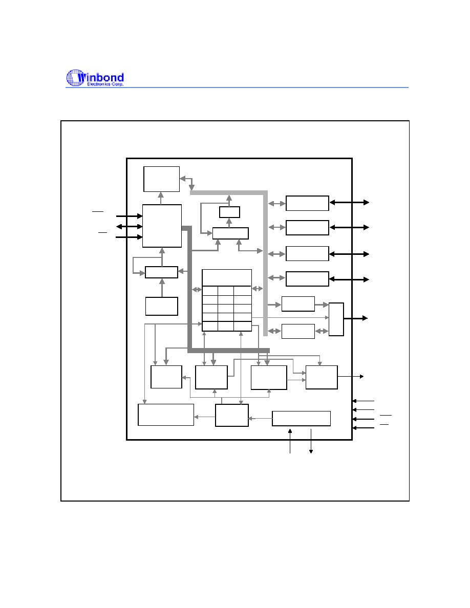
BLOCK DIAGRAM
XIN
XOUT
PC
STACK
(8 Levels)
RAM
(128*4)
ALU
Timer 0
(8-bit)
Timing Generator
PORT RA
PORT RB
Modulation
Frequency
Pulse
RA0 to 3
RB0 to 3
RE0 to 3
MFP
VDD
VSS
Flash
EEPROM
(2048*16)
(look_up table
2K*4)
Timer 1
(8-bit)
ACC
Divider 0
(14-bit)
Watchdog Timer
(4-bit)
HCF
PEF
HEF
IEF
Central Control
Unit
EVF
SEF
PSR0
.
.
MUX
SEL
+1(+2)
.
PORT RC
RC0 to 3
PORT RD
RD0 to 3
PR
PM0
MR0
PSR1 PSR2
PORT RT
Serial I/O
MUX
(RE0/DOUT,
RE1/CLKO,
RE2/DIN,
RE3/CLKI)
SEL
VPP (RES)
MODE (INT)
DATA (RA3)
RES
INT
Preliminary W541E20X
- 4 -
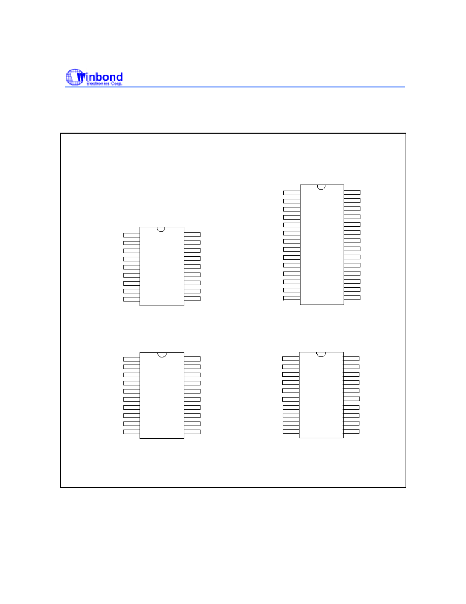
PIN CONFIGURATIONS
10
11
12
13
14
15
16
17
18
1
2
3
4
5
6
7
8
9
RB3
RB2
RB1
VSS
RA1
RA0
XIN
XOUT
VDD
RC3
RC2
RC1
(Vpp) /RES
(MODE) /INT
(DATA) RA3
RA2
RB0
RC0
RE3
RE2
RE1
VSS
RA1
RA0
XIN
XOUT
VDD
RD3
RD2
RD1
(Vpp) /RES
(MODE) /INT
(DATA) RA3
RA2
RE0
RD0
RB0
RC3
RB3
RB2
RB1
RC2
RC1
RC0
20
21
22
23
24
25
26
27
28
19
16
17
18
15
1
2
3
4
5
6
7
8
9
10
11
12
13
14
NC
MFP
W541E201
W541E202/W541E205
18-PDIP (300 mil)
28 SKINNY (300 mil), 28 SOP
10
11
12
13
15
16
17
18
1
2
3
4
5
6
7
8
9
RB3
RB2
RB1
VSS
RA1
RA0
XIN
XOUT
VDD
RC3
RC2
RC1
(Vpp) /RES
(MODE) /INT
(DATA) RA3
RA2
RB0
RC0
W541E203
20-PDIP (300 mil)
14
VSS
VDD
19
20
10
11
12
13
15
16
17
18
1
2
3
4
5
6
7
8
9
RB3
RB2
RB1
VSS
RA1
RA0
XIN
XOUT
VDD
RC3
RC2
RC1
(Vpp) /RES
(MODE) /INT
(DATA) RA3
RA2
RB0
RC0
W541E204
20 SOP
14
VSS
VDD
19
20

Preliminary W541E20X
Publication Release Date: June 2003
- 5 -
Revision A2
PIN DESCRIPTION
SYMBOL I/O
FUNCTION
XIN I
Input pin for oscillator.
Connected to crystal or resistor to generate system clock by code option.
External 10~20pF capacitor uses to get accurate freq in crystal mode.
XOUT O
Output pin for oscillator.
Connected to crystal or resistor to generate system clock by code option.
20pF capacitor is built in internal for crystal mode.
RA0
-
RA2,
RA3 (DATA)
I/O Input/Output
port.
Input/output mode specified by port mode 1 register (PM1). When used as
output port, can provide high sink current for driving LED.
RB0
-
RB3
I/O Input/Output
port.
Input/output mode specified by port mode 2 register (PM2). When used as
output port, can provide high sink current for driving LED.
RC0
-
RC3
I/O Input/Output
port.
Input/output mode specified by port mode 4 register (PM4). Each pin has
an independent interrupt capability in input mode.
RD0
-
RD3
I/O Input/Output
port.
Input/output mode specified by port mode 5 register (PM5).
RE0/DOUT,
RE1/CLKO,
RE2/DIN,
RE3/CLKI
I/O
Special input/output port.
This port can be configured by software to act as the output of internal
port RT or the serial I/O port. When used as output port, can provide high
sink current for driving LED.
MFP
O
Output pin only.
This pin can output modulating or nonmodulating frequency, or Timer 1
clock output specified by mode register 1 (MR1).
INT
(MODE)
1
I
External interrupt pin.
This pin must be tied to V
DD
through an external resistor. It is a low active
and floating input pin.
RES
(V
PP
)
1
I
System reset pin.
This pin must be tied to V
DD
through an external resistor when it is not
used to reset this chip. It is a low active and floating input pin.
V
DD
I
Positive power supply (+).
V
SS
I
Negative power supply (-).
Note: There are internal pull-high resistors in these pins of W741C20X.