
W541L250 Data Sheet
4-BIT MICROCONTROLLER
Publication Release Date: May 29, 2003
- 1 -
Revision A6
Table of Contents-
1.
GENERAL DESCRIPTION ......................................................................................................... 2
2.
FEATURES ................................................................................................................................. 2
3.
BLOCK DIAGRAM ...................................................................................................................... 4
4.
PIN CONFIGURATION............................................................................................................... 5
5.
PIN DESCRIPTION..................................................................................................................... 6
6.
ELECTRICAL CHARACTERISTICS........................................................................................... 7
6.1
Absolute Maximum Ratings .......................................................................................... 7
6.2
DC Characteristics ........................................................................................................ 7
6.3
AC Characteristics......................................................................................................... 8
7.
APPLICATION CIRCUIT............................................................................................................. 9
8.
REVISION HISTORY ................................................................................................................ 10

W541L250
- 2 -
1. GENERAL DESCRIPTION
The W541L250 is fully compatible with W741L250 in the terms of pin assignment and IC functon
except main oscillator. It is a high-performance 4-bit microcontroller (
�C) that provides an LCD driver.
The device contains a 4-bit ALU, two 8-bit timers, a divider, a 24
� 4 LCD driver, and five 4-bit I/O
ports (including 1 output port for LED driving). There are also five interrupt sources and 8-level
subroutine nesting for interrupt applications. The W541L250 operates on low voltage and very low
current and has two power reduction modes, hold mode and stop mode, which help to minimize power
dissipation.
The W541L250 is suitable for remote controllers, watches and clocks, multiple I/O products, keyboard
controllers, speech synthesis LSI controllers, and other products.
2. FEATURES
� Operating voltage: 1.2 ~ 1.8V (LCD drive voltage: 3.0V, or 4.5V)
� Single system clock
- Oscillation frequency up to 1 MHz , Crystal or RC oscillator is selected by mask code option ,
- High-frequency (400 KHz to 1 MHz) or low-frequency (32.768 KHz) oscillation is selected by
mask code option
� Memory
- 2048 � 16 bit program ROM (including 2K � 4 bit look-up table)
- 128 � 4 bit data RAM (including 16 working registers)
- 24 � 4 LCD data RAM
� 21 input/output pins
- Ports for input only: 2 ports/8 pins
- Input/output ports: 2 ports/8 pins
- Port for output only: 1 port /4 pins (high sink current to drive LEDs)
- MFP output pin: 1 pin (MFP)
- Do not be floating when it is as input or output open-drain (NMOS type).
� Power-down mode
- Hold function: no operation (except for oscillator)
- Stop function: no operation (including main clock)
� Five types of interrupts
- Three internal interrupts (Divider 0, Timer 0, Timer 1)
- Two external interrupt (Port RC and
INT
pin)

W541L250
Publication Release Date: May 29, 2003
- 3 -
Revision A6
� LCD driver output
- 24 segment � 4 common
- Static, 1/2 duty (1/2 bias), 1/3 duty (1/2 or 1/3 bias), 1/4 duty (1/3 bias) driving mode can be
selected
- LCD driver output pins can be used as DC output ports; selectable by code option
� MFP output pin
- Output is software selectable as modulating or nonmodulating frequency
- Works as frequency output specified by Timer 1
� Built-in 14-bit clock frequency divider circuit
� Two built-in 8-bit programmable countdown timers
- Timer 0: one of two internal clock frequencies (F
OSC
/4 or F
OSC
/1024) can be selected
- Timer 1: includes an auto-reload function; and one of two internal clock frequencies (F
OSC
or
F
OSC
/64) can be selected or falling edge of pin RC.0 can be selected (output through MFP pin)
� Built-in 18/14-bit watchdog timer selectable for system reset
� Powerful instruction set: 119 instructions
� 8-level subroutine (include interrupt) nesting
� Up to 4 �S instruction cycle (with 1 MHz operating frequency)
� Packaged in 64-pin QFP
W541L250
- 4 -
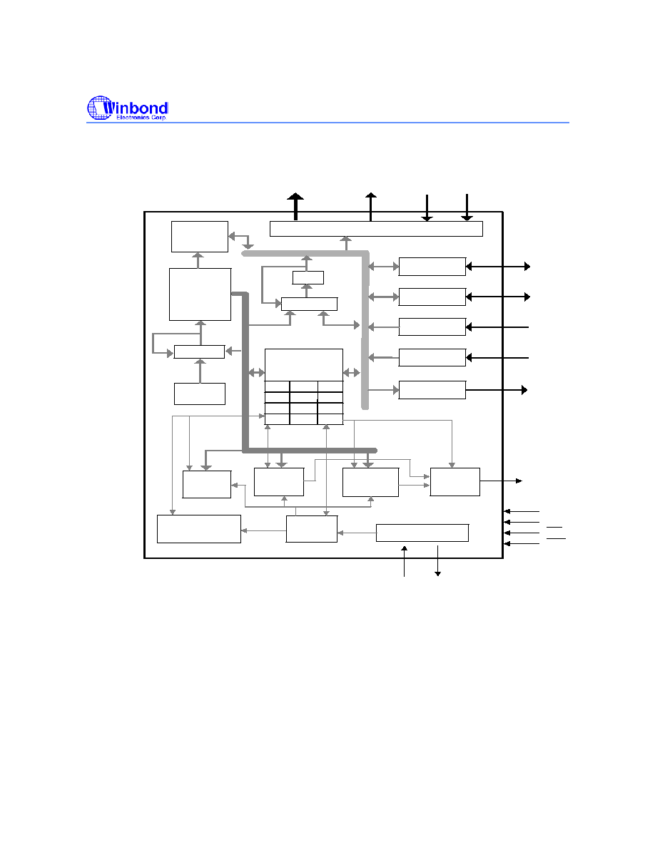
3. BLOCK DIAGRAM
LCD DRIVER
PC
STACK
(8 Levels)
RAM
(128*4)
ALU
Timer 0
(8 Bit)
Timing Generator
PORT RA
PORT RB
PORT RD
PORT RC
Modulation
Frequency
Pulse
SEG0 to SEG23
COM0 to COM3
RA0 to 3
RB0 to 3
RD0 to 3
RC0 to 3
RE0 to 3
MFP
XIN
XOUT
VDD
VSS
VDD1 to 3
DH1 to 2
ROM
(2048*16)
(look_up table
2K*4)
Timer 1
(8 Bit)
ACC
RES
INT
Divider 0
(14 Bit)
Watchdog Timer
(4 Bit)
HCF
PEF
HEF
IEF
Central Control
Unit
EVF
SEF
PSR0
PR
MR1
.
.
MUX
SEL
+1(+2)
PORT RE
.

W541L250
Publication Release Date: May 29, 2003
- 5 -
Revision A6
4. PIN CONFIGURATION
51 50 49 48 47 46 45 44 43 42 41 40 39 38 37 36 35 34 33
1 2 3 4 5 6 7 8 9 10 11 12 13 14 15 16 17 18 19
20
21
22
23
24
25
26
27
28
29
30
31
32
52
53
54
55
56
57
58
59
60
61
62
63
64
RD1
RD0
RC3
RC2
RC1
RC0
RB3
RB1
M
F
P
/
I
N
T
/
R
E
S
X
I
N
O
U
T
V
D N N
D C C
D
H
1
D
H
2
V
D
D
SEG18
SEG17
SEG16
SEG15
SEG14
SEG13
SEG12
SEG11
SEG10
R
E
2
R
E
3
V
S
S
N
C
N
C
C
O
M
C
O
M
C
O
M
C
O
M
S
E
G
S
E
G
S
E
G
S
E
G
S
E
G
S
E
G
3 2 1 0 0 1 2 3 4 5
R
D
D
E E
R R
R
2 3 0 1
S S S
E
E E
G G
E
G
2 1 0 9
G
SEG9
SEG8
SEG7
SEG6
RB0
RA3
RA2
RA1
RB2
S
2 2 2 1
S
E
G
3
2
3
V
D
D
2
V
D
D
X
R
A
0
1