
W551Cxxx Serial Voice Memory
Winbond Electronics Corp.
Release Date: January 2, 2001
Winbond W551Cxxx
Serial Voice Memory
Data Sheet

W551Cxxx Data Sheet
Winbond Electronics Corp.
Release Date: January 2, 2001
Contents
General Description
2
1.1 W551Cxxx Product Selection Guide ...................................................................................2
Features 3
2.1 W551Cxxx Features Description .........................................................................................3
2.2 W551Cxxx Pin Configuration & Description ......................................................................4
2.3 W551Cxxx System Block Diagram .....................................................................................5
Function Description
6
3.1 W551Cxxx Functional Description......................................................................................6
3.2 W551Cxxx Normal Read Mode...........................................................................................7
3.3 W551Cxxx Self-test Mode...................................................................................................8
Electrical Characteristics
9
4.1 W551Cxxx Absolute Maximum Ratings .............................................................................9
4.2 W551Cxxx DC Characteristics ............................................................................................9
4.3 W551Cxxx AC Characteristics ..........................................................................................10
Timing Waveform
11
5.1 W551Cxxx Timing Waveform...........................................................................................11
Applications 12
6.1 W551Cxxx Applications ....................................................................................................12
6.2 W551Cxxx Application Circuits ........................................................................................13
W551Cxxx Data Sheet
Winbond Electronics Corp.
2
Release Date: January 2, 2001
General Description
The W551Cxxx series is designated to interface with Winbond PowerSpeech
, BandDirector
, and
ViewTalk
family ICs directly. Application with PowerSpeech
, BandDirector
, and ViewTalk
the serial voice
memory W551Cxxx can lengthen the playback duration to meet the increasing market demand on complicated scenarios.
The W551Cxxx was already utilized the same serial interface as Winbond serial flash memory W55Fxx for designer to
simulate & verify the memory contents in advance. Besides that, W551Cxxx also provides a "Self-test mode" to verify
the voice memory contents easily and quickly.
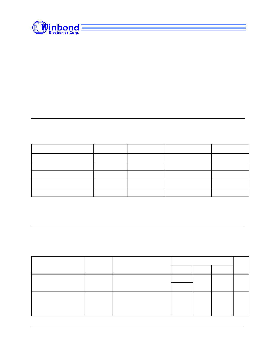
1.1 W551Cxxx Product Selection Guide
W551Cxxx Serial Voice Memory is used to store pre-determined data. To communicate with W551Cxxx in
serial data mode, the connection interface total pin counts can be reduced to three pins only. The following table is
shown the product selection guide of part number vs. memory density.
Part
#
W551C002 W551C005 W551C010 W551C020 W551C040 W551C060 W551C080
Density
256K bits
512K bits
1M bits
2M bits
4M bits
6M bits
8M bits

W551Cxxx Data Sheet
Winbond Electronics Corp.
3
Release Date: January 2, 2001
Features
2.1 W551Cxxx Features Description
!"
Wide range of operating voltage: 2.4V ~ 5.5V
!"
Operating frequency up to 1 MHz (@VDD = 2.4V)
!"
Versatile operation modes
#"Serial read mode
#"Serial check-sum output mode
#"Fast self-test mode
!"
Directly cascade for longer duration applications
!"
Serial shift-in address bus
!"
Serial data mode, the connection interface can be reduced to three pins:
#"CLK, ADDR, DATA
!"
Read access time: 500 ns
!"
Low power consumption
#"Operation current: 5 mA (typ.)
#"Standby current: 2 uA (typ.)
W551Cxxx Data Sheet
Winbond Electronics Corp.
4
Release Date: January 2, 2001
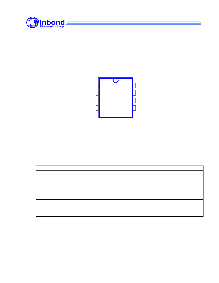
2.2 W551Cxxx Pin Configuration & Description
Pin Configuration
Pin Description
Pin Name
I/O
Description
TEST
I
Internal pulled high. Set TEST to low will enable "Self-test" function.
TEST_OUT
O
The output pin indicates the result of self-test process.
For correct result, a logic " 0 " signal will be output.
For incorrect result, a logic " 1 " signal will be output.
At Power-On-Reset condition, it outputs a logic " 1 " signal.
ADDR
I
Clock input for shift-in start address;
The first rising-edge signal will reset the address counter.
DATA
IO
Bi-directional data pin with the internal pull-high.
CLK
I
Clock input for data read-out.
VDD
Power Positive power supply pin.
VSS
Ground
TEST_OUT
NC
VSS
ADDR
TEST
VDD
CLK
DATA
1
2
3
4 5
6
7
8

W551Cxxx Data Sheet
Winbond Electronics Corp.
5
Release Date: January 2, 2001
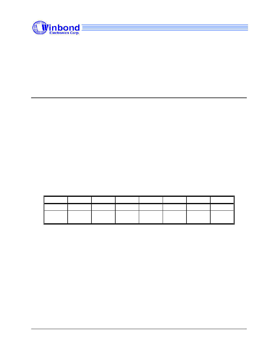
2.3 W551Cxxx System Block Diagram
Shit Register/
Address Counter
Decoder
Control
Page-Code
Comparator
Output
Buffer
Core
Array
POR
ADDR
DATA
CLK
TEST_OUT
TEST
W551Cxxx Data Sheet
Winbond Electronics Corp.
6
Release Date: January 2, 2001
Function Description
3.1 W551Cxxx Functional Description
The maximum number of the ADDR clock is 24 bits. The address data is shifted into the 24 bits address counter
by the ADDR clock. The MSB x bits of the address counter are the page codes, and the rest (24 - x) bits are the bit
of address. Note that the MSB is shifted first. The MSB 5 bits of the address counter are always gating (exclusive
OR) with the content of the page-code cells to determine whether these two articles are match or not. Only when the
page codes are matched with the content of the page-code cells, this device can be enabled. The counting source of
the address counter is the CLK clock, the falling edge signal of the CLK clock up-count the counter.
In normal-read mode the ADDR and CLK clock cannot be active simultaneously. The first rising edge signal of
the ADDR clock after CLK clocking will reset the address shift registers. The following table describes the needed
bits of
page code
:
Part
# W551C002 W551C005 W551C010 W551C020 W551C040 W551C060 W551C080
Density
256K bits
512K bits
1M bits
2M bits
4M bits
6M bits
8M bits
Bits of
page code
6 5 4 3 2 2 1

W551Cxxx Data Sheet
Winbond Electronics Corp.
7
Release Date: January 2, 2001
3.2 W551Cxxx Normal Read Mode
This chip can also be connected with Winbond PowerSpeech
, BandDirector
, and ViewTalk
TM
series
directly. Because in power-on condition, the default function mode is the normal read mode, then the mode selected
procedure can be skipped.
T
I
ADDR
DATA
CLK
TEST
� � �
� � �
24 bits
W551Cxxx Data Sheet
Winbond Electronics Corp.
8
Release Date: January 2, 2001
3.3 W551Cxxx Self-test Mode
In normal read mode, the TEST pin is internally pulled high, and the TEST_OUT pin is in logic ' 1 ' state.
When the TEST pin is pulled low, the W551Cxxx enters the "self-test mode". In this mode, the self-test process is
started at the falling edge of the TEST signal. The self-test process accumulates each byte (8 bit) of voice memory
content from address 00000h to 7FFFFh. If the accumulated result is 00h, a logic ' 0 ' will be output from
TEST_OUT pin. Or else, a logic ' 1 ' signal will be output from TEST_OUT pin.
TEST
TEST
_OUT
TEST
_OUT
T
TEST
For "Correct" result
For "Incorrect" result
End of test
W551Cxxx Data Sheet
Winbond Electronics Corp.
9
Release Date: January 2, 2001
Electrical Characteristics
4.1 W551Cxxx Absolute Maximum Ratings
PARAMETER SYMBOL
CONDITION
RATING UNIT
Operation Temperature
T
OPR
-
0 to +70
�
C
Storage Temperature
T
STG
-
-65 to +150
�
C
Power Supply (VDD-VSS)
V
DD
-V
SS
-
-0.3 to +7.0
V
Input D.C. Voltage
V
DC
All pins
-0.5 to Vcc+1.0
V
Transient Voltage (<20ns)
V
TRAN
All pins
-1.0 to Vcc+1.0
V
4.2 W551Cxxx DC Characteristics
V
DD
= 4.5V, TA = 25
�
C
LIMITS
PARAMETER SYMBOL
TEST
CONDITIONS
MIN. TYP. MAX.
UNIT
Operating Voltage
V
OP
-
2.4
(Note)
4.5 5.5 V
Operating Current
I
OP
In normal read mode, DATA,
TEST & TEST_OUT pins open;
f=1MHz
- 5 10
mA

W551Cxxx Data Sheet
Winbond Electronics Corp.
10
Release Date: January 2, 2001
Standby Current
I
SB
All inputs = GND;
DATA, TEST & TEST_OUT
pins open
- 1 2
uA
Input Leakage Current for
DATA
I
LI1
V
IN
= 0 V
-
-
-4.5
uA
Input Leakage Current for
TEST
I
LI2
V
IN
= 4.5 V
22.5
45
90
uA
Input Low Voltage
V
IL
All input pins
-0.3
-
0.8
V
Input High Voltage
V
IH
All input pins
2.0
-
VDD
V
Output Sink Current
I
OL
V
OL
= 0.5V
2.5
5
mA
Output Drive Current
I
OH
V
OH
= 4.0V
-2.5
-5
mA
ESD capability
V
ESD
- 2
-
-
KV
4.3 W551Cxxx AC Characteristics
VDD = 4.5V TA = 25
�
C
PARAMETER SYMBOL
CONDITION
MIN.
TYP.
MAX.
UNIT
Clock frequency of ADDR
F
ADDR
-
-
-
1
MHz
Clock frequency of CLK
F
CR
-
-
-
1 MHz
Interval time between ADDR and CLK
T
I
Read
mode
1 - - uS
Interval between DATA to another pin active
T
CFA
-
10 - - uS
Data access time
T
RA
Read
mode
-
- 500 nS
Data setup time
T
AS
Address
shift-in
250 -
-
nS
T
RH
Read
mode
0
-
-
nS
Data hold time
T
AH
Address
shift-in
10 - - nS
Self-test time
T
TEST
Self-test
mode
500
mS
W551Cxxx Data Sheet
Winbond Electronics Corp.
11
Release Date: January 2, 2001
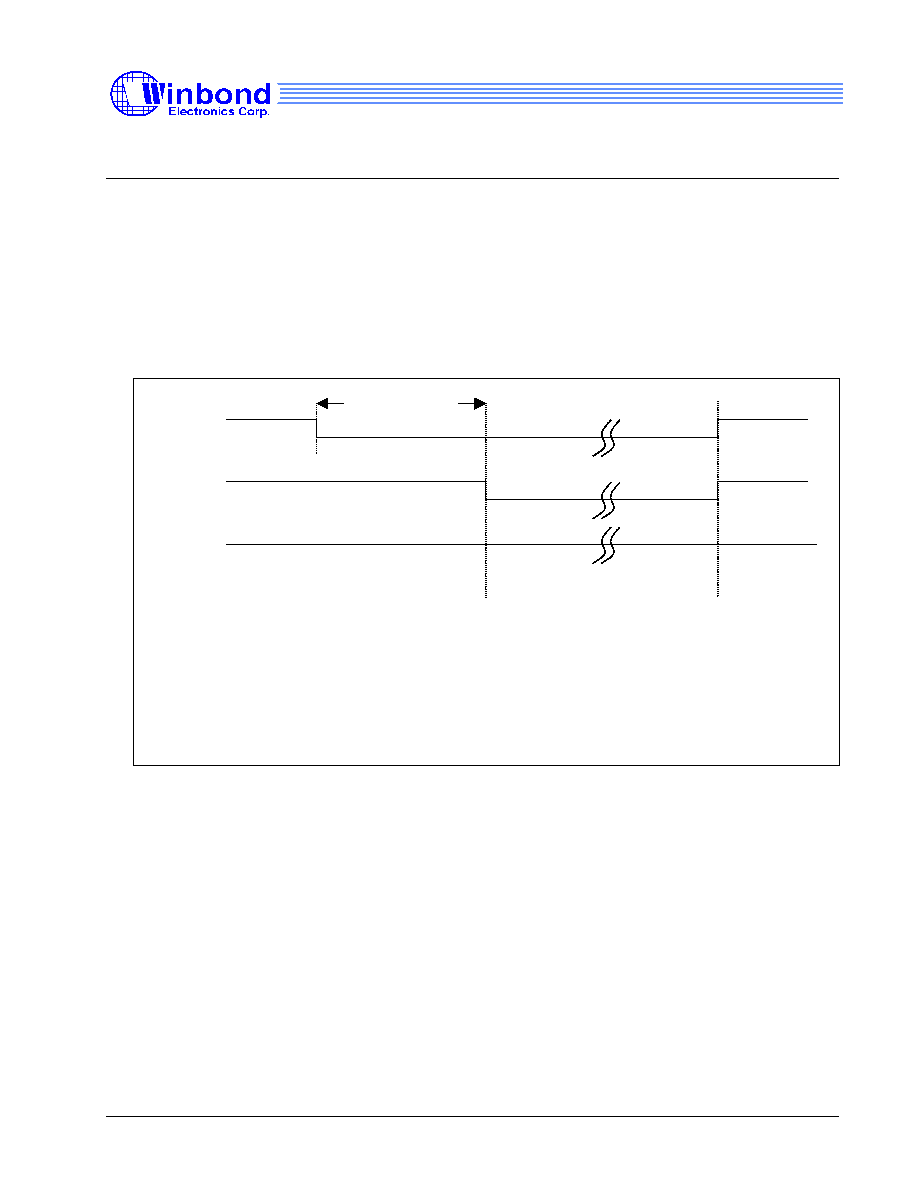
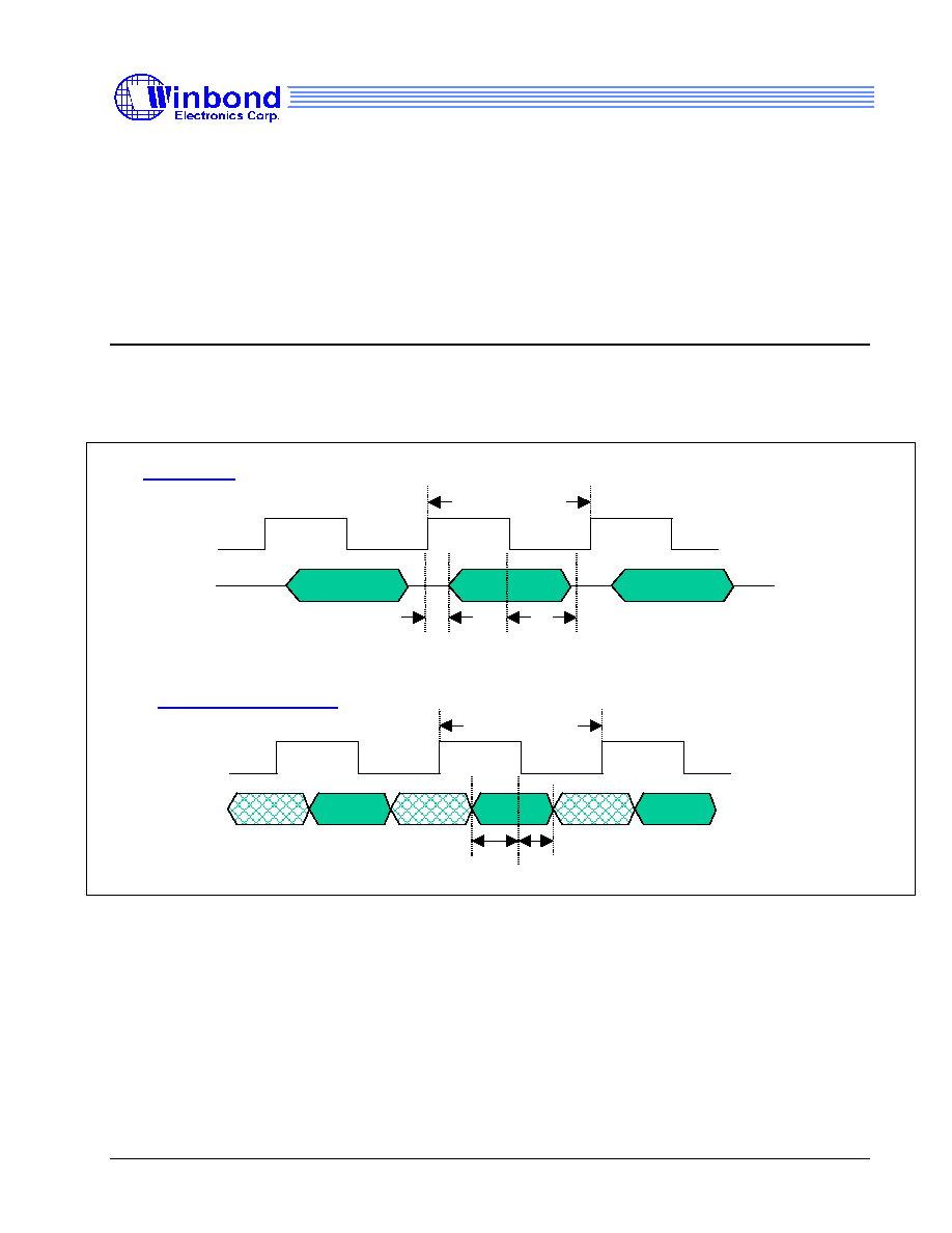
Timing Waveform
5.1 W551Cxxx Timing Waveform
1/F
CLK
CLK
Read Mode
T
RA
T
RH
DATA
1/F
CLK
ADDR
Address Shift-in Cycle
T
AS
T
AH
DATA
Note: The duty cycle of any clock is 50%

W551Cxxx Data Sheet
Winbond Electronics Corp.
12
Release Date: January 2, 2001
Applications
6.1 W551Cxxx Applications
W551Cxxx Applications for e-Book, e-Magazine, e-Novel, e-Story Book, or Hand-held Game

W551Cxxx Data Sheet
Winbond Electronics Corp.
13
Release Date: January 2, 2001
6.2 W551Cxxx Application Circuits
Application Circuits
(for reference only)
! With PowerSpeech
TM
, BandDirector
TM
, ViewTalk
TM
Applications
ADDR
DATA
CLK
W551Cxxx
ADDR
DATA
CLK
W58300/
W56000/
W536xxx
ADDR
DATA
CLK
! For Cascading Applications
W58300/
W56000/
W536xxx
ADDR
DATA
CLK
W551Cxxx
ADDR
DATA
CLK
W551Cxxx
ADDR
DATA
CLK
W551Cxxx

W551Cxxx Data Sheet
Winbond Electronics Corp.
14
Release Date: January 2, 2001
Headquarters
No. 4, Creation Rd. III,
Science-Based Industrial Park,
Hsinchu, Taiwan
TEL: 886-3-5770066
FAX: 886-3-5792697
http://www.winbond.com.tw/
Voice & Fax-on-demand: 886-2-27197006
Taipei Office
11F, No. 115, Sec. 3, Min-Sheng East Rd.,
Taipei, Taiwan
TEL: 886-2-27190505
FAX: 886-2-27197502
Winbond Electronics (H.K.) Ltd.
Rm. 803, World Trade Square, Tower II,
123 Hoi Bun Rd., Kwun Tong,
Kowloon, Hong Kong
TEL: 852-27513100
FAX: 852-27552064
Winbond Electronics North America Corp.
Winbond Memory Lab.
Winbond Microelectronics Corp.
Winbond Systems Lab.
2727 N. First Street, San Jose,
CA 95134, U.S.A.
TEL: 408-9436666
FAX: 408-5441798
Note: All data and specifications are subject to change without notice.