 | –≠–ª–µ–∫—Ç—Ä–æ–Ω–Ω—ã–π –∫–æ–º–ø–æ–Ω–µ–Ω—Ç: W55F10 | –°–∫–∞—á–∞—Ç—å:  PDF PDF  ZIP ZIP |
Document Outline
- Main Menu
- Speech Products
- Search
- Web

W55FXX
SERIAL FLASH EEPROM SERIES
Publication Release Date: August 1996
- 1 -
Revision A2
GENERAL DESCRIPTION
The W55FXX is a serial input/output flash EEPROM series that is typically used as the memory cell
of a W51300 (voice recorder controller) or the ROM code emulator for the PowerSpeech
TM
series.
The single voltage supply eliminates the need for an extra pump circuit during programming and
erasing.
FEATURES
∑
Provides CLK, ADDR, and DATA pins to operate with Winbond PowerSpeech
TM
series
∑
512K/1M/2M memory sizes available
∑
Directly cascadable for longer duration
∑
Fast frame-write operation
- Frame (32 bits) program cycle time: 400 µS (typ.)
∑
Fast whole-chip-erase duration: 50 mS (max.)
∑
Read data access time: 500 nS (max.)
∑
Program/erase cycles: 10,000 (typ.)
∑
Data retention: 10 years (typ.)
∑
Low power consumption:
- Operating: 5 mA (typ.)
- Standby: 2 µA (typ.)
PIN CONFIGURATION
MODE
EOP
CTRL
V
ADDR
DATA
CLK
V
1
8
2
3
4
5
6
7
SS
DD

W55FXX
- 2 -
PIN DESCRIPTION
NO.
PIN NAME
I/O
DESCRIPTION
1
EOP
O
End of process signal output
2
CTRL
I
Enable signal for program and erase operations when MODE = 0
Input clock for mode counter when MODE = 1
3
V
SS
I
Ground
4
ADDR
I
Input clock for start adress shift-in
5
DATA
I/O
Bidirectional data line
6
CLK
I
Input clock for data write-in and read-out
7
V
DD
I
Positive voltage supply
8
MODE
I
Mode select control pin
BLOCK DIAGRAM
ADDR
DATA
CLK
shift register
/address counter
Decoder
Write-in Buffer
Control
Circuit
CTRL
MODE
EOP
page-code cells
/page-code flag
/comparator
Output
Buffer
Core
Array
POR
Circuit
Pump
Circuit
W55FXX
Publication Release Date: August 1996
- 3 -
Revision A2
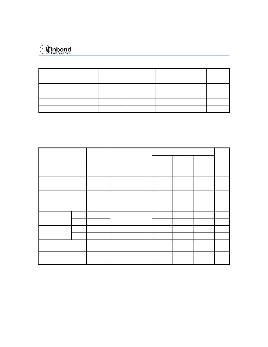
ABSOLUTE MAXIMUM RATINGS
PARAMETER
SYMBOL
CONDITION
RATED VALUE
UNIT
Operating Temp.
T
OPR
-
0 to +70
∞C
Storage Temp.
T
STG
-
-65 to +150
∞C
Power Supply
V
DD
-
V
SS
-
-0.3 to +7.0
V
Input DC Voltage
V
DC
All pins
-0.5 to V
DD
+1.0
V
Transient Voltage (< 20 nS)
V
TRAN
All pins
-1.0 to V
DD
+1.0
V
Note: Exposure to conditions beyond those listed under Absolute Maximum Ratings may adversely affect the life and reliability of the
device.
DC CHARACTERISTICS
(V
DD
= 4.5V, V
SS
= 0V, T
A
= 25
∞ C)
PARAMETER
SYMBOL
CONDITIONS
LIMITS
UNIT
MIN.
TYP.
MAX.
Operating voltage
V
DD
-
2.4
(Note)
4.5
5.5
V
Standby current
I
SB
All inputs = GND
DATA & EOP open
-
2
4
µA
Operating current
I
OP
In read mode
DATA & EOP open
F
OSC
= 1 MHz
-
5
10
mA
Input voltage
High
V
IH
All input pins
2.0
V
DD
V
Low
V
IL
-0.3
-
0.8
V
Output current
Sink
I
OL
V
OL
= 0.5V
2.5
5
-
mA
Drive
I
OH
V
OH
= 4.0V
-2.5
-5
-
mA
Input leakage current
of CTRL, MODE
I
LI1
V
IN
=
4.5V
-
-
4.5
µA
Input leakage current
of DATA
I
LI2
V
IN
= 0V
-
-
-4.5
µA
Note: For been working with W52900, the minimum operating voltage couldn't be less than 3.6 volt.
W55FXX
- 4 -
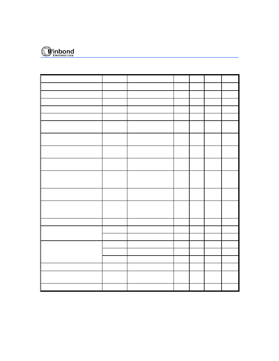
AC CHARACTERISTICS
(V
DD
= 4.5V, V
SS
= 0V, T
A
= 25
∞ C)
PARAMETER
SYMBOL
CONDITIONS
MIN.
TYP.
MAX.
UNIT
MODE pulse width
T
MP
-
1
-
-
µS
CTRL pulse width
T
WP
Page coding mode
400
-
700
µS
Clock frequency of ADDR
F
ADDR
-
-
-
1
MHz
Clock frequency of CLK
F
CLK
-
-
-
1
MHz
Clock frequency of CTRL
F
CTRL
-
-
-
1
MHz
Interval between ADDR end
& CLK begin
T
I
Read/Write mode
1
-
-
µS
Interval between CLK &
CTRL
T
GCC
Write mode
1
-
-
µS
Interval between ADDR &
CTRL
T
GCA
Page coding mode
1
-
-
µS
Interval between addressing
end & block-erase begin
T
AE
Block erase mode
1
-
-
µS
Interval between MODE
rising edge & CTRL clock
begin
T
MB
Mode selection
500
-
-
nS
Interval between CTRL clock
end & MODE falling edge
T
ME
Mode selection
500
-
-
nS
Interval between MODE
falling edge & another pin
active
T
GM
-
1
-
-
µS
Data access time
T
RA
Read mode
-
-
500
nS
Data set up time
T
WS
Write mode
250
-
-
nS
T
AS
-
250
-
-
nS
Data hold time
T
RH
Read mode
0
-
-
nS
T
WH
Write mode
10
-
-
nS
T
AH
-
10
-
-
nS
Programming duration
T
PR
Write mode
400
-
-
µS
Whole-chip-erase time
T
WE
Whole-chip-erase
mode
45
-
50
mS
Block-erase time
T
BE
Block-erase mode
40
-
45
mS
W55FXX
Publication Release Date: August 1996
- 5 -
Revision A2
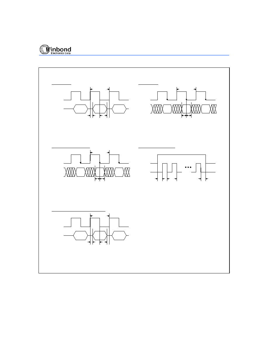
TIMING WAVEFORM
T
T
1/F
CLK
DATA
Write Cycle
T
T
1/F
CLK
DATA
Read Cycle
T
T
1/F
ADDR
DATA
Address Shift-in Cycle
T
T
MODE
CTRL
Mode Select Duration
1/F
T
T
1/F
CTRL
DATA
Page-code Cell Read Out Cycle
Note: The duty cycle of any clock is 50%.
CLK
RH
RA
WH
WS
ME
CTRL
MB
CLK
ADDR
AS
AH
CTRL
RH
RA