
W566Cxxx
4
S/3HQ/4T+2Per Speech+Melody Processor
(BandDirector
TM
Series)
GENERAL DESCRIPTION
The W566Cxxx is a powerful embedded microcontroller (uC) dedicated to speech and melody synthesis
applications. This series IC is tailored for plush toys, educational toys, or musical instruments. In multi-tasking
requirements, W566Cxxx series can make toy more funny than before. With the help of 16-bit microprocessor
(uP) W566-16, W566Cxxx can synthesize multi-channel speech and melody. 3-track of synthesized speech
can be in different kinds of format, for example ADPCM and MDPCM. Regarding synthesized melody,
W566Cxxx can provide 4-track of Tone melody (T-melody), or 3-track of
High-Quality melody (HQ-melody)
that
can emulate the characteristics of musical instruments. These signals can be mixed flexibly through 6-input
Mixer to produce colorful effects. The result of Mixer is converted to analog signal to drive speaker output.
W566Cxxx has two kinds of power saving modes: one is HOLD mode and the other is STOP mode. In
HOLD mode, the specific peripherals can be inactivated and IC can operate at the sub-clock. Consequently,
the W566Cxxx can perform some special tasks periodically. In STOP mode, all the IC's peripherals are
disable which is designated specially for try-me application. Besides, W566Cxxx can sink 8mA at most for
high-current application.
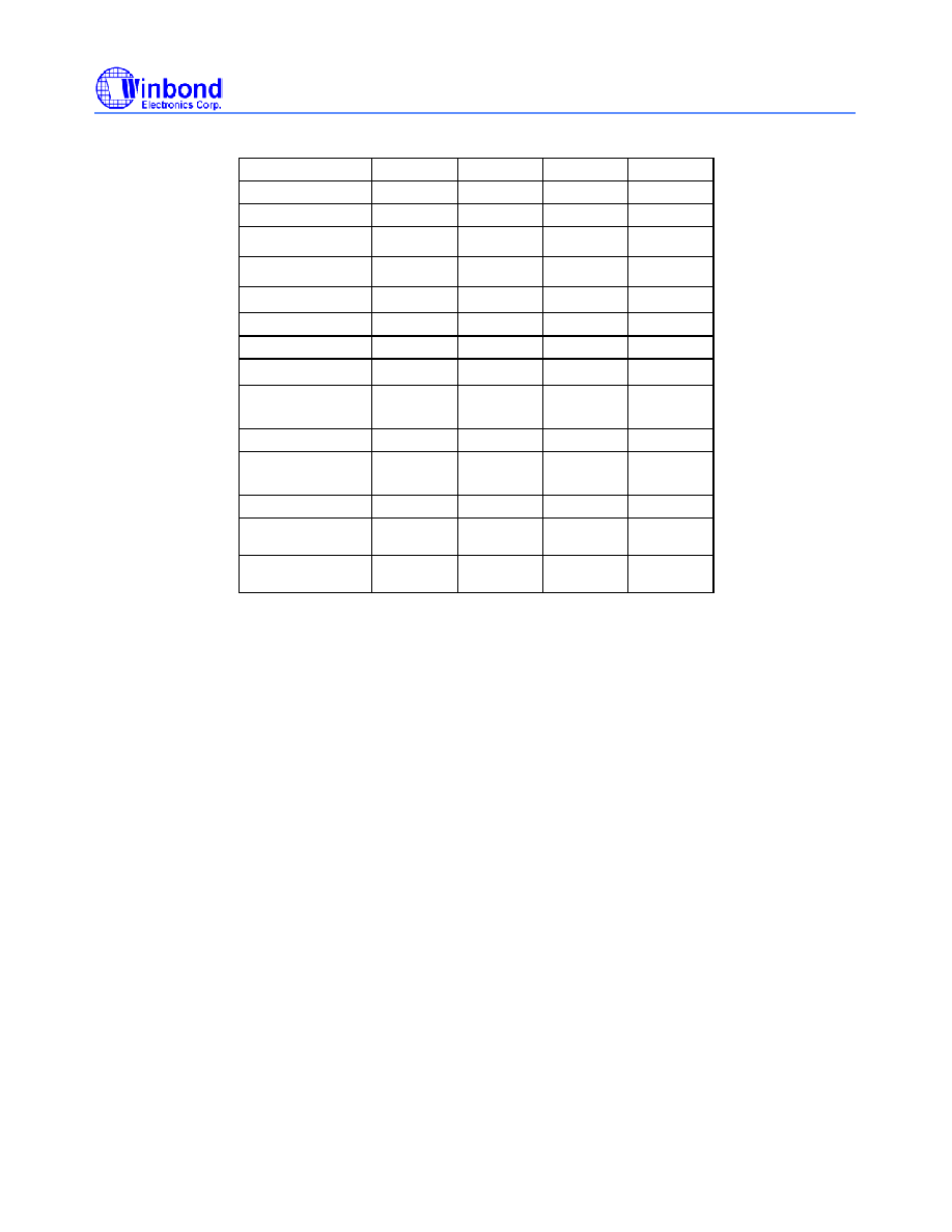
The characteristics of W566Cxxx series are depicted in the following table.
Publication Release Date: October 2001
-
1 -
Revision A5
W566Cxxx
Part Number
W566C210
W566C260 W566C300
W566C340
ROM (byte)
650K 792K 922K 1020K
RAM (byte)
512 512 512 512
Duration1 (sec)
*
212" 260" 304" 338"
Duration2 (sec)
*
159" 195" 228" 253"
In : Bid
1
8:16 8:16 8:16 8:16
Speaker Driver
DAC DAC DAC DAC
Mixer Inputs
6 6 6 6
Speech Tracks
2
4 4 4 4
Speech Algorithms
ADPCM
MDPCM
PCM
ADPCM
MDPCM
PCM
ADPCM
MDPCM
PCM
ADPCM
MDPCM
PCM
Melody Tracks
3 3 3 3
Instrument Types
HQ
Tone
Voice
HQ
Tone
Voice
HQ
Tone
Voice
HQ
Tone
Voice
IR-Carrier
Numbers of System
Clock
2 2 2 2
Power
Management
HOLD
STOP
HOLD
STOP
HOLD
STOP
HOLD
STOP
*The Duration1 is calculated based on 6000Hz*4-bits=24Kbps, 24Kbps on the
assumption that all the ROM space is used to store speech data.
*The Duration2 is calculated based on 8000Hz*4-bits=32Kbps, 32Kbps on the
assumption that all the ROM space is used to store speech data.
1
"In" is the number of input pins; "Bid" is the number of I/O pins.
2
Synthesized speech in ADPCM/MDPCM format.
Publication Release Date: October 2001
-
2 -
Revision A5

W566Cxxx
FEATURES
� Wide range of operating voltage:
4 M Hz @ 2.4 volt ~ 5.5 volt
6 M Hz @ 3.6 volt ~ 5.5 volt
� Sophisticated power management:
- dual system clocks, one in 6M Hz and the other in 32768 Hz
- HOLD mode for dealing with interrupt events only
- STOP mode for stopping all IC operations
� 8 input pins
� 16 I/O pins and 8 of them can sink 8mA in their output portion
� Versatile Digital-to-Analog Converter (DAC) to drive speaker output:
- 10-bit Current type DAC (DAC) with programmable output current
� Multiple synthesized speech formats: ADPCM/MDPCM/PCM
� 3 tracks synthesized ADPCM/MDPCM speech at programmable playback rate
� 4 tracks Tone melody that can emulate envelope of musical instruments
� 3 tracks
High-Quality melody
that can emulate characteristic of musical instruments
� 6-input/10-bit-resolution Mixer can mix the speech and melody signals flexibly
� Built-in IR carrier generation circuit for simplification firmware IR application
� Built-in 6 timers for speech/melody synthesis and general purpose applications
� Built-in Watch-Dog Timer (WDT)
� Built-in Divider for real-time clock application
� Available package: COB
Publication Release Date: October 2001
-
3 -
Revision A5
W566Cxxx
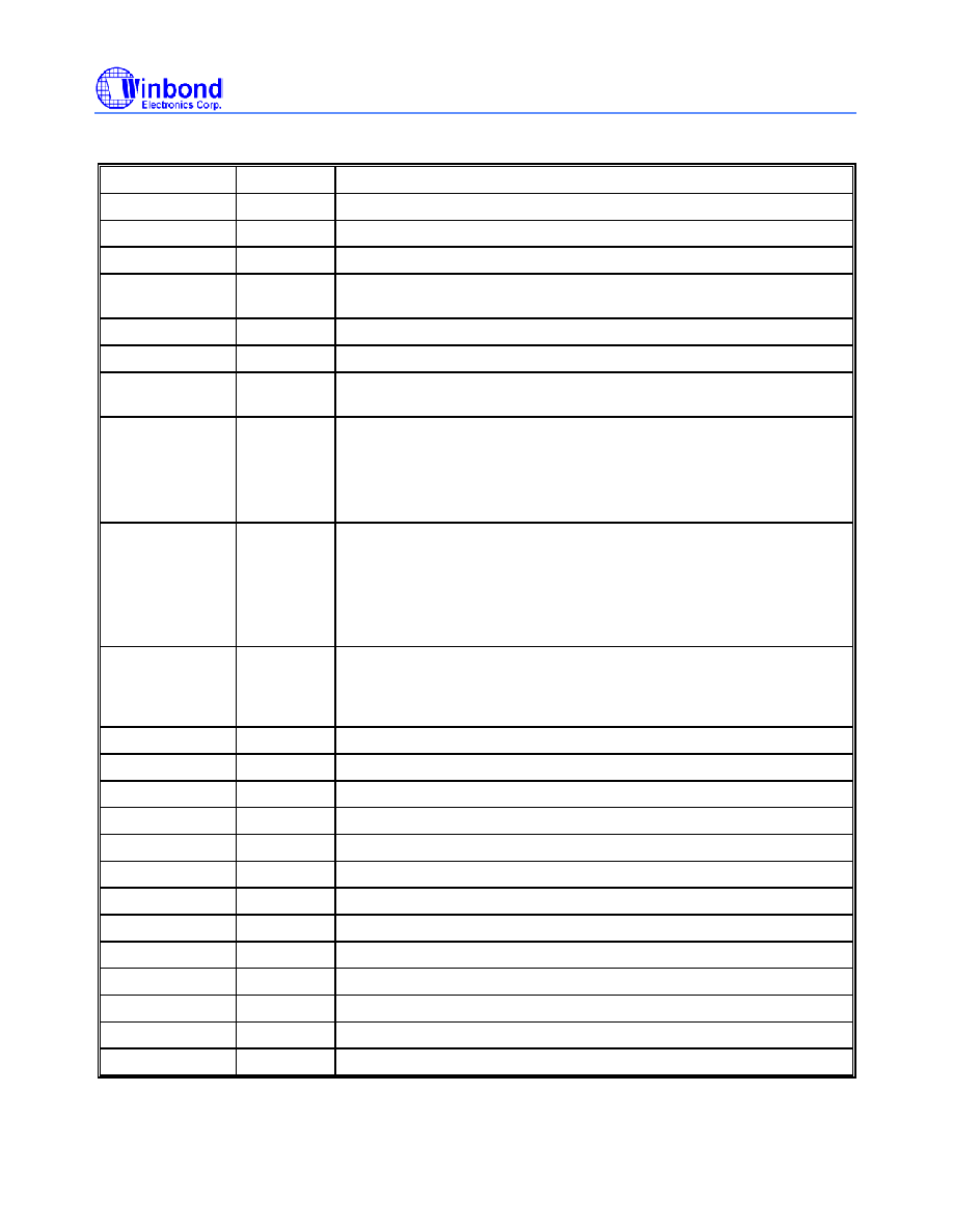
PIN DESCRIPTION
PIN NAME
I/O
FUNCTION
RESETB
In
IC reset input.
XIN
In
Sub-clock oscillation input.
XOUT
Out
Sub-clock oscillation output.
XSEL
In
Pin selection of sub-clock type. When XSEL is logic 1, RC type is used.
When XSEL is logic 0, crystal type is used.
OSCI
In
Main-clock oscillation input.
OSCO
Out
Main-clock oscillation output.
OSCSEL
In
Pin selection of main-clock type. When OSCSEL is logic 1, Ring type is
used. When OSCSEL is logic 0, crystal type is used.
IP0[7:0]
In
General input port with pull-high selection. Each input pin can be
programmed to generate interrupt request and used to release IC from
HOLD/STOP mode.
IP0.6 can be used as the external clock source of the general timer
TimerG.
BP0[7:0]
I/O
General input/output pins. When used as output pin, it can be open�
drain or CMOS type and it can sink 8mA for high-current application.
When used as input pin, there may have a pull-high option and generate
interrupt request to release IC from HOLD/STOP mode.
When BP0[7] is used as output pin, it can be the IR transmission carrier
for firmware IR application.
BP1[7:0]
I/O
General input/output pins. When used as output pin, it can be open�
drain or CMOS type. When used as input pin, there may have a pull-high
option and generate interrupt request to release IC from HOLD/STOP
mode.
DAC+
Out
Current type DAC
NC_DAC2
Out
Reserved, non connect
NC_SPK1
Out
Reserved, non connect
NC_SPK2
Out
Reserved, non connect
TEST
In
Test input. Do not connect during normal operation.
VDD
Power
Positive power supply for uP.
VSS
Power
Negative power supply for uP.
VDD1
Power
Positive power supply for peripherals.
VSS1
Power
Negative power supply for peripherals.
OVDD
Power
Positive power supply for oscillation.
OVSS
Power
Negative power supply for oscillation.
PVDD
Power
Positive power supply for speaker output.
PVSS
Power
Negative power supply for speaker output.
Publication Release Date: October 2001
-
4 -
Revision A5
W566Cxxx
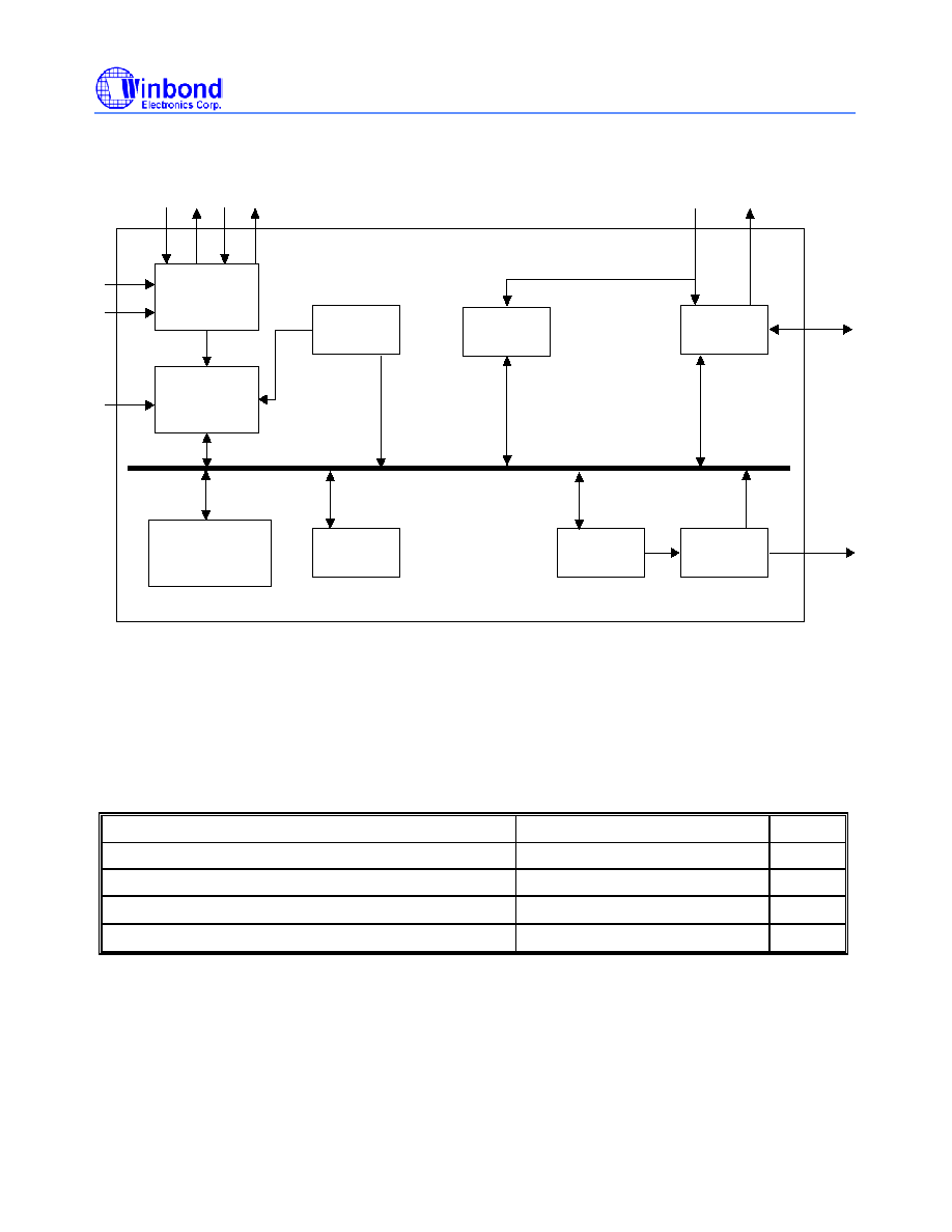
BLOCK DIAGRAM
Timing
Generator
16 bits uP
Data RAM
Program ROM
Speaker
Driver
Interrupt
Controller
6 Timers
I/O
WDT
Divider
Mixer
Address/Data Bus
OSCO
OSCI
XIN
XSEL
OSCSEL
XOUT
IP[7:0]
IP0[6]
BP1[7:0]
BP0[7:0]
DAC+
RESETB
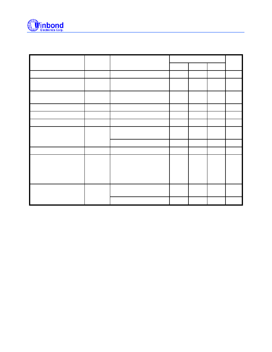
ABSOLUTE MAXIMUM RATINGS
PARAMETER RATING
UNIT
Supply Voltage to Ground Potential
-0.3 to +7.0
V
D.C. Voltage on Any Pin to Ground Potential
-0.3 to VDD+0.3
V
Operating Temperature
0 to +70
�C
Storage Temperature
-55 to +150
�C
Note: Exposure to conditions beyond those listed under Absolute Maximum Ratings may adversely affect the
life and reliability of the device.
Publication Release Date: October 2001
-
5 -
Revision A5
W566Cxxx
D.C. ELECTRICAL CHARACTERISTICS
(V
DD
-V
SS
= 4.5 V, F
M
=6 MHz, F
S
=32768 Hz, Ta= 25
�C; No Load unless otherwise specified)
SPEC.
PARAMETER SYMBOL
TEST
CONDITIONS
Min. Typ. Max.
UNIT
Operating Voltage
V
DD
F
SYS
= 6 MHz
3.6
--
5.5
V
Operating Current
I
OP
F
SYS
=F
M
, F
S
active, normal
operation
-- -- 12
mA
Hold Current
I
HD
F
SYS
=F
S
, F
M
inactive, HOLD
mode
-- -- 25
uA
Standby Current
I
SB
STOP
mode
-- -- 1 uA
Input Low Voltage
V
IL
All input pins
V
SS
--
0.3V
DD
V
Input High Voltage
V
IH
All input pins
0.7V
DD
-- V
DD
V
Vout=0.4V, all output pins
expect BP0
-- -- 4
mA
Output Low Current
I
OL
Vout=0.4V, BP0 only
--
--
8
mA
Output High Current
I
OH
Vout=2.4V, all output pins
-4
--
--
mA
DAC Full Scale Current
I
DAC
VDD=4.5V, RL=100
-1.6
-2.4
-3.2
-4.0
-2.0
-3.0
-4.0
-5.0
-2.4
-3.6
-4.8
-6.0
mA
All input pins except
RESETB
160 -- 300
K
Pull High Resistance
R
IN
RESERB 100
--
--
K
Publication Release Date: October 2001
-
6 -
Revision A5
W566Cxxx
A.C. ELECTRICAL CHARACTERISTICS
(V
DD
-V
SS
= 4.5 V, F
M
=6 MHz, F
S
=32768 Hz, Ta= 25
�C; No Load unless otherwise specified)
SPEC.
PARAMETER SYMBOL
TEST
CONDITIONS
Min. Typ. Max.
UNIT
Ring type, R= 370 K
5.7 6 6.3
MHz
Main-Clock F
M
Crystal
type
-- 6 --
MHz
RC type, R= 1650 K
26.214 32.768 39.322 KHz
Sub-Clock
F
S
Crystal
type
-- 32.768 -- Hz
Cycle Time
T
CYC
F
SYS
= 6 MHz
167
--
DC
ns
Ring type, R= 370 K
-- 3 5
ms
Main-Clock Wake-up
Stable Time
T
WSM
Crystal type, F
M
= 6 MHz
--
3
5
ms
RC type, R= 1650 K
-- 1 2 s
Sub-Clock Wake-up
Stable Time
T
WSS
Crystal type, F
S
=32768 Hz
--
1
2
s
Main-Clock Frequency
Deviation, Ring type
F
F
1
MIN
MIN
MAX
F
F
-
F
-- 3 5 %
RESETB Active Width
T
RES
After
F
SYS
stable
4
T
CYC
STABILITY DATA
� Resistance vs. Frequency for W566C340 at V
DD
= 4.5V, main-clock in Ring Type
� Resistance vs. Frequency for W566C340 at V
DD
= 4.5V, sub-clock in RC Type
1
"F
MAX
" is max oscillation frequency for operating voltage V
DD
, "F
MIN
" is minimum oscillation frequency for
operating voltage V
DD
Publication Release Date: October 2001
-
7 -
Revision A5
W566Cxxx
APPLICATION CIRCUITS
� F
M
connection
OVDD
W566C
OSCI
OSCO
OSCSEL
Ring type
OVSS
W566C
OSCI
OSCO
OSCSEL
Crystal type
� F
S
connection
OVDD
W566C
XIN
XOUT
XSEL
RC type
OVSS
W566C
XIN
XOUT
XSEL
Crystal type
Publication Release Date: October 2001
-
8 -
Revision A5
W566Cxxx
� Speaker output connection
W566C
DAC+
PVDD
PVSS
Current type
speaker output
� IR Tx/Rx connection
W566C
BP0[7]
IP0[7]
LTM97AS
3 2 1
BP0[0]
VSS1
VDD1
VSS1
Publication Release Date: October 2001
-
9 -
Revision A5

W566Cxxx
Headquarters
No. 4, Creation Rd. III,
Science-Based Industrial Park,
Hsinchu, Taiwan
TEL: 886-3-5770066
FAX: 886-3-5792697
http://www.winbond.com.tw/
Voice & Fax-on-demand: 886-2-27197006
Taipei Office
11F, No. 115, Sec. 3, Min-Sheng East Rd.,
Taipei, Taiwan
TEL: 886-2-27190505
FAX: 886-2-27197502
Winbond Electronics (H.K.) Ltd.
Rm. 803, World Trade Square, Tower II,
123 Hoi Bun Rd., Kwun Tong,
Kowloon, Hong Kong
TEL: 852-27513100
FAX: 852-27552064
Winbond Electronics North America Corp.
Winbond Memory Lab.
Winbond Microelectronics Corp.
Winbond Systems Lab.
2727 N. First Street, San Jose,
CA 95134, U.S.A.
TEL: 408-9436666
FAX: 408-5441798
Note: All data and specifications are subject to change without notice.
Publication Release Date: October 2001
-
10 -
Revision A5