
W567SXXX Data Sheet
8-CHANNEL SPEECH+MELODY PROCESSOR
(BandDirector
TM
Series)
Publication Release Date: October 15, 2003
- 1 -
Revision A8
Table of Contents-
1.
GENERAL DESCRIPTION ......................................................................................................... 2
2.
FEATURES ................................................................................................................................. 3
3.
PIN DESCRIPTION..................................................................................................................... 4
4.
BLOCK DIAGRAM ...................................................................................................................... 5
5.
ELECTRICAL CHARACTERISTICS........................................................................................... 5
5.1
Absolute Maximum Ratings............................................................................................... 5
5.2
DC Characteristics............................................................................................................. 6
5.3
AC Characteristics............................................................................................................. 7
6.
TYPICAL APPLICATION CIRCUIT............................................................................................. 8
7.
REVISION HISTORY .................................................................................................................. 9
W567SXXX
- 2 -
1. GENERAL DESCRIPTION
The W567Sxxx is a powerful microcontroller (uC) dedicated to speech and melody synthesis
applications. With the help of the embedded 8-bit microprocessor & dedicated H/W, the W567Sxxx
can synthesize 8-channel speech+melody simultaneously.
The two channels of synthesized speech can be in different kinds of format, for example ADPCM and
MDPCM. The W567Sxxx can provide 8-channel high-quality WinMelody
TM
, which can emulate the
characteristics of musical instruments, such as piano and violin. The output of speech/melody
channels are mixed together through the on-chip digital mixer to produce colorful effects. The mixer is
further processed to drive dual speakers with stereo effects. With these hardware resources, the
W567Sxxx is very suitable for high-quality and sophisticated scenario applications.
The W567Sxxx is also capable of transmitting infrared (IR) signals with on-chip carrier generator. As a
result, toys can be designed to interact with each other for more play values. A serial interface can be
supported as external memory for memory expansion or content-updateable applications.
Besides, the W567Sxxx is equipped with a 4-channel Analog-to-Digital Converter (ADC). With ADC, a
toy can respond to environment conditions such as temperature or pressure via sensory devices.
Therefore, toys with ADC can behave vividly than ever before.
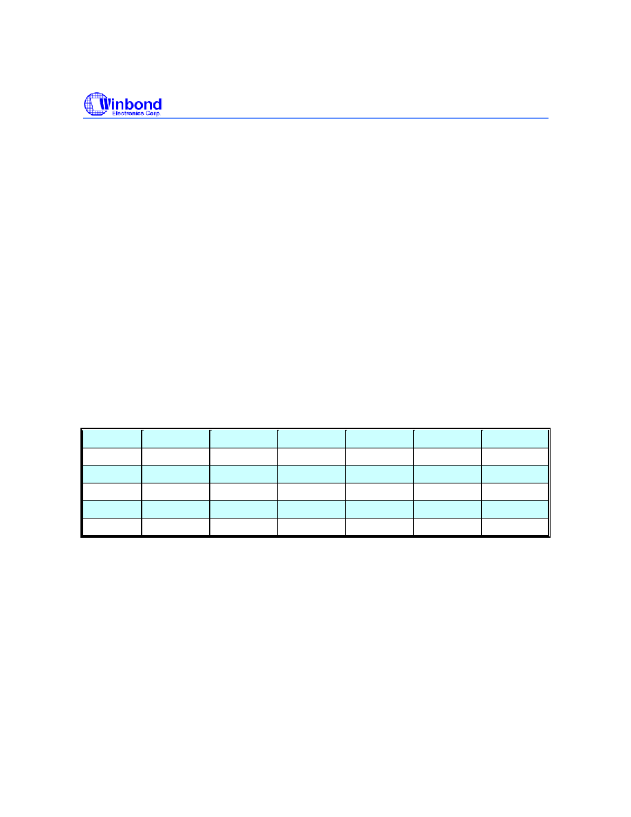
The W567Sxxx family contains several items with different playback duration as shown below: (@5-bit
MDPCM algorithm, 6 KHz sampling rate)
Item
W567S010
W567S015
W567S020
W567S025
W567S030
W567S040
*Duration
14 sec.
18 sec.
27 sec.
31 sec.
35 sec.
52 sec.
Item
W567S060
W567S080
W567S100
W567S120
W567S150
W567S170
Duration
60 sec.
104 sec.
116 sec.
129 sec.
163 sec.
197 sec.
Item
W567S210
W567S260
W567S301
W567S341
Duration
232 sec.
265 sec.
300 sec.
334 sec.
Note:
*: The duration time is based on 5-bit MDPCM at 6 KHz sampling rate. The firmware library and timber library have been
xcluded from user's ROM space for the duration estimation.

W567SXXX
Publication Release Date: October 15, 2003
- 3 -
Revision A8
2. FEATURES
� Wide range of operating voltage:
- 8 MHz @ 3.6 volt ~ 5.5 volt
- 4 MHz @ 2.4 volt ~ 5.5 volt
� Power
management:
- 4 ~ 8 MHz system clocks, with Ring type
- Stop mode for stopping all IC operations
� Provides up to 8 inputs and 24 I/O pins
� Current-type
Digital-to-Analog Converter (DAC):
- 8-bit resolution with programmable output current
- 2 speaker outputs for stereo applications
� F/W speech synthesis with multiple format support: ADPCM/MDPCM/PCM
� 2 speech synthesis
1
channels at programmable sample rate
� 8 melody channels that can emulate characteristics of musical instruments
� 8-input/10-bit-resolution Mixer can mix the speech and melody signals flexibly
� Dynamic control of the channel assignment to the dual speaker output for stereo effects
� Built-in IR carrier generation circuit for simplifying firmware IR application
� 4-channel ADC interface (W567S301~S341) with maximum 4-KHz sampling rate and 6-bit
effective resolution
� Built-in 9 timers for speech/melody synthesis and general purpose applications
� Built-in 10*7 multiplier
� Built-in Watch-Dog Timer (WDT) and Low Voltage Detect (LVD)
� Built-in 32KHz crystal oscillator with divider for time-keeping application in W567S080 ~ S341
� Built-in Serial Interface Manager (SIM) in W567S080 ~ S341
� Support PowerScript for developing codes in easy way
� Full-fledged development system
- Source-level ICE debugger
- Event synchronization mechanism
- Compatible with W566B/C & W588S system
- User-friendly GUI environment
� Available package form: (COB is essential)
- W567S010, S015, S020, S025, S030: LQFP48
- W567S040, S060: QFP64
- W567S080 ~ S120: LQFP80
- W567S150 ~ S341: LQFP100
1
More speech channels are available for 8-bit PCM format in the remaining melody channels.
W567SXXX
- 4 -
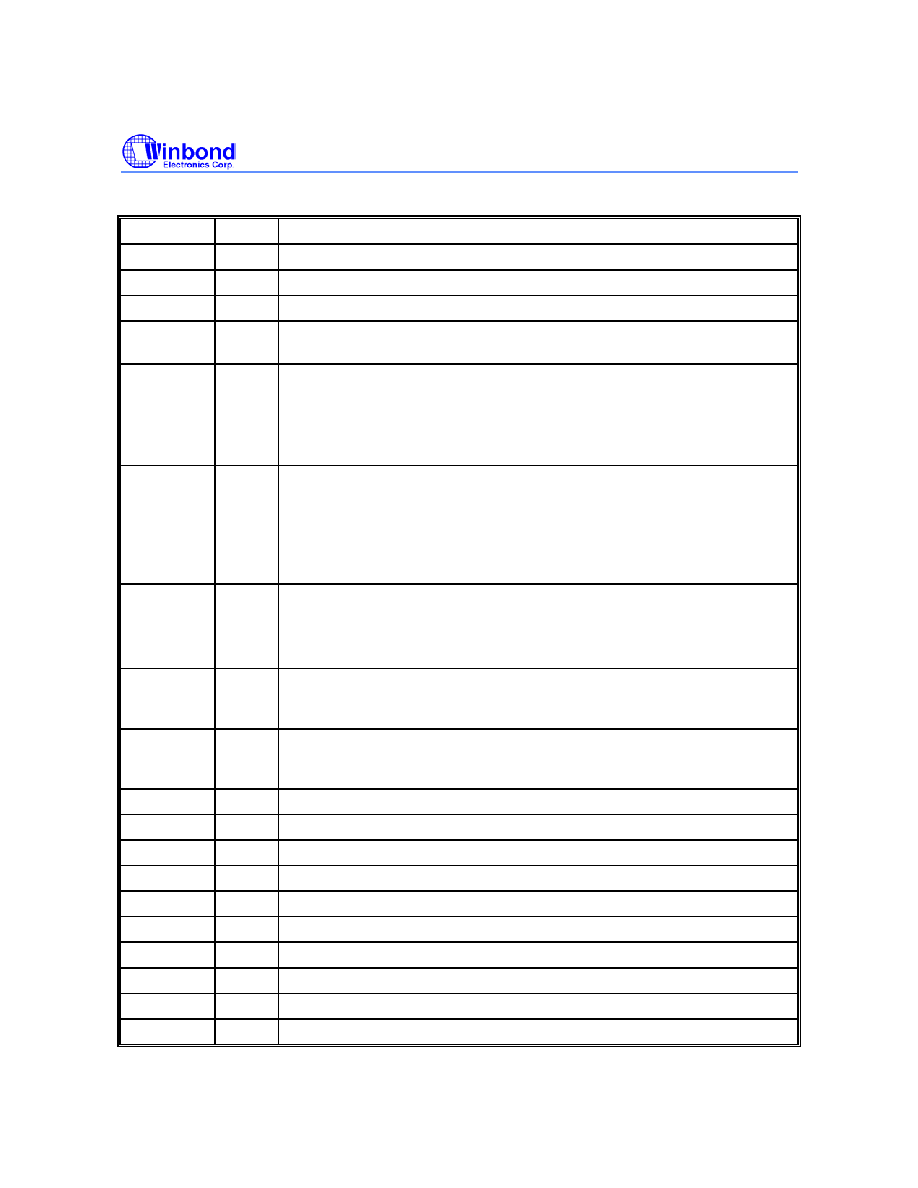
3. PIN DESCRIPTION
PIN NAME
I/O
FUNCTION
RESETB
In
IC reset input, low active.
XIN
In
32 KHz crystal oscillator with divider for time-keeping application
XOUT
Out
32 KHz crystal oscillator with divider for time-keeping application
OSC In
Main-clock oscillation input. Only Ring type is used. Connect to GND via the
oscillation resistor.
IP0[3:0] /
IP0[7:4]
In
General input port with pull-high selection. Each 2 input pins can be
programmed to generate interrupt request and used to release IC from
STOP mode.
IP0[3:0] are used as the input of ADC. IP0.0 is the input pin of channel 0
and IP0.3 is the input pin of channel 3, and so on.
BP0[7:0] I/O
General input/output pins. When used as output pin, it can be open�drain
or CMOS type and it can sink 8mA for high-current applications. When
used as input pin, there may have a pull-high option and generate interrupt
request to release IC from STOP mode.
When BP0[7] is used as output pin, it can be the IR transmission carrier for
IR applications.
BP1[7:0]
I/O
General input/output pins. When used as output pin, it can be open�drain
or CMOS type. When used as input pin, there may have a pull-high option
and generate interrupt request to release IC from STOP mode.
When serial interface is enabled, BP1[6:4] are used as serial interface pins.
BP2[7:0]
I/O
General input/output pins. When used as output pin, it can be open�drain
or CMOS type. When used as input pin, there may have a pull-high option
and generate interrupt request to release IC from STOP mode.
*VRB Out
Reference-bottom voltage of ADC. Theoretically, the converted codes 0 ~
255 will be uniformly distributed between VRB and AVDD. Voltages below
VRB will be mapped to code 0.
*CIN
In
Capacitor input for ADC.
*COUT
Out
Capacitor output for ADC.
*AV
DD
Out
ADC regulator output voltage.
DAC0
Out
Current type DAC speaker output 0.
DAC1
Out
Current type DAC speaker output 1.
TEST
In
Test input, internally pulled low. Do not connect during normal operation.
V
DD
(V
DD1
)
Power Positive power supply.
V
SS
(V
SS1
)
Power Negative power supply.
*V
DDA
Power Positive power supply for ADC module.
*V
SSA
Power Negative power supply for ADC module.
*: Only W567S301~S341 provides these pins for ADC application.
W567SXXX
Publication Release Date: October 15, 2003
- 5 -
Revision A8
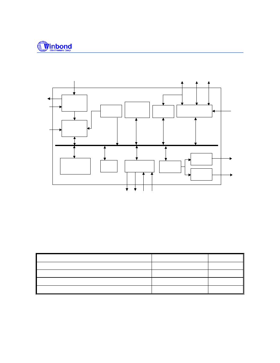
4. BLOCK DIAGRAM
Timing
Generator
8 bits uP
Data RAM
Program ROM
Speaker
Driver
Interrupt
Controller
Timers
&
HQ generator
I/O
WDT
4 Channels
ADC
Mixer
Address/Data Bus
OSC
BP1[7:0]
DAC0
RESETB
Speaker
Driver
DAC1
IP0[3:0]
or
IP0[7:4]
XIN
XOUT
Serial
Interface
BP1[6:4]
VRB
CIN IP0[3:0]
COUT
BP2[7:0]
BP0[7:0]
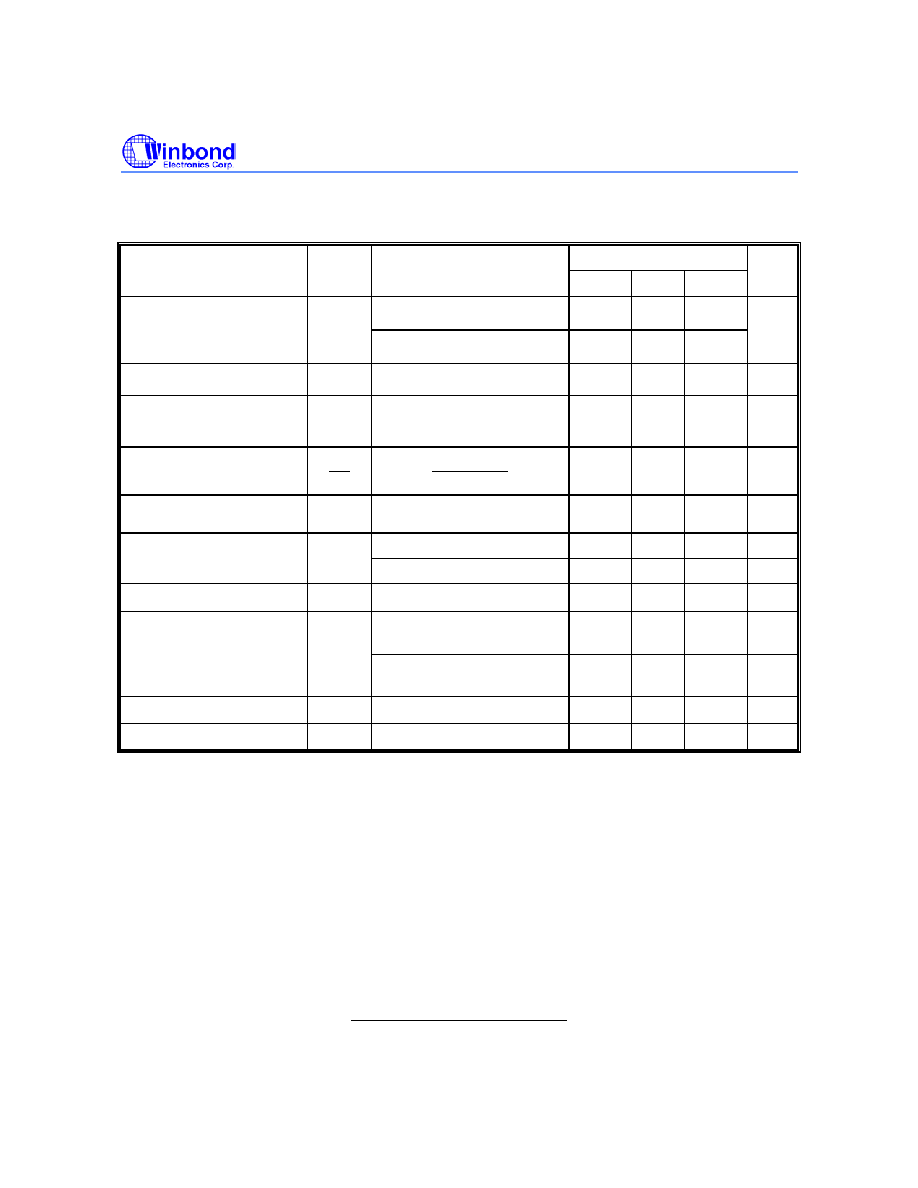
5. ELECTRICAL CHARACTERISTICS
5.1 Absolute Maximum Ratings
PARAMETER RATING
UNIT
Supply Voltage to Ground Potential
-0.3 to +7.0
V
D.C. Voltage on Any Pin to Ground Potential
-0.3 to V
DD
+0.3
V
Operating Temperature
0 to +70
�C
Storage Temperature
-55 to +150
�C
Note: Exposure to conditions beyond those listed under Absolute Maximum Ratings may adversely affect the life and reliability
of the device.

W567SXXX
- 6 -
5.2 DC Characteristics
(V
DD
-V
SS
= 4.5 V, F
M
= 8 MHz, Ta = 25
�C, No Load unless otherwise specified)
SPEC.
PARAMETER SYM.
TEST
CONDITIONS
Min. Typ. Max.
UNIT
F
SYS
= 4 MHz
2.4
-
5.5
V
Operating Voltage
V
DD
F
SYS
= 8 MHz
3.6
-
5.5
V
Operating Current
I
OP
F
SYS
= F
M
, normal
operation
- 15 20
mA
Standby Current
I
SB
STOP
mode
-
1
2
�A
32KHz Crystal current
I
32K
F
OSC
disable, No load,
Wake up frequency: 2Hz
- 6 15
�A
Input Low Voltage
V
IL
All input pins
V
SS
-
0.3
V
DD
V
Input High Voltage
V
IH
All input pins
0.7 V
DD
- V
DD
V
V
OUT
= 0.4V, all output
pins except BP0
- - 4
mA
Output Low Current
I
OL
V
OUT
= 0.4V, BP0 only
-
-
8
mA
Output High Current
I
OH
V
OUT
= 2.4V, all output
pins
-4 - - mA
DAC Full Scale Current
I
DAC
V
DD
= 4.5V, RL = 100
-2.4
-4.0
-3.0
-5.0
-3.6
-6.0
mA
ADC Analog Input
Voltage
V
AN
V
RB
- AV
DD
V
ADC Reference-Bottom
Voltage
V
RB
I
RB
6 mA
0.6 0.8 1.0 V
ADC Input Impendence
R
ADC
30
-
-
M
All input pins except
RESETB
200 - - K
Pull High Resistance
R
IN
RESERB 100
-
-
K
W567SXXX
Publication Release Date: October 15, 2003
- 7 -
Revision A8
5.3 AC Characteristics
(V
DD
-V
SS
= 4.5 V, F
M
= 8 MHz, Ta = 25
�C; No Load unless otherwise specified)
SPEC.
PARAMETER SYM.
TEST
CONDITIONS
Min. Typ. Max.
UNIT
Ring type, *Rosc = 330 K
3.6 4 4.4
Main-Clock F
M
Ring type, *Rosc = 160 K
7.2 8 8.8
MHz
Cycle Time
T
CYC
F
SYS
= 8 MHz
125
-
DC
nS
Main-Clock Wake-up
Stable Time
T
WSM
Ring type, R = 160 K
- 3 5
mS
Main-Clock Frequency
Deviation, Ring type
F
F
MIN
MIN
MAX
F
F
-
F
- 3 7.5
%
RESETB Active Width
T
RES
After
F
SYS
stable
4
-
-
T
CYC
Fixed AV
DD
2
-
-
6
bits
ADC Resolution
AV
DD
= 3.6 ~ 5.5V
-
-
5
bits
ADC Accuracy
E
bit
-
-
�
1
LSB
Conversion rate = 8 KHz,
F
SYS
= 4 MHz
- 2000 - pF
ADC Capacitor
C
ADC
Conversion rate = 16 KHz,
F
SYS
= 8 MHz
- 1000 - pF
ADC Conversion Time
T
CON
512/F
M
-
32K/F
M
�S
ADC Stable Time
T
ADS
AV
DD
= V
DD
= 3V
-
-
2
�S
*: Typical ROSC value for each part number should refer to design guide.
2
AV
DD
is a fixed voltage, for example AV
DD
= 3.6V, 4.5V, or 5.5V.
W567SXXX
- 8 -
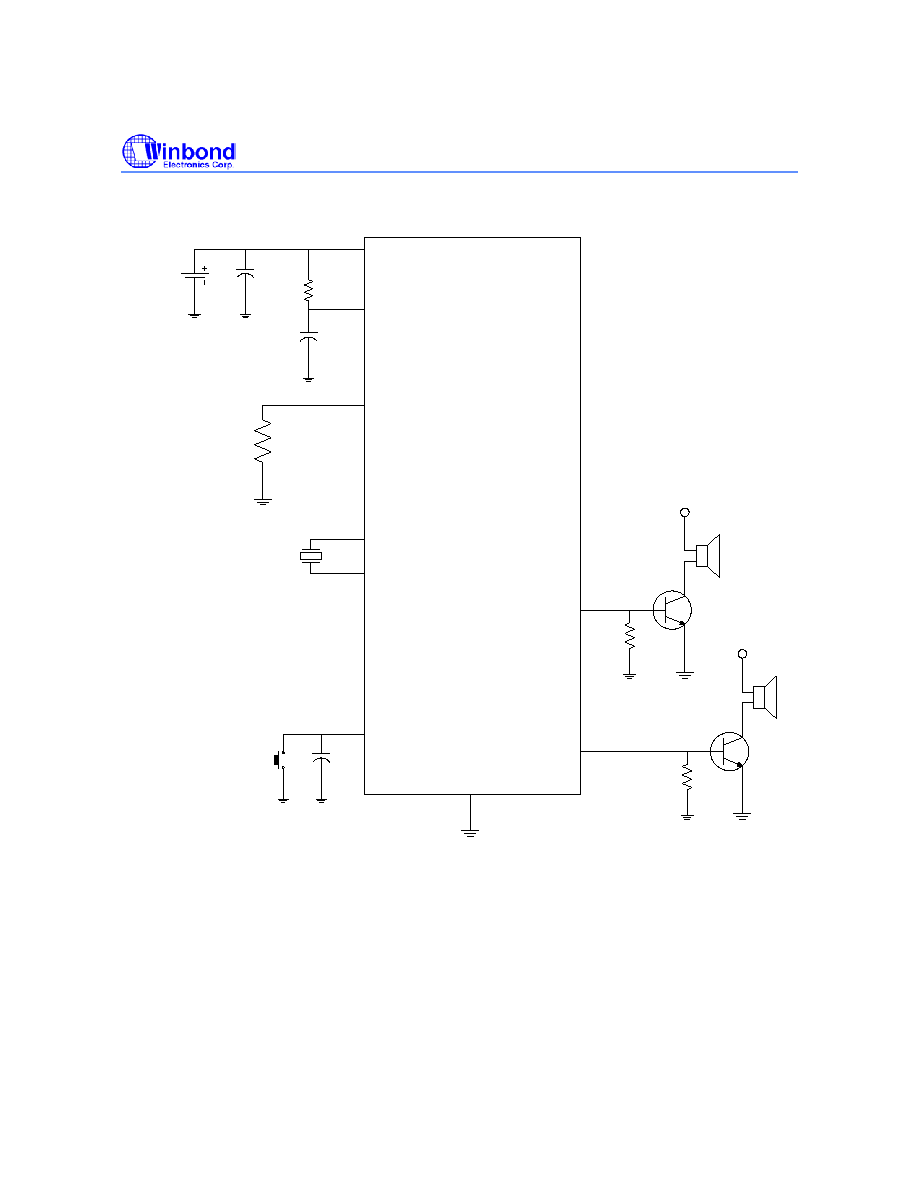
6. TYPICAL APPLICATION CIRCUIT
W567S
ROSC
OSC
X32I
X32O
VDD
VSS/
VSS1
/RESET
SPK0
SPK1
0.1uF
4.7uF
BP00
|
BP07
BP10
|
BP17
BP20
|
BP27
IP00
|
IP07
Speaker1
8050
VDD
Speaker0
8050
VDD
10
VDD1
0.1uF
32K
Notes:
1. The typical value of Rosc is 160 K
for 8 MHz and 320 K for 4 MHz and should be connected to GND (V
SS
).
2. Please refer to design guide to get typical Rosc value for each part number.
3. For W567S080~S341, V
SS
1 should be connected to V
SS
; and V
DD
1 should be connected to V
DD
in PCB layout.
4. The Rs value is suggested in 270
~ 1K to limit too large DAC output current flowing into transistor.
5. The
10
and 0.1�F between V
DD
, V
DD
1 and GND are optional to filter power noise.
6. The capacitor, 4.7
�F, shunts between V
DD
and GND is necessary as power stability. But the value of capacitor is
depend on the application.
7. The above application circuits are for reference only. No warranty for mass production.

W567SXXX
Publication Release Date: October 15, 2003
- 9 -
Revision A8
7. REVISION HISTORY
REVISION DATE
MODIFICATIONS
A1
April 2002
Preliminary release.
A2
July 11, 2002
W567S020 created.
2 speech channels for entire series.
Wording modification.
A3
July 31, 2002
Modify pin description
Modify DC/AC electrical characteristics
A4
Oct. 15, 2002
Remove SIM out of from W567S040 ~ S060
Define ROSC value in AC ELECTRICAL CHARACTERI
A5
Nov. 15, 2002
Page 2, provides up to 8 input pins
Page 2, available package
A6
May 15, 2003
Add a table to show all W567Sxxx duration in page 1
Add PowerScript
TM
function in feature list
Update available package
Rename RTC as 32 KHz crystal
Update application circuit
A7
Sep 10, 2003
Change part number W567S300 as W567S301
Change part number W567S340 as W567S341
Page 3, add Low Voltage Detect (LVD) feature
A8
Oct. 15, 2003
Update application circuit and notes.

W567SXXX
- 10 -
Headquarters
No. 4, Creation Rd. III,
Science-Based Industrial Park,
Hsinchu, Taiwan
TEL: 886-3-5770066
FAX: 886-3-5665577
http://www.winbond.com.tw/
Taipei Office
TEL: 886-2-8177-7168
FAX: 886-2-8751-3579
Winbond Electronics Corporation America
2727 North First Street, San Jose,
CA 95134, U.S.A.
TEL: 1-408-9436666
FAX: 1-408-5441798
Winbond Electronics (H.K.) Ltd.
No. 378 Kwun Tong Rd.,
Kowloon, Hong Kong
FAX: 852-27552064
Unit 9-15, 22F, Millennium City,
TEL: 852-27513100
Please note that all data and specifications are subject to change without notice.
All the trade marks of products and companies mentioned in this data sheet belong to their respective owners.
Winbond Electronics (Shanghai) Ltd.
200336 China
FAX: 86-21-62365998
27F, 2299 Yan An W. Rd. Shanghai,
TEL: 86-21-62365999
Winbond Electronics Corporation Japan
Shinyokohama Kohoku-ku,
Yokohama, 222-0033
FAX: 81-45-4781800
7F Daini-ueno BLDG, 3-7-18
TEL: 81-45-4781881
9F, No.480, Rueiguang Rd.,
Neihu District, Taipei, 114,
Taiwan, R.O.C.