
W583LXX
LOW VOLTAGE PowerSpeech
TM
Publication Release Date: May 16, 2003
- 1 -
Revision A2
Table of Contents-
1.
GENERAL DESCRIPTION ......................................................................................................... 2
2.
FEATURES ................................................................................................................................. 2
3.
BLOCK DIAGRAM ...................................................................................................................... 3
4.
PIN DESCRIPTION..................................................................................................................... 4
5.
FUNCTIONAL DESCRIPTION.................................................................................................... 6
5.1
Register Definition And Control ....................................................................................... 6
5.2
Option Control Function................................................................................................... 9
5.3
Interrupt Vector Allocation ............................................................................................... 9
5.4
Instruction Set................................................................................................................ 10
6.
ELECTRICAL CHARACTERISTICS......................................................................................... 11
6.1
Absolute Maximum Ratings........................................................................................... 11
6.2
DC Characteristics......................................................................................................... 11
6.3
AC Characteristics......................................................................................................... 12
7.
TYPICAL APPLICATION CIRCUIT........................................................................................... 12
8.
BONDING PAD DIAGRAM ....................................................................................................... 13
9.
REVISION HISTORY ................................................................................................................ 15
W583LXX
- 2 -
1. GENERAL DESCRIPTION
W583Lxxx family is a new PowerSpeech
synthesizer series with 1.8V ~ 3.6V operation voltage
range. W583Lxxx provides IR function, CPU interface, PAD option for Ring or Crystal oscillator and
voice output in DAC current or PWM type.
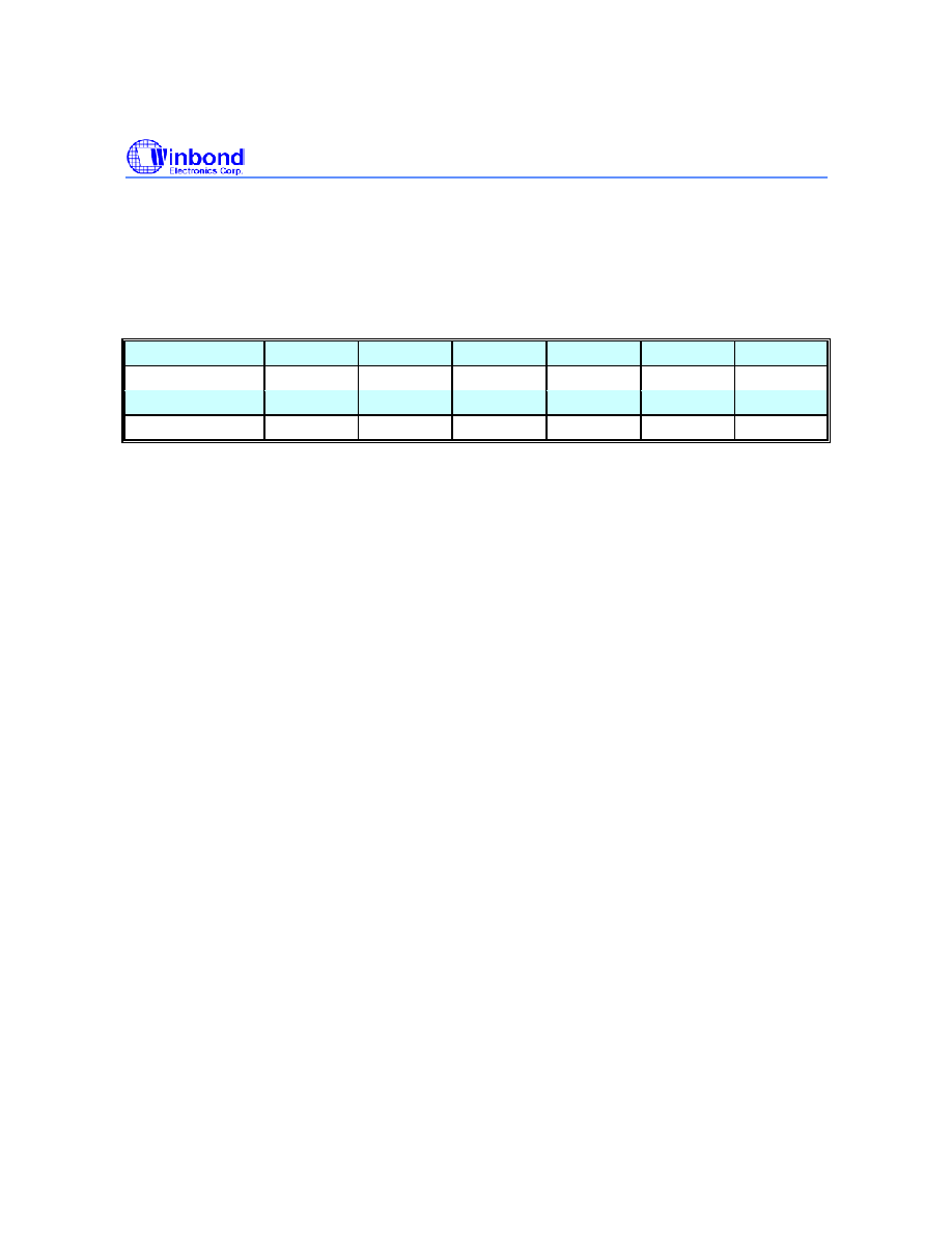
According to different voice duration, there are 8 part numbers in W583Lxxx family, listed as below.
PART NO.
W583L10
W583L15
W583L20
W583L25
W583L30
W583L40
ROM size (K bits)
384
640
768
896
1024
1472
PART NO.
W583L50
W583L60
W583L80
W583L99
W583L02
ROM size (K bits)
1760
2048
3072
3520
4096
Note: W583L10 provides less I/O pins, and do not provide crystal oscillator.
2. FEATURES
� Programmable speech synthesizer
� 5bit MDPCM algorithm to generate high sound quality
� Operating voltage range: 1.8 � 3.6 Volts
� Direct drive speaker by PWM output or Built-in 8-bit D/A converter
� Supports CPU interface operation
� IR interface for command Transmission and Receiving
� Symbolic compiler supported
� Instruction cycle 400 �S typically
� Section control
- Variable frequency: 4.8/6/8/12 KHz
- LED: ON/OFF
� Eight general-purpose registers R0-R7
� Pad option for Ring or Crystal oscillator. (W583L10 only provides Ring oscillator)
� 8 trigger inputs - with separate control of falling/rising edge trigger. (4 triggers for W583L10)
� 8 STOP outputs (5 outputs for W583L10)
� Number of interrupt vector / label up to 2,048

W583LXX
Publication Release Date: May 16, 2003
- 3 -
Revision A2
3. BLOCK DIAGRAM
TIMING
GENERATOR
CONTROLLER
SPEECH
SYNTHESIZER
D/A CONVERTER
OSC/XIN
XOUT
SEL
TG1
TG3/IRIN
TG8
STPA/BUSY
STPH
LED1
AUD/SPK+ SPK-
ROM
LED2/STPC
STPB
PWM DRIVER
VDD VSS TEST
RESET
IROUT
:
:
:
VDD1
VSS1
W583L15~L02
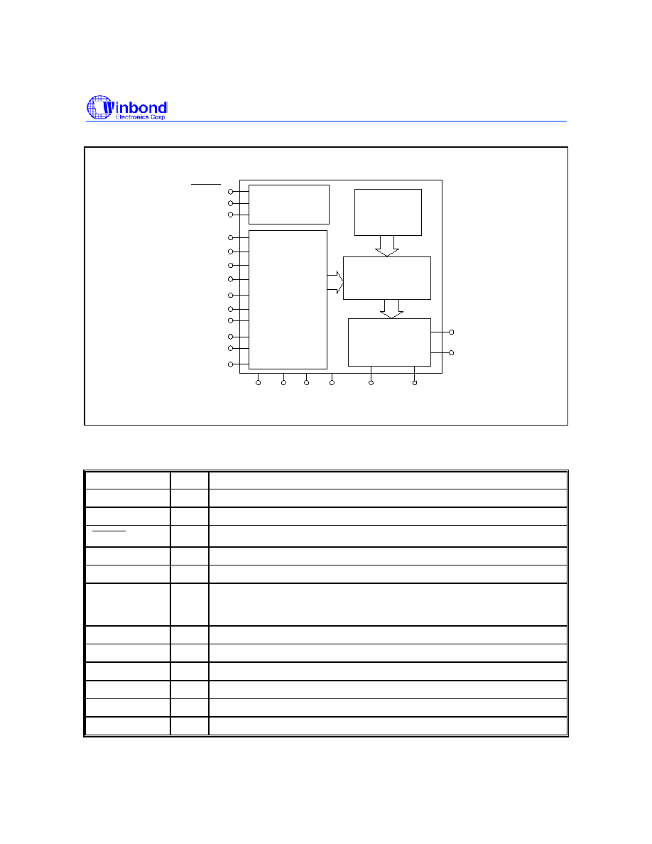
W583LXX
- 4 -
Block Diagram, continued
TIMING
GENERATOR
CONTROLLER
SPEECH
SYNTHESIZER
D/A
CONVERTER
OSC
OSCO
TG1
TG2
TG4
STPA/BUSY
STPE
LED1
AUD/SPK+
ROM
LED2/STPC
STPB
VDD VSS TEST
RESET
STPD
TG3/IRIN
SPK-
PWM DRIVER
VSS1
VDD1
IROUT
W583L10
4. PIN DESCRIPTION
NAME I/O
DESCRIPTION
V
DD
-
Positive power supply
TEST
I
Test pin, internally pulled low
RESET
I
Reset all, functions as POR, internally pulled high
TG1
I
Direct trigger input 1, internally pulled high
TG2
I
Direct trigger input 2, internally pulled high
TG3/IRIN
I
Direct trigger input 3 or IR input, internally pulled high. Once this pin is
pulled low, the oscillation circuit is active even the chip enters standby
mode.
TG4
I
Direct trigger input 4, internally pulled high
V
SS
-
Negative power supply
LED1 O
LED1
output
IROUT
O
IR signal output pin, active low
STPA/BUSY
O
Stop signal A or Busy signal
STPB
O
Stop signal B
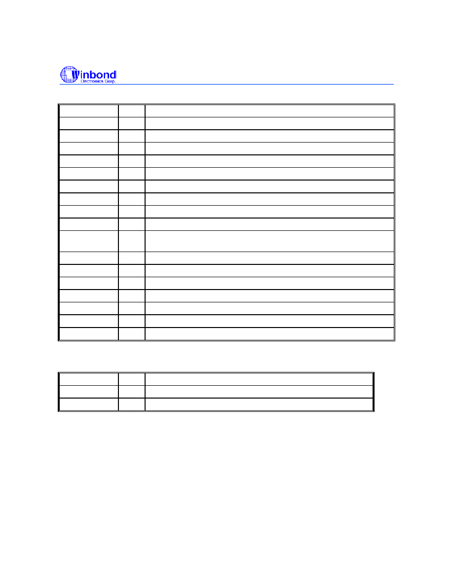
W583LXX
Publication Release Date: May 16, 2003
- 5 -
Revision A2
NAME I/O
DESCRIPTION
LED2/STPC
O
LED2 output or Stop signal C
STPD
O
Stop signal D
STPE
O
Stop signal E
AUD/SPK+
O
Current type output or PWM output for speaker
SPK- O
PWM
output
V
SS1
-
Negative power supply
V
DD1
-
Positive power supply
OSC/XIN
I
Ring oscillator input or crystal input
*XOUT
I/O
Crystal input or oscillator clock output
*SEL
I
Ring/Crystal oscillator select, internally pulled high. Floating for Ring and
grounded for crystal.
*TG5
I
Direct trigger input 5, internally pulled high
*TG6
I
Direct trigger input 6, internally pulled high
*TG7
I
Direct trigger input 7, internally pulled high
*TG8
I
Direct trigger input 8, internally pulled high
*STPF
O
Stop signal F
*STPG
O
Stop signal G
*STPH
O
Stop signal H
*: These pins no provided in W583L10
Pin Description only for W583L10
NAME I/O
DESCRIPTION
OSC
I
Ring oscillator input
OSCO
O
Oscillator clock output