Document Outline
- Main Menu
- Speech Products
- Search
- Web
Preliminary W583XXX
HIGH FIDELITY
Power Speech
TM
Publication Release Date: March 1999
- 1 -
Revision A1
GENERAL DESCRIPTION
W583xxx are fabricated using the Winbond CMOS process. The W583xxx family is a new member of
the PowerSpeech
synthesizer series, with voice quality which is even better than before. The
W583xxx family has adopted the same architecture as the PowerSpeech
synthesizers while
replacing the 4-bit ADPCM algorithm with Winbond
s new high fidelity voice synthesis algorithm to
produce better quality voice. W583xxx provides IR function, CPU interface, pad option for Ring or
Crystal oscillator and voice output in DAC current or PWM type.
According different voice duration, there are 11 bodies in W583xxx family, list them below.
PART NO.
W583S10
W583S15
W583S20
W583S25
W583S30
W583S40
Duration
10 sec
15 sec
20 sec
25 sec
30 sec
40 sec
PART NO.
W583S50
W583S60
W583S80
W583S99
W583M02
Duration
50 sec
60 sec
80 sec
99 sec
120 sec
Notes:
1. The voice duration is estimated by 6.4 KHz sampling rate.
2. W583S10 provides less I/O pins, and do not provide crystal oscillator.
FEATURES
�
Programmable speech synthesizer
�
New high fidelity synthesis algorithm
�
Wide operating voltage range: 2.4 - 5.5 Volts
�
Direct drive speaker by PWM output or Built-in 8-bit D/A converter
�
Supports CPU interface operation
�
IR interface for command Transmission and Receiving
�
Symbolic compiler supported
�
Instruction cycle
400 �S typically
�
Section control
- Variable frequency: 4.8/6/8/12 KHz
- LED: ON/OFF
�
Eight general-purpose registers R0-R7
�
Pad option for Ring or Crystal oscillator
1
�
8 trigger inputs - with separate control of falling/rising edge trigger
2
�
8 STOP outputs
3
�
Number of interrupt vector / label up to 2,048
Notes:
1. W583S10 provide ring oscillator only.
2. Only 4 trigger pins in W583S10.
3. Only 5 STOP outputs in W583S10.
Preliminary W583XXX
- 2 -
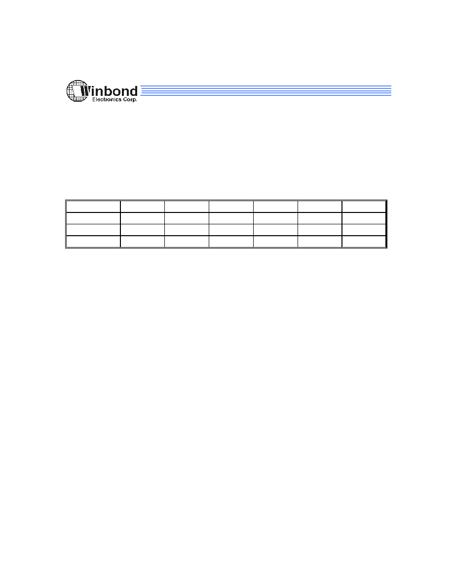
BLOCK DIAGRAM
TIMING
GENERATOR
CONTROLLER
SPEECH
SYNTHESIZER
D/A CONVERTER
OSC/XIN
XOUT
SEL
TG1
TG3/IRIN
TG8
STPA/BUSY
STPH
LED1
AUD/SPK+ SPK-
ROM
LED2/STPC
STPB
PWM DRIVER
VDD VSS TEST
RESET
IROUT
:
:
:
VDD1
VSS1
W583S15 to W583M02
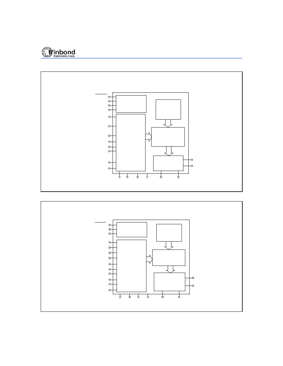
TIMING
GENERATOR
CONTROLLER
SPEECH
SYNTHESIZER
D/A
CONVERTER
OSC
OSCO
TG1
TG2
TG4
STPA/BUSY
STPE
LED1
AUD/SPK+
ROM
LED2/STPC
STPB
VDD VSS TEST
RESET
STPD
TG3/IRIN
SPK-
PWM DRIVER
VSS1
VDD1
IROUT
W583S10
Preliminary W583XXX
Publication Release Date: March 1999
- 3 -
Revision A1
PIN DESCRIPTION
NAME
I/O
DESCRIPTION
V
DD
-
Positive power supply
TEST
I
Test pin, internally pulled low
RESET
I
Reset all, functions as POR, internally pulled high
TG1
I
Direct trigger input 1, internally pulled high
TG2
I
Direct trigger input 2, internally pulled high
TG3/IRIN
I
Direct trigger input 3 or IR input, internally pulled high. Once this pin is
pulled low, the oscillation circuit is active even the chip enters standby
mode.
TG4
I
Direct trigger input 4, internally pulled high
V
SS
-
Negative power supply
LED1
O
LED1 output
IROUT
O
IR signal output pin, active low
STPA/BUSY
O
Stop signal A or Busy signal
STPB
O
Stop signal B
LED2/STPC
O
LED2 output or Stop signal C
STPD
O
Stop signal D
STPE
O
Stop signal E
AUD/SPK+
O
Current type output or PWM output for speaker
SPK-
O
PWM output
V
SS1
-
Negative power supply
V
DD1
-
Positive power supply
Pin Description only for W583S15 to W583M02
NAME
I/O
DESCRIPTION
OSC/XIN
I
Ring oscillator input or crystal input
XOUT
I/O
Crystal input or oscillator clock output
SEL
I
Ring/Crystal oscillator select, internally pulled high. Floating for Ring and
grounded for crystal.
TG5
I
Direct trigger input 5, internally pulled high
TG6
I
Direct trigger input 6, internally pulled high
TG7
I
Direct trigger input 7, internally pulled high

Preliminary W583XXX
- 4 -
Pin Description only for W583S15 to W583M02, continued
NAME
I/O
DESCRIPTION
TG8
I
Direct trigger input 8, internally pulled high
STPF
O
Stop signal F
STPG
O
Stop signal G
STPH
O
Stop signal H
Pin Description only for W583S10
NAME
I/O
DESCRIPTION
OSC
I
Ring oscillator input
OSCO
O
Oscillator clock output
FUNCTIONAL DESCRIPTION
The W583xxx is a derivative of Winbond's PowerSpeech
synthesizers, which are becoming
dominant in the consumer market, especially for toy applications.
There are up to 8 trigger inputs and 8 STOP outputs in W583xxx. The maximal number of software
key pad by scanning matrix is up to 8
� 9 = 72 keys. There are 8 general purpose registers, R0-R7.
R0-R7 can apply not only for "LD" and "JP" instructions but also for "MV" instruction. Only R0 can
apply for "INC" instruction. CPU interface is the same as the W581xx series.
IR interface is a new feature of PowerSpeech
. User can use IR interface to transmit and receive a
command. For example, when X chip executes the "TX R1" instruction, the Pulse Position Modulation
waveform (with 38 KHz carrier) outputs from IROUT pin to drive a photo diode. Y chips within a
certain distance will receive the IR signal through an IR receiver module to TG3/IRIN pin and execute
a "JP" instruction to the interrupt vector/label pointed by R1 of X chip.
There are two kinds of events that can cause the W583xxx to enter the POI (Power On Initialization)
process: one is power on, and the other is direct trigger from RESET pin. The interrupt vector "32" is
allocated for this special event, and its priority is above all, i.e., no triggers can override the POI
process if they all happen simultaneously. So the user can write a program into this interrupt vector to
set the power on initial state. If the user does not wish to execute a program on power on, he should
write an "END" instruction in interrupt vector "32". During the POI process, triggers can then override
it successfully; if the EN0, EN1 and MODE0, MODE1 registers are set properly.
If more than two events happen simultaneously, the priority that is set by the internal H/W is: POI >
TG1F > TG1R > TG2F > TG2R > TG3F > TG3R > TG4F > TG4R > TG5F > TG5R > TG6F > TG6R
> TG7F > TG7R > TG8F > TG8R > "JP" instruction.

Preliminary W583XXX
Publication Release Date: March 1999
- 5 -
Revision A1
Register Definition And Control
The register file of the W583xxx family is composed of 14 registers, including 8 general purpose
registers and 6 special purpose registers.
They are defined to facilitate the operations for various purposes. The default setting values of the
registers are given in the following table.
REGISTER
NAME
DEFAULT SETTING
General Register
R0-R7
00100000B
EN0, EN1
11111111B
Special Register
MODE0, MODE1
11111111B
STOP
11111111B
PAGE
00000000B
Note: EN1 register and bits 5-7 of STOP register are not provided in W583S10.
1. MODE0 Register
BIT
DESCRIPTION
DEFINITION
7
LED mode
1: Flash
0: DC
6
LED2/STPC
1: LED2 output
pin selection
0: STPC output
5
IR output source
1: Hardware control IR output
0: STPC control IR output
4
Debounce time
1: Long
0: Short
3, 1, 0
Reserved
-
2
STPA/BUSY
1: STPA output
pin selection
0: BUSY output
MODE0.7 controls the output type of LED1 (and LED2) pin. MODE0.6 controls the configuration of
LED2/STPC pin. MODE0.5 controls the output source of IR. If hardware control IR output is selected,
IR output can have signal with carrier or without carrier which is selected by MODE1.0. MODE0.4
controls the trigger pin debounce time. MODE0.2 controls the behavior of the STPA/BUSY pin which
is usually used as Busy signal in CPU mode.