
Publication Release Date: June 11, 2003
- 1 -
Revision 1.5
W6691
ISDN S/T Interface Transceiver
Data Sheet
The information described in this document is the exclusive intellectual property of Winbond
Electronics Corp and shall not be reproduced without permission from Winbond.
Winbond is providing this document only for reference purposes for W6691-based system design.
Winbond assumes no responsibility for errors or omissions. All data and specifications are subject to
change without notice.

W6691
- 2 -
Table of Contents-
1.
GENERAL DESCRIPTION ......................................................................................................... 8
2.
FEATURES ................................................................................................................................. 8
3.
PIN CONFIGURATIONS ............................................................................................................ 9
4.
PIN DESCRIPTION................................................................................................................... 11
5.
SYSTEM DIAGRAM AND APPLICATIONS.............................................................................. 14
6.
BLOCK DIAGRAM .................................................................................................................... 16
7.
FUNCTIONAL DESCRIPTIONS ............................................................................................... 17
7.1
Main Block Functions.................................................................................................... 17
7.1.1
Internal Block Function Description ................................................................................17
7.1.2
Interface and Operating Modes ......................................................................................18
7.2
Layer 1 Function Description........................................................................................ 18
7.2.1
S/T Interface Transmitter/Receiver.................................................................................18
7.2.2
Receiver Clock Recovery And Timing Generation..........................................................23
7.2.3
Layer 1 Activation/Deactivation ......................................................................................23
7.2.4
Layer 1 Activation /Deactivation in LT-S Mode ...............................................................29
7.2.5
D Channel Access Control..............................................................................................32
7.2.6
Frame Alignment ............................................................................................................33
7.2.7
Multiframe Synchronization ............................................................................................34
7.2.8
Test Functions................................................................................................................36
7.3
B Channel Switching..................................................................................................... 37
7.4
PCM Port ...................................................................................................................... 38
7.5
Channel HDLC Controller............................................................................................. 38
7.5.1
D Channel Message Transfer Modes .............................................................................39
7.5.2
Reception of Frames in D Channel.................................................................................40
7.5.3
Transmission of Frames in D Channel ...........................................................................41
7.6
GCI Mode Serial Interface Bus..................................................................................... 41
7.6.1
GCI Mode C/I Channel Handling ....................................................................................44
7.6.2
GCI Mode Monitor Channel Handling.............................................................................44
7.7
8-bit Microprocessor Interface ...................................................................................... 45
8.
REGISTER DESRCRIPTIONS ................................................................................................. 46
8.1
D Channel HDLC Controller Register Address Map .................................................... 46
8.2
GCI Bus Control Register Address Map....................................................................... 47
8.3
Miscellaneous Register Address Map .......................................................................... 48
8.4
D Channel HDLC Controller Register Memory Map..................................................... 49
8.5
GCI Bus Register Memory Map.................................................................................... 50
8.6
Miscellaneous Register Memory Map .......................................................................... 51

W6691
Publication Release Date: June 11, 2003
- 3 -
Revision 1.5
8.7
D Channel HDLC Controller Register Description........................................................ 51
8.7.1
D_ch receive FIFO D_RFIFO Read Address 00H .......................................................51
8.7.2
D_ch transmit FIFO D_XFIFO Write Address 01H.......................................................51
8.7.3
D_ch command register D_CMDR Write Address 02H ..................................................51
8.7.4
D_ch Mode Register D_MODE Read/Write Address 03H............................................53
8.7.5
Interrupt Status Register ISTA Read_clear Address 04H ........................................54
8.7.6
Interrupt Mask Register IMASK Read/Write Address 05H..............................................55
8.7.7
D_ch Extended Interrupt Register D_EXIR Read_clear Address 06H .........................55
8.7.8
D_ch Extended Interrupt Mask Register D_EXIM Read/Write Address 07H ...........56
8.7.9
D_ch Transmitter Status Register D_XSTA Read Address 0AH..................................56
8.7.10
D_ch Receive Status Register D_RSTA Read Address 0BH ..................................56
8.7.11
D_ch SAPI Address Mask D_SAM Read/Write Address 0EH....................................57
8.7.12
D_ch SAPI1 Register D_SAP1 Read/Write Address 0FH..........................................58
8.7.13
D_ch SAPI2 Register D_SAP2 Read/Write Address 10H ..........................................58
8.7.14
D_ch TEI Address Mask D_TAM Read/Write Address 11H .........................................58
8.7.15
D_ch TEI1 Register D_TEI1 Read/Write Address 12H ..............................................58
8.7.16
D_ch TEI2 Register D_TEI2 Read/Write Address 13H ..............................................59
8.7.17
D_ch Receive Frame Byte Count High D_RBCH Read Address 16H........................59
8.7.18
D_ch Receive Frame Byte Count Low D_RBCL Read Address 17H......................59
8.8
GCI Bus Register Description....................................................................................... 60
8.8.1
Channel Selection Register CSEL Read/Write Address 18H ................................60
8.8.2
Command/Indication Receive Register CIR Read Address 1AH .................................60
8.8.3
Command/Indication Transmit Register CIX Read/Write Address 1BH .....................60
8.8.4
S/Q Channel Receive Register SQR Read Address 1CH ..............................................61
8.8.5
S/Q Channel Transmit Register SQX Read/Write Address 1DH..................................61
8.8.6
Monitor Receive Channel 0 MO0R Read Address 20H ..........................................61
8.8.7
Monitor Transmit Channel 0 MO0X Read/Write Address 21H...................................62
8.8.8
Monitor Channel 0 Interrupt Register MO0I Read_clear Address 22H ....................62
8.8.9
Monitor Channel 0 Control Register MO0C Read/Write Address 23H.......................62
8.8.10
GCI Mode Control/Status Register GCR Read Address 26H ...............................63
8.8.11
Monitor Receive Channel 1 Register MO1R Read Address 27H ...............................63
8.8.12
Monitor Transmit Channel 1 Register MO1X Read/Write Address 28H ...........64
8.8.13
Monitor Channel 1 Interrupt Register MO1I Read_clear Address 29H ................64
8.8.14
Monitor Channel 1 Control Register MO1C Read/Write Address 2AH.......................64
8.8.15
GCI CI1 Indication Register CI1R Read Address 31H ........................................65
8.8.16
GCI CI1 Command Register CI1X Read/Write Address 32H ................................65
8.8.17
GCI Extended Interrupt Register GCI_EXIR Read_clear Address 34H ........................65
8.8.18
GCI Extended Interrupt Mask Register GCI_EXIM Read/Write Address 35H.......66

W6691
- 4 -
8.9
Miscellaneous Register................................................................................................. 66
8.9.1
Timer 1 Register TIMR1 Read/Write Address 38H ......................................................66
8.9.2
Timer 2 TIMR2 Read/ Write Address 39H ..............................................................67
8.9.3
Peripheral Control Register PCR Read/Write Address 3AH ...........................................67
8.9.4
Peripheral I/O Data Register PIODR Read/Write Address 3BH ................................68
8.9.5
SFCTL Switch Functional Control Register Read/Write Address 3CH ...........................69
8.9.6
ACTL1 Auxiliary Control Register 1 Read/Write Address 3DH.....................................70
8.9.7
ACTL2 Auxiliary Control Register2 Read/Write Address 3EH .............................70
8.9.8
ACTL3 Auxiliary Control Register 3 Read/Write Address 3FH ...................................71
8.10
B1 Channel HDLC Controller Register Address MAP.................................................. 71
8.11
B1 Channel HDLC Controller Register Memory Map................................................... 72
8.11.1
B1_ch receive FIFO B1_RFIFO Read Address 50H.............................................72
8.11.2
B1_ch transmit FIFO B1_XFIFO Write Address 51H............................................72
8.11.3
B1_ch command register B1_CMDR Read/Write Address 53H ...................................73
8.11.4
B1_ch Mode Register B1_MODE Read/Write Address 54H ......................................74
8.11.5
B1_ch Extended Interrupt Register B1_EXIR Read_clear Address 56H ......................75
8.11.6
B1_ch Extended Interrupt Mask Register B1_EXIM Read/Write Address 57H .....76
8.11.7
B1_ch Status Register B1_STAR Read Address 58H ..................................76
8.11.8
B1_ch Address Mask Register 1 B1_ADM1 Read/Write Address 59H ......................77
8.11.9
B1_ch Address Mask Register 2 B1_ADM2 Read/Write Address 5AH ........................77
8.11.10
B1_ch Address Register 1 B1_ADR1 Read/Write Address 5BH..............................78
8.11.11
B1_ch Address Register 2 B1_ADR2 Read/Write Address 5CH..............................78
8.11.12
B1_ch Receive Frame Byte Count Low B1_RBCL Read Address 5DH ...................78
8.11.13
B1_ch Receive Frame Byte Count High B1_RBCH Read Address 5EH..................78
8.11.14
B1_ch Transmit Idle Pattern B1_IDLE Read/Write Address 5FH ...............................79
8.12
B2 Channel HDLC Controller Register Address Map .................................................. 80
8.13
B2 Channel HDLC Controller Register Memory Map................................................... 81
9.
ELECTRICAL CHARACTERISTICS......................................................................................... 82
9.1
Absolute Maximum Rating............................................................................................ 82
9.2
Power Supply................................................................................................................ 82
9.3
DC Characteristics........................................................................................................ 82
9.4
Preliminary Switching Characteristics .......................................................................... 84
9.4.1
PCM Interface Timing.....................................................................................................84
9.4.2
Detailed PCM Tming ......................................................................................................85
9.4.3
8-bit Microprocessor Timing ...........................................................................................86
9.5
AC Timing Test Conditions ........................................................................................... 89
10.
ORDERING INFORMATION .................................................................................................... 89
11.
PACKAGE DIMENSIONS......................................................................................................... 90

W6691
Publication Release Date: June 11, 2003
- 5 -
Revision 1.5
List of Figures-
Fig.3.1 W6691 Pin Configuration - Intel Bus Mode................................................................................. 9
Fig.3.2 W6691 Pin Configuration � Motorola Bus Mode....................................................................... 10
Fig.5.1 ISDN Internet Passive S-card with Two POTS Connections.................................................... 14
Fig.5.2 ISDN PAXB Application............................................................................................................. 15
Fig.6.1 W6691 Functional Block Diagram............................................................................................. 16
Fig.7.1 Frame Structure at S/T Interface............................................................................................... 19
Fig.7.2 W6691 Wiring Configuration in TE Applications ....................................................................... 20
Fig.7.3 External Transmitter Circuitry.................................................................................................... 21
Fig.7.4 External Receiver Circuitry........................................................................................................ 22
Fig.7.5 Layer 1 Activation/Deaction State Diagram � TE/LT-T Normal Mode ...................................... 27
Fig.7.6 Layer 1 Activation/Deactivation State Diagram � TE/LT-T SPECIAL Mode ............................. 28
Fig.7.7 Layer 1 Activation/Deactivation State Diagram in LT-S ............................................................ 31
Fig.7.9 SSP and SCP Test Signals ....................................................................................................... 37
Fig.7.10 GCI TE Mode Channel Structure ............................................................................................ 42
Fig.7.11 GCI Non �Terminal Mode Channel Structure ......................................................................... 43

W6691
- 6 -
List of Tables-
TABLE 7.1 OUTPUT PHASE DELAY COMPENSATION TABLE ........................................................ 23
TABLE 7.2 LAYER 1 COMMAND CODES ........................................................................................... 25
TABLE 7.3 LAYER 1 INDICATION CODES ......................................................................................... 26
TABLE 7.4 LAYER 1 COMMAND CODES ........................................................................................... 29
TABLE 7.5 LAYER 1 INDICATION CODES ......................................................................................... 30
TABLE 7.8 D PRIORITY CLASSES...................................................................................................... 32
TABLE 7.9 D PRIORITY COMMANDS/INDICATIONS ........................................................................ 32
TABLE 7.10 MULTIFRAME STRUCTURE IN S/T INTERFACE .......................................................... 35
TABLE 8.1 D CHANNEL HDLC CONTROLLER REGISTER ADDRESS MAP.................................... 46
TABLE 8.2 GCI BUS CONTROL REGISTER ADDRESS MAP............................................................ 47
TABLE 8.3 MISCELLANEOUS REGISTER ADDRESS MAP .............................................................. 48
TABLE 8.4 D CHANNEL HDLC CONTROLLER REGISTER MEMORY MAP..................................... 49
TABLE 8.5 GCI BUS REGISTER MEMORY MAP................................................................................ 50
TABLE 8.6 MISCELLANEOUS REGISTER MEMORY MAP................................................................ 51
TABLE 8.7 B1 CHANNEL HDLC CONTROLLER REGISTER ADDRESS MAP.................................. 71
TABLE 8.8 B1 CHANNEL HDLC CONTROLLER REGISTER MEMORY MAP ................................... 72
TABLE 8.9 B2 CHANNEL HDLC CONTROLLER REGISTER ADDRESS MAP.................................. 80
TABLE 8.10 B2 CHANNEL HDLC CONTROLLER REGISTER MEMORY MAP................................. 81

W6691
Publication Release Date: June 11, 2003
- 7 -
Revision 1.5
REVISION HISTORY
VERSION DATE
DESCRIPTION
1.0
Jan 2001
The first version is edited.
1.1 Sep
2001
W6691 Pin Configuration -- Intel Bus mode is modified on page11.
W6691 Pin Configuration � Motorola Bus Mode is modified on page 12
Pin Description is modified on page 13.
The chapter 7.1.2 Interface and Operating Mode description is
changed on page 20.
The transformer ratio 1:1 is changed to 2:1 on Fig 7.3 and 7.4 page 23
and page 24.
1.2 Mar
2003
V
DD
and V
DDA
(output) described are error description on page 15. It is
corrected as V
DD
= 3.3V
�5%. VDDA is 5.0V output signal for chip
internal use. It should be connected with 2.2uF capacitor for supplying
stable voltage.
Add CNC and CPC pin description on page 15. The CNC pin and CPC
pin should be connected with 2.2uF for supplying stable voltage.
The Operating Supply Volatge V
DD
= 5V
�5 % in the Capacitances
description is error on page 97. It is corrected as 3.3V
�5%.
1.3 Mar
2003
The V
DD
= 5V
�5 % in chapter 9.2 power supply section should be
corrected as 3.3V
�5 %.
The V
DD
= 5V
�5 % in chapter 9.3 DC characteristic section should be
corrected as 3.3V
�5 %.
The V
DD
= 5V
�5 % in chapter 9.5 AC Timing Test Conditions should
be corrected as 3.3V
�5 %.
1.4 May
2003
The V
DDA
(output) described is error description on page 15. It is 5.0V
�5%output for monitoring. (Notice the 5.0V is generated from W6691
internal power pump)
Analog power supply current: activated section V
DD
= 5.0 V condition
described on page 100 is error. It is corrected as V
DD
= 3.3V
1.5
June 11,
2003
The XTAL2 is pin 41 described on table of page 16. It is a mistake. It is
corrected as pin39.
The pin20 decribed on page 14 is V
DD
. It is mistake. It is corrected as
WR#.
Pin37 CLKT is not described in data sheet. The description is added
on page 15.
MBIT shown page 13 and 14 is omitted. W6691 doesn't provide the
MBIT function.

W6691
- 8 -
1. GENERAL DESCRIPTION
W6691 consists of one D channel HDLC controller and two B HDLC controller channel access. The
HDLC controller facilitates efficient access to signaling, data and voice services. It provides
multiplex/non- mutiplexe 8- bit microprocessor interface. The interface is selected by external MBS
selection. In addition, W6691 can be operated in TE, LT-S and LT-T mode programmed by external
pin. In TE mode, W6691 provides PCM bus or GCI bus to connect with CODEC. In LT mode, it can
used in NT2 application. W6691 also provides various B channel switching function among PCM, GCI
and Layer2. It adopts 3.3V process to manufacture. The FIFO size of D channel is 64 byte. The FIFO
size of two B channel are 128bytes. Two extended external interrupt is designed for peripheral
interrupt saving extra interrupt circuit design. One layer activation indication output can be
programmed by microprocessor control or W6691 chip internal control. The DPLL circuit is design in
chip to generate the DCL and FSC signal for NT2 application. It can eliminate extra DPLL circuit on
board. In order to save a lot of crystal on board, W6691 can provide 7.68MHz OSC signal for other
chip needs the clock in TE or NT2 application.
2. FEATURES
� Full Duplex 2B+D S/T interface transceiver compliant with ITU I.430 Recommendation
� One D channel HDLC controller
- Maskable address recognition
- Transparent (HDLC) mode
- FIFO buffer (2 * 64)
� Two B channel HDLC controller
- Maskable address recognition
- Transparent (HDLC) mode
- FIFO buffer (2 * 128)
� Various B channel switching capabilities and PCM intercom
� Two PCM CODEC interfaces for speech and POTS application
� GCI interface connects with other peripheral device in TE, LT-S and LT-T mode.
� Multi-frame synchronization
� 8-bits Intel mode or Motorola mode interface accesses B channel and Command/Indication
channel.
� The timing clock recovery depends on operating mode.
� DPLL circuit designed in chip for NT2 application.
� Four kind of the extended interrupt trigger mode.
� Two kind of output interrupt polarity selection can be programmed. (Positive level and negative
Level)
� Added reset signal to reset other chip.
� Loop back function for testing.
� Layer1 Activate Indication Output can be connected to LED
W6691
Publication Release Date: June 11, 2003
- 9 -
Revision 1.5
� Two of programmable timer
� 3.3 Volt power supply
� 3.3 Volt output; Maximum Input is 5.0Volt
� Advanced CMOS technology
� Packaged in 64 pin LQFP
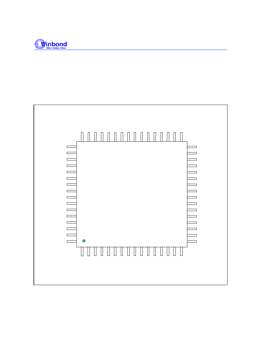
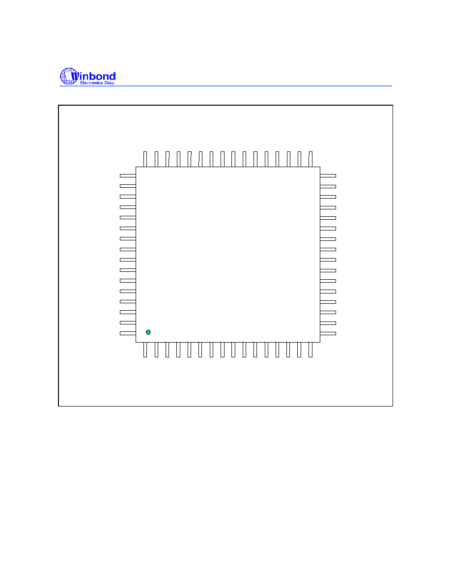
3. PIN CONFIGURATIONS
D
C
L
O
F
S
C
O
V
S
S
V
D
D
C
K
L
T
T
O
U
T
2
X
T
A
L
2
X
T
A
L
1
V
S
S
A
S
R
1
V
D
D
A
S
X
1
S
X
2
C
N
C
C
P
C
VDD
VSS
C16.384
MBS
PFCK2
PFCK1
PBCK
PTXD
PRXD
VDD
VSS
DU
DD
FSC
DCL
INT#
C
P
T
E
S
P
T
R
S
T
#
V
S
S
A
C
T
L
1
S
O
S
C
7
6
8
R
D
#
A
L
E
C
S
#
VDD
VSS
ISDN S/T Interface
Access Controller
W6691
1
2
3
4
5
6
7
8
9
10
11
12
13
14
15
16
18
17
19
20
21
22
23
24
25
26
27
28
29
30
31
32
33
34
35
36
37
38
39
40
41
42
43
44
45
46
47
48
49
50
51
52
53
54
55
56
57
58
59
60
61
62
63
64
WR#
AD7
AD6
AD5
AD4
AD3
AD2
AD1
AD0
V
D
D
S
R
2
M1
M0
Fig.3.1 W6691 Pin Configuration - Intel Bus Mode
W6691
- 10 -
Pin Confugurations, continued
D
C
L
O
F
S
C
O
V
S
S
V
D
D
C
K
L
T
T
O
U
T
2
X
T
A
L
2
X
T
A
L
1
V
S
S
A
S
R
1
V
D
D
A
S
X
1
S
X
2
C
N
C
C
P
C
VDD
VSS
C16.384
MBS
PFCK2
PFCK1
PBCK
PTXD
PRXD
VDD
VSS
DU
DD
FSC
DCL
INT#
C
P
T
E
S
P
T
R
S
T
#
V
S
S
A
C
T
L
1
S
O
S
C
7
6
8
R
W
A
L
E
C
S
#
A
7
VDD
VSS
ISDN S/T Interface
Access Controller
W6691
1
2
3
4
5
6
7
8
9
10
11
12
13
14
15
16
18
17
19
20
21
22
23
24
25
26
27
28
29
30
31
32
33
34
35
36
37
38
39
40
41
42
43
44
45
46
47
48
49
50
51
52
53
54
55
56
57
58
59
60
61
62
63
64
DS#
A
6
D7
D6
D5
D4
D3
D2
D1
D0
V
D
D
S
R
2
M1
M0
A
5
A
4
A
3
A2
A1
A0
Fig.3.2 W6691 Pin Configuration � Motorola Bus Mode

W6691
Publication Release Date: June 11, 2003
- 11 -
Revision 1.5
4. PIN DESCRIPTION
Table 4.1 W6691 pin descriptions
Note: The suffix "#" indicates an active LOW signal. In Intel or Motorola bus mode, all unspecified pins must be left
unconnected.
PIN NAME
PIN NO.
TYPE
FUNCTIONS
Intel Bus Mode (Enabled when MBS = HIGH)
MBS 52 I
Microprocessor bus selector (MBS). This pin must be
pulled to HIGH.
AD7-0
23, 24, 25, 26,
27, 28, 29, 30
I/O
Multiplexed address and data bus. During the address
phase, AD7-0 contains 8-bit physical address. During the
data phase, AD7-AD0 contains data.
CS# 11 I
Chip
select.
ALE
10
I
Address Latch Enable. Used to latch addresses.
RD# 9 I
Read.
WR# 20 I
Write.
RST# 3 I
Reset.
INT# 64 O
Interrupt. The interrupt trigger level can be programmable
by ACTL2:INTOL. It provides two types of interrupt trigger
level including low level and high level.
Motorola Bus Mode (Enabled when MBS = LOW)
MBS 52 I
Microprocessor bus selector (MBS). This pin must be
pulled to LOW.
D7-D0
23, 24, 25, 26,
27, 28, 29, 30
I/O Data
bus.
A7-A0
12, 13, 14, 15,
16, 17, 18, 19
I Address
bus.
CS# 11 I
Chip
select.
DS# 20 I
Data
strobe.
RW 9 I
Read/Write identify. HIGH is for read and LOW is for
write.
RST# 3 I
Reset.
INT# 64 O
Interrupt. The interrupt trigger level can be programmable
by ACTL2:INTOL. It provides two types of interrupt trigger
level including low level and high level.
GCI Bus
DCL
63 I/O
GCI Bus Data Clock: the frequency is twice data rate
TE mode: 1.536 MHz.
LT-T/LT-S mode: 4.096 MHz.
NT mode: 512 KHz
It needs external pull-up.

W6691
- 12 -
PIN NAME
PIN NO.
TYPE
FUNCTIONS
FSC
62 I/O
GCI Bus Frame Synchronization Clock: 8 KHz. It needs
external pull-up.
DD
61
I/O
GCI Bus Data Downstream. It needs external pull-up.
DU
60
I/O
GCI Bus Data Upstream. It needs external pull-up.
CP/BCL
1 O
CP � output 512 KHz in LT-T mode.
BCL � output 768 KHz in TE mode.
FSCO 34 O
Output FSCO clock 8 KHz for LT-T/LT-S mode (NT2
application). It is synchronous to DCLO.
DCLO 33 O
Output DPLL clock 4.096 MHz for LT-T/LT-S mode (NT2
application). It is synchronous to T interface clock.
C16.384 51 I
16.384 MHz clock input for internal DPLL circuit to generate
FSCO and DCLO.
CKLT 37 I
In the LT-T mode operation, if the application adopts
W6691 internal DPLL function to generate 8 KHz Frame
Synchronization Clock from FSCO and 4.096 MHz Data
Clock from DCLO for NT2 system clcok, the CKLT 8KHz
clock derived from one of other LT-T CP clock or itself CP
clock (by Multiplexer). On the other hand, if the application
doesn't adopts W6691 internal DPLL function, It should be
tied to ground (V
SS
).
PCM Interface (It is only used in TE Mode)
PFCK1
54 O
PCM port1 frame synchronization signal, with 8 KHz
repetition rate and 8 bits pulse width.
PFCK2
53 O
PCM port2 frame synchronization signal, with 8 KHz
repetition rate and 8 bits pulse width.
PBCK
55
O
PCM bit synchronization clock of 1.536 MHz.
PTXD 56 O
PCM transmit bus data output. A maximum of two channels
with 64 Kbits/s data rate can be multiplexed on this signal. It
needs external pull-up.
PRXD
57 I
PCM bus receive data input. A maximum of two channels
with 64 Kbits/s data rate can be multiplexed on this signal. It
needs external pull-up.
ISDN Signals and External Crystal
SR1
42
I
S/T bus receiver input (negative).
SR2
43
I
S/T bus receiver input (positive).
SX1
45
O
S/T bus transmitter output (positive).

W6691
Publication Release Date: June 11, 2003
- 13 -
Revision 1.5
PIN NAME
PIN NO.
TYPE
FUNCTIONS
SX2
46
O
S/T bus transmitter output (negative).
XTAL1 40 I
Crystal or Oscillator clock input. The clock frequency:
7.68MHz
�100PPM.
XTAL2
39
O
Crystal clock output. Left unconnected when using oscillator.
Functional Test
TESTP 2 I
Used to enable normal operation (1) or enter test mode (0).
In normal operation, it should be tied to high.
Timer2 Expiration Output
TOUT2 38 O
Timer 2 output. A square wave with 50 % duty cycle,
1~63 mS period can be generated.
Clock Pulse
OSC768 8 O
It provides output 7.68MHz clock. It does not synchronize to
S interface.
Operating Mode
M0
31
I
Setting of operating mode
M1
32
I
Setting of operating mode
Peripheral Input Port and Output Port
ACTL1S 7 O
Activate Layer1 Status.This pin can be pulled to low level or
programmed by microprocessor by ACTL2: ACTL1S when
Layer1 operates in activate.
ACTL2: ACTL1S:
0: When Layer 1 operates in activate state, ACTL1S pin is
pulled to low level. In contrast, if Layer 1 operates in
deactivate state, ACTL1S pin is driven to high level.
1: The ACTL1 output level is programmed by microprocessor
(ACTL2: ACLT1S).
Power and Ground
CNC 47
It should be connected with CPC pin 48 by 2.2uF capacitor
for stabling internal power voltage.
CPC 48
It should be connected with CNC pin 47 by 2.2uF capacitor
for stabling internal power voltage.
V
DD
5, 22, 36,
49, 58
I
Digital Power Supply (3.3V
�5%).
V
DDA
44 O
Analog Power Supply (5.0V
�5%). It should be connected
with 2.2uF capacitor for stabling internal power voltage.
V
SS
6, 21, 35,
50, 59
I Digital
Ground.
V
SSA
41 I
Analog
Ground.
W6691
- 14 -
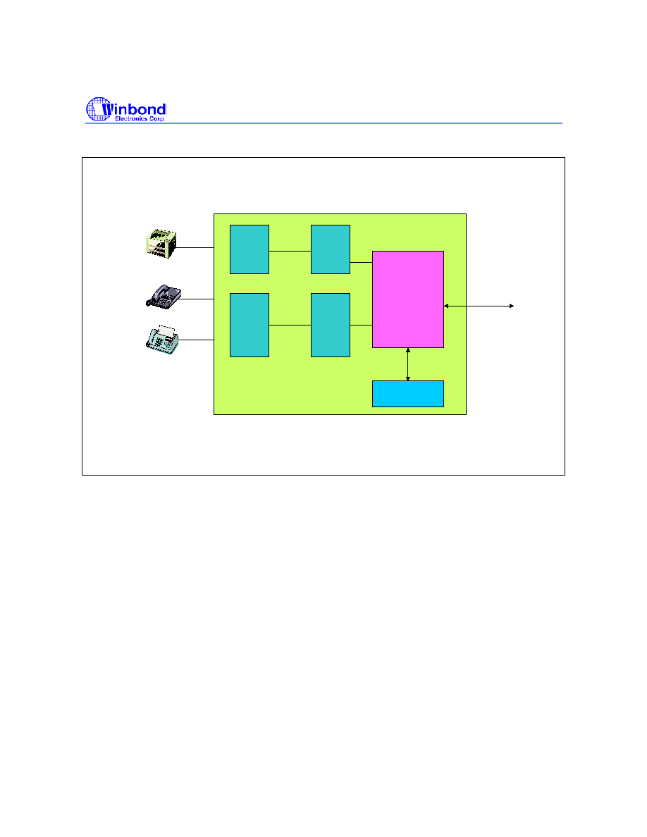
5. SYSTEM DIAGRAM AND APPLICATIONS
PCM
CODEC
X2
W6691
Transfomer
Module
POTS
Circuit
Protection
Circuit
Microprocessor
4-wire S/T
FAX
Phone
NT
S Interface
Fig.5.1 ISDN Internet Passive S-card with Two POTS Connections
W6691
Publication Release Date: June 11, 2003
- 15 -
Revision 1.5
TE
W6691
LT-S
W6691
TSI
LT-T
W6691
Clock
Generator
T interface
S interface
512KHz
4.096MHz(DCL)
8KHz(FSC)
7.68MHz
7.68MHz
GCI
GCI
UP
Fig.5.2 ISDN PAXB Application
W6691
- 16 -
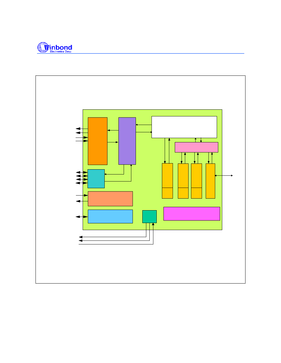
6. BLOCK DIAGRAM
The block diagram of W6691 is shown in Figure 6.1
PCM CODEC
B-channel Switching
Line
Transceiver
&
AMI/BIN
Conversion
GCI
Circuit
4-wire S/T
2B+D
2B+D
D
HDLC
Controller
FIFO
PCM
Port
Microprocessor
Interface Circuit
GCI Bus
DPLL1 and Timing Generator
Crystal/Oscillator
(7.68 MHz)
I/O Control
POTS
circuit
GCI Bus
2B+D
Slip
Buffer
B1
HDLC
Controller
FIFO
B2
HDLC
Controller
FIFO
DPLL2
FSCO
DCLO
C16.384
Fig.6.1 W6691 Functional Block Diagram

W6691
Publication Release Date: June 11, 2003
- 17 -
Revision 1.5
7. FUNCTIONAL DESCRIPTIONS
7.1 Main Block Functions
7.1.1 Internal Block Function Description
The functional block diagram of W6691 is shown in Fig.6.1. The main function blocks are:
- Layer 1 function according to ITU-T I.430
- B channel switching
- GCI bus interface
- PCM port (x 2) and internal B channel switching
- D channel HDLC controller
- DPLL 2 circiut generating 4.096 MHz clock for NT2 application
The layer 1 function includes:
- S/T bus transmitter/receiver
- Timing recovery using Digital Phase Locked Loop (DPLL) circuit
- Layer 1 activation/deactivation
- D channel access control
- Frame alignment
- Multi-frame synchronization
- Test functions
The serial interface bus performs the multiplexing/demultiplexing of D and 2B channels.
The B channel switching determines the connection between layer 1/GCI, layer 2 and PCM.
GCI bus is for TE, LT-S and LT-T mode applications.
The PCM port provides two 64 kbps clear channels to connect to PCM codec chips.
The D channel HDLC controller performs the LAPD (Link Access Procedure on the D channel)
protocol according to ITU-T I.441/Q.921 recommendation.
The peripheral simple I/O is used to control other peripheral devices such as CODEC, SLIC, DTMF
detector, LEDs.

W6691
- 18 -
7.1.2 Interface and Operating Modes
The W6691 can be configured for the following application:
ISDN terminals --- TE mode (M1 = 0 & M0 = 0)
ISDN subscriber line termination --- LT-S mode (M1=1 & M0 = 0)
ISDN trunk line termination ---LT-T mode (M1 = 0 & M0 = 1)
TE, LT-S and LT-T modes are configured by setting mode pins (M1 and M0).
7.2 Layer 1 Function Description
7.2.1 S/T Interface Transmitter/Receiver
According to ITU-T I.430, pseudo-ternary code with 100% pulse width is used in both directions of
transmission on the S/T interface. The binary "1" is represented by no line signal (zero volt), whereas
a binary "0" is represented by a positive or negative pulse.
Data transmissions on the S/T interface are arranged as frame structures. The frame is 250
�s long
and consists of 48 bits, which corresponds to a 192 kbit/s line rate. Each frame carries two octets of
B1 channel, two octets of B2 channel and four D channel bits. Therefore, the 2B+D data rate is 144
kbit/s. The frame structure is shown in Fig.7.1.
The frame begin is marked by a framing bit, which is followed by a DC balancing bit. The first binary
"0" following the framing bit balancing bit is of the same polarity as the framing bit balancing bit, and
subsequent binary zeros must alternate in polarity.

W6691
D L F L B
1
B
1
B
1
B
1
B
1
B
1
B
1
B
1
E D A F
A
N B
2
B
2
B
2
B
2
B
2
B
2
B
2
B
2
E D M B
1
B
1
B
1
B
1
B
1
B
1
B
1
B
1
E D S B
2
B
2
B
2
B
2
B
2
B
2
B
2
B
2
E D L
0
1
0
NT
TE
D L F L B
1
B
1
B
1
B
1
B
1
B
1
B
1
B
1
L D L F
A
L B
2
B
2
B
2
B
2
B
2
B
2
B
2
B
2
L D L B
1
B
1
B
1
B
1
B
1
B
1
B
1
B
1
L D L B
2
B
2
B
2
B
2
B
2
B
2
B
2
B
2
L D
0
1
0
TE
NT
48 bits in 250
�s
2 bits offset
F = Framing bit
L = DC balancing bit
N = Bit set to a binary value N=F
A
B1 = Bit within B channel 1
D = D channel bit
E = D channel echo bit
F
A
= Auxiliary framing bit or Q-bit
B2 = Bit within B channel 2
A = Bit used for activation
S = Bit used for S channel
M = Multiframe bit
Fig.7.1 Frame Structure at S/T Interface
There are three wiring configurations according to I.430: point-to-point, short passive bus and
extended passive bus. They are shown in Fig.7.2.
Publication Release Date: June 11, 2003
- 19 -
Revision 1.5

W6691
W6691
TR
TR
NT
1000 m
(a) Point-to-point configuration
TR
TR
NT
100~200 m
(b) Short passive bus configuration
W6691
TE1
TE8
. . . . .
10m
TR
TR
NT
100~200
10m
50m
TE
W6691
TE1
. . . . .
TE8
- 20 -
(c) Extended passive bus configuration
TR : Terminating Resistor
Fig.7.2 W6691 Wiring Configuration in TE Applications
The transmitter and receiver are implemented by differential circuits to increase signal to noise ratio
(SNR). The nominal differential line pulse amplitude at 100
termination is 750 mV, zero to peak.
Transformers with 2:1 turn ration are needed at transmitter and receiver for voltage level translation
and DC isolation.
To meet the electrical characteristic requirements in I.430, some additional circuits are needed. At the
transmitter side, the external resistors (5 to 10
) are used to adjust the output pulse amplitude and to
meet the transmitter active impedance (
20 ) when transmitting binary zeros. At the receiver side,
the 1.8 k
resistors protect the device inputs, while the 10 k resistors (1.8 k +8.2 k) limit the peak
current in impedance tests. The diode bridge is used for overvoltage protection.

W6691
SX1
5-10
5-10
GND
VDD
2:1
100
Publication Release Date: June 11, 2003
- 21 -
Revision 1.5
SX2
Fig.7.3 External Transmitter Circuitry
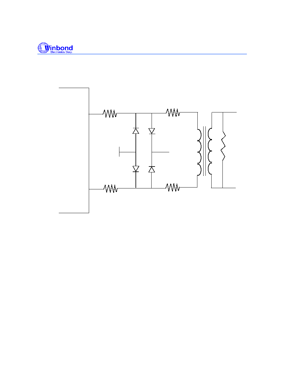
W6691
- 22 -
SR1
SR2
1.8k
1.8k
GND
VDD
8.2k
8.2k
2:1
100
Fig.7.4 External Receiver Circuitry
After hardware reset, the receiver may enter power down state in order to save power consumption. In
this state, the internal clocks are turned off, but the analog level detector is still active to detect signal
coming from the S interface. The power down state is left either by non-INFO 0 signal from S interface
or C/I command from microprocessor.

W6691
Publication Release Date: June 11, 2003
- 23 -
Revision 1.5
7.2.2 Receiver Clock Recovery And Timing Generation
1) TE mode
A Digital Phase Locked Loop (DPLL) circuit is used to derive the receiving clock from the received
data stream in TE mode application. This DPLL uses a 7.68 MHz clock as reference. According to
I.430, the transmit clock is normally delayed by 2 bit time from the receive clock. The "total phase
deviation from input to output" is -7% to +15% of a bit period. In some cases, delay compensation may
be needed to meet this requirement (see OPS1-0 bits in D_CTL register).
2) LT-T mode
In LT-T mode application, A Digital Phase Locked Loop (DPLL) circuit is also used to derive the
receiving clock(192 KHz) from the received data stream.W6691 generates a CP (Clock Pulse )
derived from the 192 KHz receiving clock with DPLL. CP clock rate is 512 KHz or 1536 KHz. If CP
clock is used to synchronize NT2 clock, W6691 provide a slip buffer to avoid slipping between DCL
and CP.
3) LT-S mode
In LT-S modes, A Digital Phase Locked Loop (DPLL) circuit is used to derive the receiving clock from
the received data stream. This DPLL uses a 7.68 MHz clock as reference.
TABLE 7.1 OUTPUT PHASE DELAY COMPENSATION TABLE
OPS1 OPS0
EFFECT
0
0
No phase delay compensation
0
1
Phase delay compensation 260 nS
1
0
Phase delay compensation 520 nS
1
1
Phase delay compensation 1040 nS
W6691 does not need RC filter on receiver side, therefore zero delay compensation is selected
normally. This is also the default setting.
The PCM output clocks (PFCK1-2, PBCK) are locked to the S-interface timing with jitter. See the
electrical specification.
7.2.3 Layer 1 Activation/Deactivation
The layer 1 activation/deactivation procedures are implemented by a finite state machine according to
TE/LT-T/LT-S mode. The state transitions are triggered by signals received at S interface or
commands issued from microprocessor. The state outputs signals to S interface and indication to
microprocessor. The CIX register is used by microprocessor to issue command, and the CIR register
is used by microprocessor to receive indication.
Some commands are used for special purposes. They are "layer 1 reset", "analog loopback", "send
continuous zeros" and "send single zero".

W6691
- 24 -
7.2.3.1 States Descriptions And Command/Indication Codes in TE/LT-T
F3 Deactivated without clock
This is the "deactivated" state of ITU-T I.430. The receive line awake unit is active except during a
hardware reset pulse. After reset, once the indication "1111" has been read out, internal clocks will
turn off and stay at this state if INFO 0 is received on the S line. The turn off time is approximate 93
ms. The ECK command must be issued to activate the clocks.
F3 Deactivated with clock
This state is identical to "F3 Deactivated without clock" except the internal clocks are enabled. The
state is entered by the ECK command. The clocks are enabled approximately 0.5 mS to 4 mS after
the ECK command, depending on the crystal capacitances. (It is about 0.5 ms for 12 pF to 33 pF
capacitance).
F3 Awaiting Deactivation
The W6691 enters this state after receiving INFO 0 (in states F5 to F8) for 16ms (64 frames). This
time constant prevents spurious effect on S interface. Any non-INFO 0 signal on the S interface
causes transition to "F5 Identifying Input" state. If this transition does not occur in a specific time (500 -
1000 ms), the microprocessor may issue DRC or ECK command to deactivate layer 1.
F4 Awaiting Signal
This state is reached when an activate request command has been received. In this state, the layer 1
transmits INFO1 and INFO 0 is received from the S interface. The software starts timer T3 of I.430
when issuing activate request command. The software deactivates layer 1 if no signal other than INFO
0 has been received on S interface before expiration of T3.
F5 Identifying Input
After the receipt of any non-INFO 0 signal from NT, the W6691 ceases to transmit INFO 1 and awaits
identification of INFO 2 or INFO 4. This state is reached at most 50
�S after a signal different from
INFO 0 is present at the receiver of the S interface.
F6 Synchronized
When W6691 receives an activation signal (INFO 2), it responds with INFO 3 and waits for normal
frames (INFO 4). This state is reached at most 6 ms after an INFO 2 arrives at the S interface (in case
the clocks were disabled in "F3 Deactivated without clock").
F7 Activated
This is the normal active state with the layer 1 protocol activated in both directions. From state "F6
Synchronized", state F7 is reached at most 0.5 ms after reception of INFO 4. From state "F3
Deactivated without clock" with the clocks disabled, state F7 is reached at most 6 ms after the W6691
is directly activated by INFO 4.
F8 Lost Framing
This is the state where the W6691 has lost frame synchronization and is awaiting resynchronization
by INFO 2 or INFO 4 or deactivation by INFO 0.

W6691
Publication Release Date: June 11, 2003
- 25 -
Revision 1.5
Special States:
Analog Loop Initiated
On Enable Analog Loop command, INFO 3 is sent by the line transmitter internally to the line receiver
(INFO 0 is sent to the line). The receiver is not yet synchronized.
Analog Loop Activated
The receiver is synchronized on INFO 3 which is looped back internally from the transmitter. The
indication 'TI" or "ATI" is sent depending on whether or not a signal different from INFO 0 is detected
on the S interface.
Send Continuous Pulses
A 96 kHz continuous pulse with alternating polarities is sent.
Send Single Pulses
A 2 KHz , isolated pulse with alternating polarities is sent.
Layer 1 Reset
A layer 1 reset command forces the transmission of INFO 0 and disables the S line awake detector.
Thus activation from NT is not possible. There is no indication in reset state. The reset state can be
left only with ECK command.
TABLE 7.2 LAYER 1 COMMAND CODES
COMMAND SYM.
CODE
DESCRIPTION
Enable clock
ECK
0000 Enable internal clocks
Layer 1 reset
RST
0001 Layer 1 reset
Send continuous pulses
SCP
0100 Send continuous pulses at 96 KHz
Send single pulses
SSP
0010 Send isolated pulses at 2 KHz
Activate request at priority 8
AR8
1000
Activate layer 1 and set D channel priority level to
8
Activate request at priority 10 AR10
1001 Activate layer 1 and set D channel priority to 10
Enable analog loopback
EAL
1010 Enable analog loopback
Deactivate layer 1
DRC
1111 Deactivate layer 1 and disable internal clocks

W6691
- 26 -
TABLE 7.3 LAYER 1 INDICATION CODES
INDICATION SYM.
CODE
DESCRIPTIONS
Clock Enabled
CE
0111 Internal clocks are enabled
Deactivate request
downstream
DRD 0000
Deactivation request by S interface, i.e INFO 0
received
Level detected
LD
0100 Signal received, receiver not synchronous
Activate request downstream ARD
1000 INFO 2 received
Test indication
TI
1010
Analog loopback activated or continuous zeros or
single zeros transmitted
Awake test indication
ATI
1011 Level detected during test function
Activate indication with
priority class 1
AI8
1100 INFO 4 received, D channel priority is 8 or 9
Activate indication with
priority class 2
AI10
1101 INFO 4 received, D channel priority is 10 or 11
Clock disabled
CD
1111 Layer 1 deactivated, internal clocks are disabled
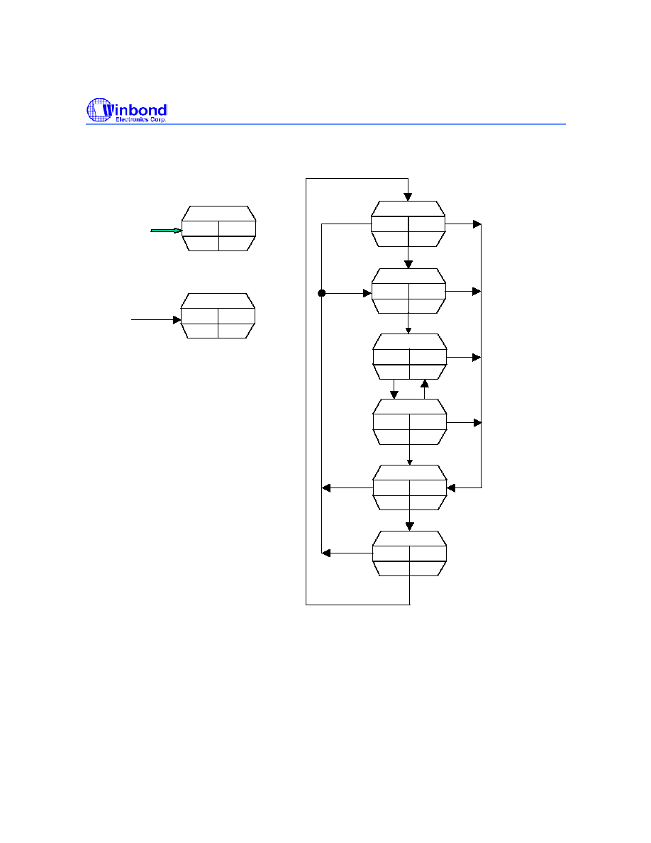
7.2.3.2 State Transition Diagrams in TE/LT-T
The followings are the state transition diagrams, which implement the activation/deactivation state
matrix in I.430 (TABLE 5/I.430). The "command" and "s receive" entries in each state octagon keep
the state, the "indication" and "s transmit" entries in each state octagon are the state outputs. For
example, at "F3 Deactivated with clock" state, the layer 1 will stay at this state if the command is
"ECK" and the INFO 0 is received on S interface. At this state, it provides "CE" indication to the
microprocessor and transmits INFO 0 on S interface. The "AR8/10" command causes transition to F4
and non-INFO 0 signal causes transition to F5. Note that the command code writtern by the
microprocessor in CIX register and indication code written by layer 1 in CIR register are transmitted
repeatedly until a new code is written.
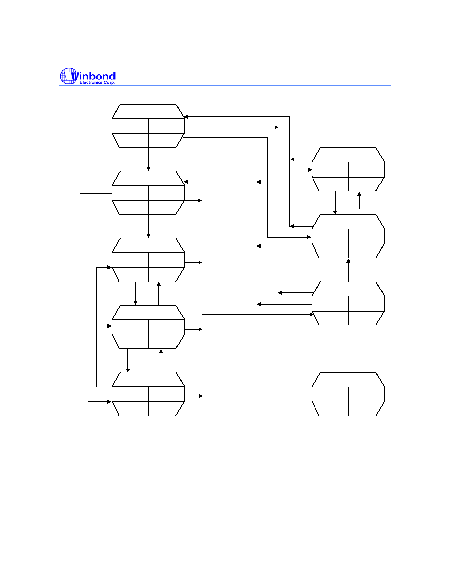
W6691
State
com
Ind
s receive
s trans.
F4 Await. Signal
AR8/10
CE
i0
i1
F5 Ident. Input
^RST
1)
LD
any
2)
i0
F6 Synchronized
^RST
1)
ARD
i2
i3
F7 Activated
AR8/10
AI8/10
i4
i3
F8 Lost Framing
^RST
1)
LD
any
2)
i0
F3 Deact w/o clk
DRC
CD
i0
i0
F3 Deact with clk
ECK
CE
i0
i0
F3 Await. Deact.
AR8/10
DRD
i0
i0
Notation:
AR8/10
AR8/10
DRC
ECK
DRC
DRC
ECK
ECK
^i0
3)
^i0
3)
^i0
3)
^i0
3)
i0
i0
i0
i0
i2
i4
i2
i4
Lost
Framing
i4
i2
Lost
Framing
Publication Release Date: June 11, 2003
- 27 -
Revision 1.5
Notes:
1. "^RST" means "NOT layer 1 reset command".
2. "Any" means any signal other than i0, which has not yet been determined.
3. "^i0" means any signal other than i0 Fig.7.5 layer 1 activation/deactivation state diagram - normal mode
Fig.7.5 Layer 1 Activation/Deaction State Diagram � TE/LT-T Normal Mode
W6691
- 28 -
State
com
Ind
s receive
s trans.
Reset
RST
None
Ignored
i0
Send Cont. Pulses
SCP
TI
Ignored
ic
3)
Send Sing. Pulses
SSP
TI
Ignored
is
4)
Ana. Loop Init.
EAL
CE
Ignored
i3
5)
Ana. Loop Act.
EAL
TI/ATI
Ignored
i3
5)
RST
SCP
SSP
EAL
ECK
Y
2)
Y
2)
Y
2)
Y
2)
i3
5)
^i3
5)
Notation:
Notes:
1. RST can be issued at any state, while SCP, SCZ and EAL can be issued only at F3 or F7.
Fig.7.6 Layer 1 Activation/Deactivation State Diagram � TE/LT-T SPECIAL Mode
2. Y is one of the commands: ECK, DRC, RST.
3. Continuous pulses at 96 KHz.
4. Isolated pulses at 2 KHz.
5. The INFO 3 is transmitted internally only.

W6691
Publication Release Date: June 11, 2003
- 29 -
Revision 1.5
7.2.4 Layer 1 Activation /Deactivation in LT-S Mode
7.2.4.1 States Descriptions and Command/Indication Codes in LT-S Mode
G1 Deactivated
No any signal is detected on S interface and No any activation command is received in the C/I
channel.
G2 Pending Activation
If INFO1 is detected on S interface or an ARD command is received from layer2, the W6691 start to
transmit INFO2. W6691 is waiting for receiving INFO3 from S interface. INFO2 is sent from W6691.
G3 Activated
W6691 receives INFO3, then, it enters G3 activated state. The INFO4 is transmitted in this state.
When the synchronization is lost, W6691 switch to transmit INFO2 instead of INFO4 and wait for
receiving INFO3 to get synchronization again.
G4 Pending Deactivation
This state is requested by DDR (deactivate request). If INFO0 is received during 16ms or an internal
timer2 expiration, the layer1 responses DRIU indication for
Layer2.
G4 Await Deactivated
The W6691 stays in this state and waits for DRIU report from layer2. If W6691 receives DRA
command from layer2, it enters G1 state.
Test Mode Continuous Pulses
Continuous alternating 96 KHz pulses are sent.
Test Mode Single Pulses
Single alternating 2 KHz pulses are sent.
TABLE 7.4 LAYER 1 COMMAND CODES
COMMAND SYM.
CODE
DESCRIPTION
Deactivate down request
DDR
0000 Deactive Layer1 and disable internal clocks
Send continuous pulses
SCP
0011 Send continuous pulses at 96 KHz
Send single pulses
SSP
0010 Send isolated pulses at 2 KHz
Activate request
downstream
ARD
1000 Request Layer1 activate Info2/Info4 sent
Deactivate request assure
DRA
1111
Layer2 reponses Deactivate acknowledgement to
make sure Layer1 can be deativate
RESET
RST
0001 Initialize to G4 or G1 state

W6691
- 30 -
TABLE 7.5 LAYER 1 INDICATION CODES
INDICATION SYM.
CODE
DESCRIPTIONS
Signal Synchronize
SSYU
0100
Received signal is not Info3 and try to re-synchronize
again
Activate Request
Indication Upstream
ARIU
1000
The INFO 1 signal detected is responsed to Layer2.
Activate Indication
upstream
AIU 1100
Synchronous
receiver
Deactivate Request
Indication Upstream
DRIU 1111
Timer2 expired
Info 0 received during 25ms after deactivation request
command
RESET Indication
RSTI
0001
Reset state indication
Test Indication
TI
0000
W6691
IS: continuous 96 KHz pulse signal or single 2 KHz pulse
signal
ARD or i1
G1 Deact
DDR
DRIU
i0
i0
G2 Pending Act
DDR/ARD
ARIU
I0/i1
i2
i3
G3 Activated
DDR/ARD
AIU
^i3
i4
DDR/ARD
SSYN
i2
G4 pending deact
DDR
i0
i0/i1/i3
DDR
AIU
G4 Await deact
DDR
DDR
Reset
REST
RES
i0
i0/i1/i3
Test Mode
TI
SCP/SSP
IS
i0/i1/i3
SCP/SSP
RST
DDR
i3
i3
Lost of Frame
i0 during 25ms or T2 expire
ARD
ARD
DDR
^i3
7.2.4.2 States Transition Diagram in LT-S Mode
ARD
Publication Release Date: June 11, 2003
- 31 -
Revision 1.5
DDR
DRIU
i0
i0/i3
DRA
Fig.7.7 Layer 1 Activation/Deactivation State Diagram in LT-S

W6691
- 32 -
7.2.5 D Channel Access Control
The D channel access control includes collision detection and priority management. The collision
detection is always enabled. The priority management procedure as specified in ITU-T I.430 is fully
implemented in W6691.
A collision is detected if the transmitted D bit and the received echo bit do not match. When this
occurs, D channel transmission is immediately stopped, and the echo channel is monitored to attempt
the next D channel access.
There are two priority classes: class 1 and class 2. Within each class, there are normal and lower
priority levels.
TABLE 7.8 D PRIORITY CLASSES
NORMAL
LEVEL
LOWER
LEVEL
Priority class 1
8
9
Priority class 2
10
11
The selection of priority class is via the AR8/AR10 command. The following table summarizes the
commands/indications used for setting the priority classes:
TABLE 7.9 D PRIORITY COMMANDS/INDICATIONS
COMMAND SYM.
CODE
REMARKS
Activate request, set priority 8
AR8
1000 Activation command, set D channel priority to 8
Activate request, set priority 10
AR10
1001
Activation command, set D channel priority to
10
Indication Abbr.
Remarks
Activate indication with priority 8
AI8
1100 Info 4 received, D channel priority is 8 or 9
Activate indication with priority 10
AI10
1101 Info 4 received, D channel priority is 10 or 11

W6691
Publication Release Date: June 11, 2003
- 33 -
Revision 1.5
7.2.6 Frame
Alignment
The following sections describe the behavior of W6691 in respect to the CTS-2 conformance test
procedures for frame alignment. Please refer to ETSI-TM3 Appendix B1 for detailed descriptions.
7.2.6.1 FAinfA_1fr
This test checks if TE does not lose frame alignment on receipt of one bad frame. The pattern for the
bad frame is defined as IX_96 KHz. This pattern consists of alternating pulses at 96 KHz during the
whole frame.
Device Settings Result
W6691 None Pass
7.2.6.2 FAinfB_1fr
This test checks if TE does not lose frame alignment on receipt of one IX_I4noflag frame which has no
framing and balancing bit.
Device Settings Result
W6691 None Pass
7.2.6.3 FAinfD_1fr
This test checks if TE does not lose frame alignment on receipt of one IX-I4viol16 frame. The
IX_I4viol16 frame remains at binary "1" until the first B2 bit which is bit position 16. The pulse
sequences are: Framing bit, balancing bit, B2 bit, M bit, S bit, balancing bit. The TE should reflect the
received F
A
bit (F
A
="1") in the transmitted frame.
Device Settings Result
W6691 None Pass
7.2.6.4 FAinfA_kfr
This is to test the number k of IX_96 KHz frames necessary for loss of frame alignment.
Device Settings Result
W6691
k = 2
Pass
7.2.6.5 FAinfB_kfr
This is to test the number k of IX_I4noflag frames necessary for loss of frame alignment.
Device Settings Result
W6691
k = 2
Pass

W6691
- 34 -
7.2.6.6 FAinfD_kfr
This is to test the number k of IX_I4noflag frames necessary for loss of frame alignment.
Device Settings Result
W6691
k = 2
Pass
7.2.6.7 Faregain
This is to test the number m of good frames necessary for regain of frame alignment. The TE regains
frame alignment at m+1 frame.
The W6691 achieves synchronization after 5 frames, i.e m = 4.
Device Settings Result
W6691
m = 4
Pass
7.2.7 Multiframe
Synchronization
As specified by ITU-T I.430, the Q bit is transmitted from TE to NT in the position normally occupied
by the auxiliary framing bit (F
A
) in one frame out of 5, whereas the S bit is transmitted from NT to TE.
The S and Q bit positions and multiframe structure are shown in Table 7.10.
The functions provided by W6691 are:
- Multiframe synchronization: Synchronization is achived when the M bit pattern has been correctly
received during 20 consecutive frames starting from frame number 1.
Note: Criterion for multiframe synchronization is not defined in I.430 Recommendation.
- S bits receive and detect: When synchronization is achieved, the four received S bits in frames
1,6,11,16 are stored as S1 to S4 in the SQR register respectively. A change in the recived four bits
(S1-4) is indicated by an interrupt.
- Multiframe synchronization monitoring: Multiframe synchronization is constantly monitored. The
synchronization state is indicated by the MSYN bit in the SQR register.
- Q bits transmit and F
A
mirroring: When multiframe synchronization is achived, the four bits Q1-4
stored in the SQXR register are transmitted as the four Q bits (F
A
-bit position) in frames 1,6,11 and
16. Otherwise the F
A
bit transmitted is a mirror of the received F
A
-bit. At loss of synchronization,
the mirroring is resumed at the next F
A
-bit.
- The multiframe synchronization can be disabled by setting MFD bit in the D_MODE register.
- According to I.430 Recommendation, the S/Q channel can be used as operation and maintenance
signalling channel. At transmitter, a S/Q code for a message shall be repeated at least six times or
as many as necessary to obtain the desired response. At receiver, a message shall be considered
received only when the proper codes is received three consecutive times.

W6691
Publication Release Date: June 11, 2003
- 35 -
Revision 1.5
TABLE 7.10 MULTIFRAME STRUCTURE IN S/T INTERFACE
FRAME
NUMBER
NT-to-TE
F
A
-bit position
NT-to-TE
M bit
NT-to-TE
S bit
TE-to-NT
F
A
-bit position
1
2
3
4
5
ONE
ZERO
ZERO
ZERO
ZERO
ONE
ZERO
ZERO
ZERO
ZERO
S1
ZERO
ZERO
ZERO
ZERO
Q1
ZERO
ZERO
ZERO
ZERO
6
7
8
9
10
ONE
ZERO
ZERO
ZERO
ZERO
ZERO
ZERO
ZERO
ZERO
ZERO
S2
ZERO
ZERO
ZERO
ZERO
Q2
ZERO
ZERO
ZERO
ZERO
11
12
13
14
15
ONE
ZERO
ZERO
ZERO
ZERO
ZERO
ZERO
ZERO
ZERO
ZERO
S3
ZERO
ZERO
ZERO
ZERO
Q3
ZERO
ZERO
ZERO
ZERO
16
17
18
19
20
ONE
ZERO
ZERO
ZERO
ZERO
ZERO
ZERO
ZERO
ZERO
ZERO
S4
ZERO
ZERO
ZERO
ZERO
Q4
ZERO
ZERO
ZERO
ZERO
1
2
etc.
ONE
ZERO
ONE
ZERO
S1
ZERO
Q1
ZERO

W6691
- 36 -
7.2.8 Test
Functions
The W6691 provides loop and test functions as follows:
- Digital loop via DLP bit in D_MODE register: In the layer 2 block, the transmitted 2B+D data are
internally looped (from HDLC transmitter to HDLC receiver), and in the PCM ports, the
transmitted B channels are internally looped (from PCM inputs to PCM outputs). The clock
timings are generated internally and are independent of the S bus timing. This loop function is
used for test of PCM and higher layer functions, excluding layer 1. After hardware reset,
W6691 will power down if S bus is not connected or if there is no signal on the S bus. In this
case, the C/I command ECK must be issued to power up the chip.
- Analog loop via the C/I command EAL: The analog S interface transmitter is internally
connected to the S interface receiver. When the receiver has synchronized itself to the internal
INFO 3 signal, the message "Test Indication" or "Awake Test Indication" is delivered to the CIR
register. No signal is transmitted over the S interface.
In this mode, the S interface awake detector is enabled. Therefore if a level (INFO 2/ INFO 4) is
detected on the S interface, this will be reported by the "Awake Test Indication (ATI)" indication.
- Remote loopback via RLP bit in D_MODE register: The digital 2B data received from the S
interface receiver is loopbacked to the S interface transmitter. The D channel is not looped.
When RLP is enabled, layer 1 D channel is connected to HDLC port and DLP cannot be
enabled.
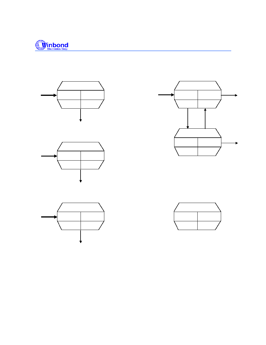
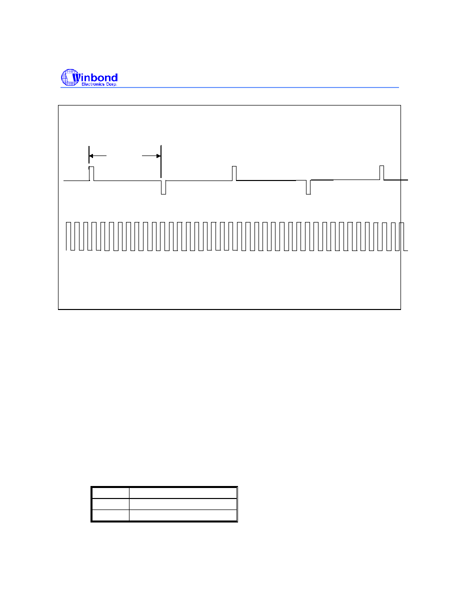
- Transmission of special test signals via layer 1 command:
* Send Single Pulses (SSP): To send isolated single pulses of alternating polarity, with pulse
width of one bit time, 250
�S apart, with a repetition frequency of 2 KHz.
* Send Continuous Pulses (SCP): To send continuous pulses of alternating polarity, with pulse
width of bit time. The repetition frequency is 96 KHz.
W6691
Publication Release Date: June 11, 2003
- 37 -
Revision 1.5
250 us
(a) Single pulses
(b) Continuous pulses
Fig.7.9 SSP and SCP Test Signals
7.3 B Channel Switching
W6691 provides five kinds of B channel switching function.
1. PCM and GCI bus Switch (SFCTL: PGSWH):
It determines the CODEC interface is to be operated in B channel.
1: PCM bus is selected to operate with CODEC.
0: GCI bus is selected to operate with CODEC.
2. PCM Remote Loop Back (SFCTL: PCRLP)
Setting this bit activates the PCM channel remote loopback function. The transmitted PCM data to
PCM channel are looped to received PCM channel.
3. PXC PCM Cross-connect (SCFT: PXC)
This bit determines whether or not the PCM ports are cross-connected with the B channel ports. The
setting of PXC is independent of the BSW1-0 bits.
PXC Connection
0
PCM1
B1, PCM2 B2
1
PCM1
B2, PCM2 B1

W6691
- 38 -
4. B2SW1 / B2SW0 B2 channel Switch
These two bits determine B2 channel switch among PCM port, Layer1/GCI and Layer2.
00: Select B2 channel switch between Layer2 and Layer1/GCI.
01: Select B2 channel switch between Layer1/GCI and PCM.
10: Select B2 channel switch between PCM and Layer2.
5. B1SW1 / B1SW0 B1 channel Switch
These two bits determine B1 channel switch among PCM port, Layer1/GCI and Layer2.
00: Select B1 channel switch between Layer2 and Layer1/GCI.
01: Select B1 channel switch between Layer1/GCI and PCM.
10: Select B1 channel switch between PCM and Layer2.
7.4 PCM Port
There are two PCM ports in W6691. Data is valid when respective PFCK is HIGH. The frame
synchronization clocks (PFCK1-2) are 8 KHz and the bit synchronization clock (PBCK) is 1.536 MHz.
7.5 Channel HDLC Controller
There are two HDLC protocols that are used for ISDN layer 2 functions: LAPD and LAPB. Their frame
formats are shown below.
LAPB modulo 8:
flag
(1 octet)
address
(1octet)
control
(1octet)
information
(0 or N octets)
FCS
(2 octets)
flag
(1 octet)
Control
field
bits 7 6 5 4 3 2 1 0
I frame
N(R)
P
N(S)
0
S frame
N(R)
P/F
S
S
0
1
U
frame
M M M P/F M M 1 1
W6691
Publication Release Date: June 11, 2003
- 39 -
Revision 1.5
LAPB modulo 128:
flag
(1 octet)
address
(1octet)
control
(1 or 2
octets)
information
(0 or N octets)
FCS
(2 octets)
flag
(1 octet)
1st
octet
2nd
octet
Control
field
bits 7 6 5 4 3 2 1 0 7 6 5 4 3 2 1 0
I frame
N(S)
0
N(R)
P
S
frame
X X X X S S 0 1 N(R) P/F
U
frame
M
M
M
P/F
M
M
1 1
LAPD : modulo 128 only
flag
(1 octet)
address
(2 octets)
control
(2 octets)
information
(0 or N octets)
FCS
(2 octets)
flag
(1 octet)
1st
octet
2nd
octet
Control
field
bits 7 6 5 4 3 2 1 0 7 6 5 4 3 2 1 0
I frame
N(S)
0
N(R)
P/F
S
frame
0 0 0 0 S S 0 1 N(R) P/F
U
frame
M
M
M
P/F
M
M
1 1
7.5.1 D Channel Message Transfer Modes
The D channel HDLC controller operates in transparent mode.
Chracteristics:
- Receive frame address recognition
- Address comparison maskable bit-by-bit
- Flag generation / deletion
- Zero bit insertion/ deletion
- Frame Check Sequence (FCS) generation/ check with CRC_ITU-T
Note. The LAPD protocol uses the CRC_ITU-T for Frame Check Sequence. The polynominal is X
16
+ X
12
+ X
5
+ 1.

W6691
- 40 -
For address recognition, the W6691 provides four programmable registers for individual SAPI and TEI
values, SAP1-2 and TEI1-2, plus two fixed values for group SAPI and TEI, SAPG and TEIG. The
SAPG equals 02H(C/R = 1) or 00H(C/R = 0) which corresponds to SAPI = 0. The TEIG equals FFH
which corresponds to TEI = 127. Incoming frame with 1
st
address octet = (SAP1 or SAP2 or SAPG)
and 2
nd
address octet = (TEI1 or TEI2 or TEIG) will be stored in the receive FIFO, with flag and FCS
fields being discarded and stuffed bits being removed.
The valid address combinations are:
- SAP1 and TEI1
- SAP1 and TEI = 127
- SAP2 and TEI2
- SAP2 and TEI = 127
- SAPI = 0 and TEI1
- SAPI = 0 and TEI2
- SAPI = 0 and TEI = 127
The receive frame address comparisons can be disabled (masked) per bit basis by setting the
D_SAM and D_TAM registers, but comparisons with the SAPG or TEIG cannot be disabled.
7.5.2 Reception of Frames in D Channel
A 128-byte FIFO is provided in the receive direction. The data movement is handled by interrupts.
There are two interrupt sources: Receive Message Ready (D_RMR) and Receive Message End
(D_RME). The D_RMR interrupt indicates that at least 64 bytes of data have been received and the
message/ frame is not ended. Upon D_RMR interrupt, the microprocessor reads out 32 bytes of data
from the FIFO. The D_RME interrupt indicates the last segment of a message or a message with
length
32 bytes has been received. The length of data is less than or equal to 32 and is specified in
the D_RBCL register.
If the length of the last segment of message is 32, only D_RME interrupt is generated and the RBC4-0
bits in D_RBCL register are 000000B.
The data between the opening flag and the CRC field are stored in D_RFIFO. For LAPD frame, this
includes the address field, control field and information field.
When a D_RMR or D_RME interrupt is generated, the micro-processor must read out the data from
D_RFIFO and issues the Receive Message Acknowledgement command (D_CMDR: RACK bit) to
explicitly acknowledge the interrupt. The microprocessor must handle the interrupt before more than
32 bytes of data are received. This corresponds to a maximum microprocessor reaction time of 16 ms
at 16 kbps data rate.
If the microprocessor is late in handling the interrupt, the incoming additional bytes will result in a
"data overflow" interrupt and status bit.

W6691
Publication Release Date: June 11, 2003
- 41 -
Revision 1.5
7.5.3 Transmission of Frames in D Channel
A 64-byte FIFO is provided in the transmit direction. If the transmit FIFO is ready (which is indicated
by a D_XFR interrupt), the micro-processor can write up to 32 bytes of data into the FIFO and use the
XMS command bit to start frame transmission. The HDLC transmitter sends the opening flag first and
then sends the data in the transmit FIFO.
The microprocessor must write the address, control and information field of a frame into the transmit
FIFO.
Every time no more than 32 bytes of data are left in the transmit FIFO, the transmitter generates a
D_XFR interrupt to request another block of data. The microprocessor can then write further data to
the transmit FIFO and enables the subsequent transmission by issuing an XMS command.
If the data written to the FIFO is the last segment of a frame, the microprocessor issues the XME
(Transmit Message End) and XMS command bits to finish the frame transmission. The transmitter
then transmits the data in the FIFO and appends CRC and closing flag.
If the microprocessor fails to respond the D_XFR interrupt within a given time (16 ms), a data
underrun condition will occur. The W6691 will automatically reset the transmitter and send inter frame
time fill pattern (all 1's) on D channel. The microprocessor is informed about this condition via an
XDUN (Transmit Data Underrun) interrupt in D_EXIR register. The microprocessor must wait until
transmit FIFO ready (via XFR interrupt), re-write data, and issue XMS command to re-transmit the
data.
It is possible to abort a frame by issuing a D_CMDR: XRST (D channel Transmitter Reset) command.
The XRST command resets the transmitter and causes a transmit FIFO ready condition.
After the microprocessor has issued the XME command, the successful termination of transmission is
indicated by an D_XFR interrupt.
The inter-frame time fill pattern must be all 1's, according to ITU-T I.430.
Collisions which occur on the D channel of S interface will cause an D_EXIR: XCOL interrupt. A XRST
(Transmitter Reset) command must be issued and software must wait until transmit FIFO ready (via
XFR interrupt), re-write data, and issue XMS command to re-transmit the data.
7.6 GCI Mode Serial Interface Bus
The GCI is a generalization and enhancement of the general purpose, serial interface bus. The
channel structure of the GCI mode is depicted below. The timing is compatible with Siemens's IOM-2
mode.
W6691
- 42 -
TE Mode Timing
TE mode contains three channels. The structure of TE mode is show in Fig7.10.
DU
/
DD
B1
B2
M0
D CI0
CI1
M1
AE
E
A
CH0
CH1
CH2
FSC
125us
B1 : 64 Kbits/s B channel 1
B2 : 64 Kbits/s B channel 2
M0 : Monitor channel 0
D : 16Kbits/s D channel
CI0: 48Kbits/s Command / Indication Channel
A/E : 16Kbits Monitor channel handshake signaling
M1: Monitor channel1
CI1: 48Kbits/s Command / Indication Channel
FSC
DCL
Fig.7.10 GCI TE Mode Channel Structure
W6691
Publication Release Date: June 11, 2003
- 43 -
Revision 1.5
Non-TE mode Timing
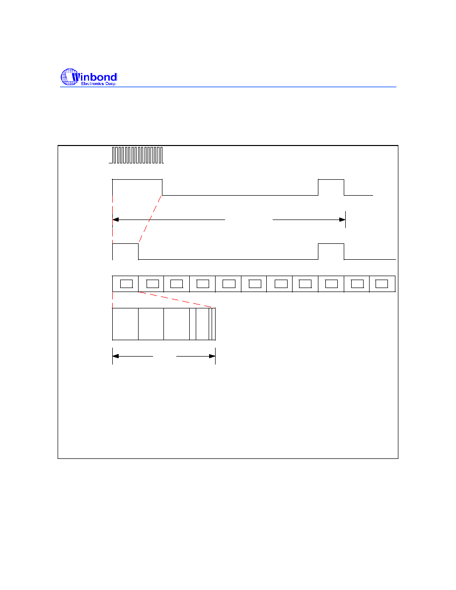
Non �TE mode timing is used LT-S and LT-T applications. The frame contains eight channel (ch0 ~
ch7) GCI channels. All structure of the eight channels shown in Fig7.11 is the same.
FSC
DU
/
DD
125us
B1 : 64 Kbits/s B channel 1
B2 : 64 Kbits/s B channel 2
M : Monitor channel
D : 16Kbits/s D channel
CI: 48Kbits/s Command / Indication Channel
A/E : 16Kbits Monitor channel handshake signaling
FSC
DCL
C0
C1
C2
C3
C4
C5
C6
C7
C0
C1
C2
B1
B2
M
D
CI
A E
C0
Fig.7.11 GCI Non �Terminal Mode Channel Structure

W6691
- 44 -
7.6.1 GCI Mode C/I Channel Handling
1) CI0 channel
The Command/Indication channel 0 carries real-time status information between the W6691 and
another device connected to the GCI bus interface.
One CI0 channel conveys the commands and indications between a layer 1 device and layer 2
device. This C/I0 channel is accessed via register CIR (in receive direction, layer 1 to layer 2) and
register CIX (in transmit direction, layer 2 to layer 1). The C/I code is 4-bit long.
� In the receive direction, the code from layer 1 is continuously monitored, with an interrupt being
generated anytime a change occurs. A new code must be found in two consecutive GCI frames
to be considered valid and to trigger a C/I code change interrupt status (double last look
criterion).
� In the transmit direction, the code written in CIX is continuously transmitted in the channel.
2) CI1 channel
CI1 channel is responsible for real time communication between W6691 and other non-layer1
peripheral devices. It consists of six bits. This channel can be used only in TE mode. C1X and C1R
are used for CI1 channel access in both of transmitting and receiving direction. CI1 code changed is
indicated by an interrupt without double last look criterion. This interrupt will set CI1 bit in GCI_EXIR.
7.6.2 GCI Mode Monitor Channel Handling
The Monitor channel protocol is a handshake protocol used for high speed information exchange
between the W6691 and other devices. The Monitor channel is necessary for:
� Programming and controlling devices attached to the GCI interface.
� Data exchange between two microprocessor systems attached to two different devices on one GCI
backplane. Use of the Monitor channel avoids the necessity of a dedicated serial communication
path between two systems.
The Monitor channel operates on an asynchronous basis. While data transfers on the bus take place
synchronized to frame sync, the flow of data is controlled by a handshake procedure using the Monitor
Channel Receiver (MOR) and Monitor Channel Transmit (MOX) bits. When data is placed into the
Monitor channel and the "A" bit is activated. This data will be transmitted repeatedly once per 8 KHz
frame until the transfer is acknowledged via the "E" bit.
The microprocessor may either enforce a 1 (idle state) in "E", "A" bit by setting the control bit MRC or
MXC (MOCR register) to 0, or enable the control of these bits internally by the W6691 according to the
Monitor channel protocol. Thus, before a data exchange can begin, the control bit MRC, or MXC
should be set to 1 by the microprocessor.
The relevant status bits are:
� For the reception of Monitor data: MDR (Monitor Channel Data Received) MER (Monitor
Channel End of Reception)
� For the transmission of Monitor data: MDA (Monitor Channel Data Acknowledged) MAB
(Monitor Channel Data Abort)

W6691
Publication Release Date: June 11, 2003
- 45 -
Revision 1.5
About the status bit MAC(Monitor Channel Transmit Active) indicates whether a transmission is
progress.
� If set MAC = 0, the previous transmission has been terminated. Before starting a transmission,
the microprocessor should verify that the transmitter is inactive.
� If set MAC = 1, after having written data into the Monitor Transmit Channel (MOX) register, the
microprocessor sets this bit to 1. This enables the "A" bit to go active (0), indicating the presence
of valid Monitor data (contents of MOX) in the corresponding frame.
The receiving device stores the Monitor byte in its MOR (Monitor Receive Channel) and generates a
MDR (Monitor Channel Data Receive) interrupt status. Alerted by the MDR interrupt, the
microprocessor reads the MOR register. When it is ready to accept data, it sets the "E" control bit
MRC to 1 to enable the receiver to store succeeding Monitor channel bytes and acknowledge them
according to the Monitor channel protocol. In addition, it enables other Monitor channel interrupts by
setting Monitor Channel Interrupt Enable to 1.
The first Monitor channel byte is acknowledged by the receiving device setting the "E" bit to 0. This
causes a MDA (Monitor Channel Data Acknowledge) interrupt status at the transmitter. A new Monitor
channel data byte can now be written by the microprocessor in MOX register. The "A" bit is still in the
active (0) state. The transmitter indicates a new byte in the Monitor channel by returning the "A" bit
active after sending it once in the inactive state. The receiver stores the Monitor channel byte in
MOR register and generates a new MDR interrupt status. When the microprocessor has read the
MOR register , the receiver acknowledges the data by returning the "E" bit active after sending it once
in the inactive state. This in turn causes the transmitter to generate a MDA interrupt status. This
MDA interrupt write data MDR interrupt read data MDA interrupt handshake procedure
is repeated as long as the transmitter has data to send.
When the last byte has been acknowledged by the receiver (MDA interrupt status), the
microprocessor sets the Monitor channel Transmit Control bit MXC to 0. This enforces an inactive (1)
state in the "A" bit. Two frames of "A" inactive signifies the end of a message. Thus, a MER (Monitor
channel End of Reception) interrupt status is generated by the receiver when the "A" bit is received in
the inactive state in two consecutive frames. As a result, the microprocessor sets the "E" bit control bit
MRC to 0, which in turn enforces an inactive state in the "E" bit. This marks the end of the
transmission, making the MAC (Monitor channel Active) bit return to 0.
During a transmission process, it is possible for the receiver to ask a transmission to be aborted by
sending an inactive "E" bit value in two consecutive frames. This is effected by the microprocessor
writing the "E" bit control bit MRC to 0. An aborted transmission is indicated by a MAB (Monitor
Channel Data Abort) interrupt
7.7 8-bit Microprocessor Interface
At power up, the reset pin RST# must be asserted to initialize the chip. At rising edge of RST#, data
value at MBS pin determines the operation modes: HIGH for Intel bus mode, LOW for Motorola bus
mode.

W6691
- 46 -
8. REGISTER DESRCRIPTIONS
8.1 D Channel HDLC Controller Register Address Map
TABLE 8.1 D CHANNEL HDLC CONTROLLER REGISTER ADDRESS MAP
OFFSET
ACCESS
REGISTER
NAME
DESCRIPTION
00
R
D_RFIFO
D channel receive FIFO
01
W
D_XFIFO
D channel transmit FIFO
02
W
D_CMDR
D channel command register
03
R/W
D_MODE
D channel mode control
04
R_clear
ISTA
Interrupt status register
05
R/W
IMASK
Interrupt mask register
06
R_clear
D_EXIR
D channel extended interrupt
07
R/W
D_EXIM
D channel extended interrupt mask
08 Reserved
09 Reserved
0A
R
D_XSTA
D channel transmit status
0B
R
D_RSTA
D channel receive status
0C Reserved
0D Reserved
0E
R/W
D_SAM
D channel address mask 1
0F
R/W
D_SAP1
D channel individual SAPI 1
10
R/W
D_SAP2
D channel individual SAPI 2
11
R/W
D_TAM
D channel address mask 2
12
R/W
D_TEI1
D channel individual TEI 1
13
R/W
D_TEI2
D channel individual TEI 2
14 Reserved
15 Reserved
16
R
D_RBCH
D channel receive frame byte count high
17
R
D_RBCL
D channel receive frame byte count low

W6691
Publication Release Date: June 11, 2003
- 47 -
Revision 1.5
8.2 GCI Bus Control Register Address Map
TABLE 8.2 GCI BUS CONTROL REGISTER ADDRESS MAP
OFFSET
ACCESS
REGISTER
NAME
DESCRIPTION
18
W
CSEL
Gci Bus cahnnel selection register
19 Reserved
1A R/W
CIR
Command/Indication
receive
1B R/W
CIX
Command/Indication
transmit
1C
R
SQR
S/Q channel receive register
1D
R/W
SQX
S/Q channel transmit register
1E Reserved
1F Reserved
20
R/W
MO0R
Monitor receive channel 0
21
R/W
MO0X
Monitor transmit channel 0
22
R_clear MO0I
Monitor channel 0 interrupt
23
R/W
MO0C
Monitor channel 0 control register
24 Reserved
25 Reserved
26
R/W
GCR
GCI mode control/ status register
27
R
MO1R
Monitor receive channel 1
28
R/W
MO1X
Monitor transmit channel 1
29
R_clear MO1I
Monitor channel 1 interrupt
2A
R/W
MO1C
Monitor channel 1 control
2B Reserved
2C Reserved
2D Reserved
2E Reserved
2F Reserved
30 Reserved
31
R
CI1R
GCI CI1 indication
32
R/W
CI1X
GCI CI1 command
33 Reserved
34
R_clear GCI_EXIR
GCI extended interrupt
35
R/W
GCI_EXIM
GCI extended interrupt mask

W6691
- 48 -
8.3 Miscellaneous Register Address Map
TABLE 8.3 MISCELLANEOUS REGISTER ADDRESS MAP
OFFSET
ACCESS
REGISTER
NAME
DESCRIPTION
36 Reserved
37 Reserved
38 R/W TIMR1
Timer
1
39 R/W TIMR2
Timer
2
3A
R/W
PCR
Peripheral control register
3B
R/W
PIODR
Peripheral I/O data register
3C
R/W
SFCTL
Switch function controll register
3D
R/W
ACTL1
Auxiliary control register 1
3E
R/W
ACTL2
Auxiliary control register 2
3F
R/W
ACTL3
Auxiliary control register 3
W6691
Publication Release Date: June 11, 2003
- 49 -
Revision 1.5
8.4 D Channel HDLC Controller Register Memory Map
TABLE 8.4 D CHANNEL HDLC CONTROLLER REGISTER MEMORY MAP
Offset
R/W
Name 7 6 5 4 3 2 1 0
00
R
D_RFIFO
01
W
D_XFIFO
02 W D_CMDR RACK RRST
0
STT1 XMS
0
XME XRST
03 R/W D_MODE
0
RACT XACT S_RLPD
0
MFD L2_DLP S_RLP
04 R_clr
ISTA
D_RMR D_RME
D_XFR INT1 INT0 D_EXI B1_EXI B2_EXI
05 R/W IMASK
D_RMR D_RME
D_XFR INT1 INT0 D_EXI B1_EXI B2_EXI
06 R_clr
D_EXIR
RDOV XDUN XCOL TIN2 GCI
ICC T1EXP SCC
07 R/W D_EXIM
RDOV XDUN XCOL TIN2 GCI
ICC T1EXP SCC
08
Reserved
09
Reserved
0A R D_XSTA
XDOW
0
XBZ
0
0
0
0
0
0B R D_RSTA
0
RDOV CRCE RMB
0
0
0
0
0C
Reserved
0D
Reserved
0E R/W
D_SAM
SAM7 SAM6 SAM5 SAM4 SAM3 SAM2 SAM1 SAM0
0F
R/W
D_SAP1 SA17 SA16 SA15 SA14 SA13 SA12 SA11 SA10
10
R/W
D_SAP2 SA27 SA26 SA25 SA24 SA23 SA22 SA21 SA20
11 R/W
D_TAM
TAM7 TAM6 TAM5 TAM4 TAM3 TAM2 TAM1 TAM0
12
R/W
D_TEI1
TA17 TA16 TA15 TA14 TA13 TA12 TA11 TA10
13
R/W
D_TEI2
TA27 TA26 TA25 TA24 TA23 TA22 TA21 TA20
14
Reserved
15
Reserved
16 R D_RBCH
VN1
VN0 LOV RBC12 RBC11 RBC10 RBC9 RBC8
17 R D_RBCL RBC7 RBC6 RBC5 RBC4 RBC3 RBC2 RBC1 RBC0
W6691
- 50 -
8.5 GCI Bus Register Memory Map
TABLE 8.5 GCI BUS REGISTER MEMORY MAP
Offset
R/W
Name 7 6 5 4 3 2 1 0
18
R/W
CSEL
0 0 0 0 0
CSEL2
CSEL1
CSEL0
19
Reserved
1A
R
CIR
0 0 0
BAS
CORD3 CORD2
CORD1 CORD0
1B
R/W
CIX
0 0 0
BAC
CORD3 CORD2
CORD1 CORD0
1C R SQR
0
0 MSYN 0
S1 S2 S3 S4
1D R/W
SQX
0 0 0 0 Q1
Q1
Q1
Q1
1E
Reserved
1F
Reserved
20 R MO0R
21 R/W MO0X
22 R_clr
MO0I
0 0 0 0
MDR0
MER0
MDA0
MAB0
23 R/W MO0C
0 0 0 0
MRIE0
MRC0
MXIE0
MXC0
24
Reserved
25
Reserved
26 R GCR
MAC0
MAC1
0 0 0 0 0 0
27 R MO1R
28 R/W MO1X
29 R_clr
MO1I
0 0 0 0
MDR1
MER1
MDA1
MAB1
2A R/W
MO1C
0 0 0 0
MRIE1
MRC1
MXIE1
MXC1
2B
Reserved
2C
Reserved
2D
Reserved
2E
Reserved
2F
Reserved
30
Reserved
31 R CI1R
0 0
CI1R_6
CI1R_5
CI1R_4 CI1R_3
CI1R_2 CI1R_1
32 R/W CI1X
0
0
CI1X_6 CI1X_5 CI1X_4 CI1X_3 CI1X_2 CI1X_1
33
Reserved
34 R_clr
GCI_EXIR
0 0 0
MO1C
MO0C
0 0 CI1
35 R/W GCI_EXIM
1 1 1
MO1C
0 0 0 CI1
W6691
Publication Release Date: June 11, 2003
- 51 -
Revision 1.5
8.6 Miscellaneous Register Memory Map
TABLE 8.6 MISCELLANEOUS REGISTER MEMORY MAP
Offset
R/W
Name 7 6 5 4 3 2 1 0
36
Reserved
37
Reserved
38 R/W
TIMR1
T1MD CNT6 CNT5 CNT4 CNT3 CNT2 CNT1 CNT0
39 R/W
TIMR2
TMD TIDLE TCN5 TCN4 TCN3 TCN2 TCN1 TCN0
3A
R/W
PCR
0 0 0 0
OE3
OE2
OE1
OE0
3B
R/W
PIODR 0 0 0 0 IO3
IO2
IO1
IO0
3C R/W SFCTL
0 PGSWH PCRLP PXC B2SW1 B2SW0 B1SW1 B1SW0
3D
R/W
ACTL1
0 0 SRST 0 0 0 OPS1
OPS0
3E R/W ACTL2
0
ACTL1 LC
0
SPU
0
0
0
3F
R/W
ACTL3 0
INTOL
0 0 0 0 0 0
8.7 D Channel HDLC Controller Register Description
8.7.1 D_ch receive FIFO
D_RFIFO
Read Address 00H
The D_RFIFO has a length of 64 bytes.
After a D_RMR interrupt, exactly 32 bytes are available.
After a D_RME interrupt, the number of bytes available equals RBC4-0 bits in the D_RBCL register.
8.7.2 D_ch transmit FIFO
D_XFIFO
Write Address 01H
The D_XFIFO has a length of 64 bytes.
After an D_XFR interrupt, up to 32 bytes of data can be written into this FIFO for transmission. At the
first time transmission, up to 64 bytes of data can be written.
8.7.3 D_ch command register
D_CMDR
Write Address 02H
Value after reset: 00H
7 6 5 4 3 2 1 0
RACK
RRST 0 STT1
XMS 0 XME
XRST

W6691
- 52 -
RACK Receive Acknowledge
After a D_RMR or D_RME interrupt, the processor must read out the data in D_RFIFO and then sets
this bit to acknowledge the interrupt. Writing "0" to this bit has no effect. If RACK bit is set to "1" for
operating "Receiver Acknowledge", It is not necessary to reset RACK bit to "0" by host processor.
That is to say, once RACK is set to "1", RACK bit is reset to "0" by W6691 automatically.
RRST Receiver Reset
Setting this bit resets the D_ch HDLC receiver and clears the D_RFIFO data. Writing "0" to this bit has
no effect. If RRST bit is set to "1" for operating "Receiver Reset", It is not necessary to reset RRST bit
to "0" by host processor. That is to say, once RRST is set to "1", RRST bit is reset to "0" by W6691
automatically.
STT1 Start Timer 1
The timer 1 is started when this bit is set to one. The timer is stopped when it expires or by a write of
the TIMR1 register. Writing "0" to this bit has no effect. If SST1 bit is set to "1" for operating "Start
Timer1", It is not necessary to reset STT1 bit to "0" by host processor. That is to say, once STT1 is set
to "1", STT1 bit is reset to "0" by W6691 automatically.
XMS Transmit Message Start/Continue
Setting this bit will start or continue the transmission of a frame. The opening flag is automatically
added by the HDLC controller. Writing "0" to this bit has no effect. If XMS bit is set to "1" for operating
"Transmit Message Start/Continue", It is not necessary to reset XMS bit to "0" by host processor. That
is to say, once XMS is set to "1", XMS bit is reset to "0" by W6691 automatically.
XME Transmit Message End
Setting this bit indicates the end of frame transmission. The D_ch HDLC controller automatically
appends the CRC and the closing flag after the data transmission. Writing "0" to this bit has no effect.
If XME bit is set to "1" for operating "Transmit Message End", It is not necessary to reset XME bit to
"0" by host processor. That is to say, once XME is set to "1", XME bit is reset to "0" by W6691
automatically.
Note: If the frame
32 bytes, XME plus XMS commands must be issued at the same time.
XRST Transmitter Reset
Setting this bit resets the D_ch HDLC transmitter and clears the D_XFIFO. The transmitter will send
inter frame time fill pattern (which is 1's) immediately. This command also results in a transmit FIFO
ready condition. Writing "0" to this bit has no effect. If XRST bit is set to "1" for operating "Transmit
Reset", It is not necessary to reset XME bit to "0" by host processor. That is to say, once XRST is set
to "1", XRST bit is reset to "0" by W6691 automatically.

W6691
Publication Release Date: June 11, 2003
- 53 -
Revision 1.5
8.7.4 D_ch Mode Register D_MODE
Read/Write
Address 03H
Value after reset: 00H
7 6 5 4 3 2 1 0
0 RACT
XACT 0
S_RLPD
MFD
L2_DLP S_RLP
RACT Receiver Active
Setting this bit activates the D_ch HDLC receiver. This bit can be read. The receiver must be in active
state in order to receive data.
Note: The receiver is deactive after hardware reset or software reset.
XACT Transmitter Active
Setting this bit activates the D_ch HDLC transmitter. This bit can be read. The transmitter must be in
active state in order to transmit data.
Note: The transmitter is deactive after hardware reset or software reset.
S_RLPD S Interface Remote Loopback with D channel Loopback
Setting this bit to "1" activates the remote loopback function. The received 2B channels from the S
interface are looped to the transmitted 2B channels of S interface. The received D channel from the S
interface is also looped to transmitted D channel of S interface in the loopback function.
MFD Multiframe Disable
This bit is used to enable or disable the multiframe structure on S/T interface:
0: Multiframe is enabled
1: Multiframe is disabled
L2_DLP Layer2 Digital Loopback
Setting this bit activates the layer2 digital loopback function. The transmitted digital 2B+D channels
are looped to the received 2B+D channels. Note that after hardware reset, the internal clocks will turn
off if the S bus is not connected or if there is no signal on the S bus. In this case, the C/I command
ECK must be issued to enable loopback function.
S_RLP S Interface Remote Loopback
Setting this bit to "1" activates the remote loopback function. The received 2B channels from the S
interface are looped to the transmitted 2B channels of S interface. The received D channel from the S
interface is not looped to transmitted D channel of S interface in this loopback function.

W6691
- 54 -
8.7.5 Interrupt Status Register
ISTA
Read_clear
Address 04H
Value after reset: 00H
7 6 5 4 3 2 1 0
D_RMR D_RME D_XFR INT1
INT0 D_EXI B1_EXI B2_EXI
D_RMR D_ch Receive Message Ready
A 64-byte data is available in the D_RFIFO. The frame is not complete yet.
D_RME D_ch Receive Message End
The last part of a frame with length > 32 bytes or a whole frame with length
32 bytes has
been received. The whole frame length is obtained from D_RBCH + D_RBCL registers. The length of
data in the D_RFIFO equals:
data length = RBC4-0 if RBC4-0
0
data length = 32 if RBC4-0 = 0
D_XFR D_ch Transmit FIFO Ready
This bit indicates that the transmit FIFO is ready to accept data. Up to 32 bytes of data can be written
into the D_XFIFO.
An D_XFR interrupt is generated in the following cases:
- Ater an XMS command, when
32 bytes of XFIFO is empty
- After an XMS together with an XME command is issued, when the whole frame has been
transmitted
- After an XRST command
- After hardware reset or software reset
INT1 INT1 Interrupt
If the INT1 bit is set to "1", this bit indicates that interrupt trigger occurs at INT1 pin.
INT0 INT0 Interrupt
If the INT0 bit is set to "1", this bit indicates that interrupt trigger occurs at INT0 pin.
D_EXI D_ch Extended Interrupt
This bit indicates that at least one interrupt bit is set in D_EXIR register.
Note: A read of the ISTA register clears all bits except D_EXI, D_EXI bit is cleared when all bits in
D_EXIR register are cleared.
B1_EXI B1_ch Extended Interrupt
This bit indicates that at least one interrupt bit has been set in B1_EXIR register.

W6691
Publication Release Date: June 11, 2003
- 55 -
Revision 1.5
B2_EXI B2_ch Extended Interrupt
This bit indicates that at least one interrupt bit has been set in B2_EXIR register.
8.7.6 Interrupt Mask Register
IMASK Read/Write
Address 05H
Value after reset: FFH
7 6 5 4 3 2 1 0
D_RMR D_RME D_XFR INT1
INT0 D_EXI B1_EXI B2_EXI
Setting the bit to "1" masks the corresponding interrupt source in ISTA register. Masked interrupt
status bits are read as zero. They are internally stored and pending until the mask bits are zero.
Note: Setting the D_EXI bit to "1" masks the interrupts in D_EXIR register.
8.7.7 D_ch Extended Interrupt Register D_EXIR
Read_clear
Address 06H
Value after reset: 00H
7 6 5 4 3 2 1 0
RDOV XDUN XCOL TIN2 GCI ICC T1EXP SCC
RDOV Receive Data Overflow
Frame overflow (too many short frames) or data overflow occurs in the receive FIFO. In data overflow,
the incoming data will overwrite the data in the receive FIFO. If RDOV interrupt occurs, software has
to reset the receiver and discard the data received.
XDUN Transmit Data Underrun
This interrupt indicates the D_XFIFO has run out of data. In this case, the W6691 will automatically
reset the transmitter and send the inter frame time fill pattern (all 1's) on D channel. The
microprocessor must wait until transmit FIFO ready (via XFR interrupt), re-write data, and issue XMS
command to re-transmit the data.
XCOL Transmit Collision
This bit indicates a collision on the S-bus has been detected. W6691 will automatically reset the
transmitter and software must wait until transmit FIFO ready (via XFR interrupt), then, re-write data,
and issue XMS command to re-transmit the data.
TIN2 Timer 2 Expiration
This bit is set when Timer 2 counts down to zero.
GCI GCI Interrupt
This bit is set when at least one bit is set in GCI_EXIR register.
ICC Indication Channel Change

W6691
- 56 -
A change in the layer 1 indication code is detected. The actual value can be read from CIR registers.
T1EXP Timer 1 Expiration
Expiration occurs in the Timer 1.
SCC S Channel Change
A change in multi-frame S channel is detected. The actual value can be read from SQR registers.
8.7.8 D_ch Extended Interrupt Mask Register
D_EXIM Read/Write Address 07H
Value after reset: FFH
7 6 5 4 3 2 1 0
RDOV XDUN XCOL TIN2 GCI ICC T1EXP
SCC
Setting the bit to "1" masks the corresponding interrupt source in D_EXIR register. Masked interrupt
status bits are read as zero. They are internally stored and pending until the mask bits are zero.
Note: All the interrupts in D_EXIR will be masked if the IMASK:D_EXI bit is set to "1".
8.7.9 D_ch Transmitter Status Register D_XSTA
Read
Address
0AH
Value after reset: 00H
7 6 5 4 3 2 1 0
XDOW
0
XBZ
0 0 0 0 0
XDOW Transmit Data Overwritten
At least one byte of data has been overwritten in the D_XFIFO. This bit is set by data overwritten
condition and is cleared only by XRST command.
XBZ Transmitter Busy
This bit indicates the D_HDLC transmitter is busy. The XBZ bit is set to"1" from the transmission of
opening flag to the transmission of closing flag.
8.7.10 D_ch Receive Status Register
D_RSTA
Read
Address 0BH
Value after reset: 20H
7 6 5 4 3 2 1 0
0
RDOV
CRCE
RMB
0 0 0 0
RDOV Receive Data Overflow
A "1" indicates that the D_RFIFO is overflow. The incoming data will overwrite data in the receive
FIFO. The data overflow condition will set both the status and interrupt bits. It is recommended that
software must read the RDOV bit after reading data from D_RFIFO when RMR or RME interrupt

W6691
Publication Release Date: June 11, 2003
- 57 -
Revision 1.5
occurs. The software must abort the data and issue a RRST command to reset the receiver if RDOV
= 1. The frame overflow condition will not set this bit.
CRCE CRC Error
This bit indicates the result of frame CRC check:
0: CRC correct
1: CRC error
RMB Receive Message Aborted
A "1" means that a sequence of seven 1's was received and the frame is aborted. Software must
issue RRST command to reset the receiver.
Note: Normally D_RSTA register should be read by the microprocessor after a D_RME interrupt. The contents of D_RSTA are
valid only after a D_RME interrupt and remain valid until the frame is acknowledged via a RACK bit.
8.7.11 D_ch SAPI Address Mask D_SAM
Read/Write
Address 0EH
Value after reset: 00H
7 6 5 4 3 2 1 0
SAM7 SAM6 SAM5 SAM4 SAM3 SAM2 SAM1 SAM0
This register masks(disables) the first byte address comparison of the incoming frame. If the mask bit
is "1" the corresponding bit comparisons with D_SAP1, D_SAP2 are disabled. Comparison with SAPG
is always performed.
Each HDLC frame has two address byte. The first byte is SPAI and second byte is TEI. The D_ch
HDLC controller will compare these two bytes with contents of D_SAPI1, DSAP2 and D_TEI1,
D_TEI2. If the HDLC frame SAPI matches D_SAPI1 or D_SAP2 and the HDLC frame TEI matches
D_TEI1 or D_TEI2, the HDLC frame is captured and stored in D_channel receiving FIFO. If
comparison operation is enabled (This means that the more than one bit in D_SAM is set to "1"),
except the frame with matching address is stored, others are discarded. If comparison operation is
disabled (This means that the all bits in D_SAM are set to "0"), all frame with any address combination
are captured and stored in receiving FIFO. The mask operation can be programmed by each bit
respectively. The HDLC frame with SAPG and /or TEIG address are always captured and stored.
Note: For the LAPD frame, the least significant two bits are the C/R bit and EA = 0 bit. It is suggested that the comparison with
C/R bit be masked. EA = 0 for two octet address frame e.g LAPD, EA = 1 for one octet address frame.

W6691
- 58 -
8.7.12 D_ch SAPI1 Register D_SAP1
Read/Write
Address 0FH
Value after reset: 00H
7 6 5 4 3 2 1 0
SA17 SA16 SA15 SA14 SA13 SA12 SA11 SA10
This register contains the first choice of the first byte address of received frame. For LAPD frame,
SA17 - SA12 is the SAPI value, SA11 is C/R bit and SA10 is zero.
8.7.13 D_ch SAPI2 Register
D_SAP2
Read/Write
Address 10H
Value after reset: 00H
7 6 5 4 3 2 1 0
SA27 SA26 SA25 SA24 SA23 SA22 SA21 SA20
This register contains the second choice of the first byte address of received frame. For LAPD frame,
SA27 - SA22 is the SAPI value, SA21 is C/R bit and SA20 is zero.
8.7.14 D_ch TEI Address Mask
D_TAM
Read/Write
Address 11H
Value after reset: 00H
7 6 5 4 3 2 1 0
TAM7 TAM6 TAM5 TAM4 TAM3 TAM2 TAM1 TAM0
This register masks (disables) the second byte address comparison of the incoming frame. If the
mask bit is "1" the corresponding bit comparisons with D_TEI1, D_TEI2 are disabled. The HDLC
frame with SAPG and /or TEIG address are always captured and stored.
Note: For the LAPD frame, the least significant bit is the EA =1 bit.
8.7.15 D_ch TEI1 Register D_TEI1 Read/Write
Address 12H
Value after reset: 00H
7 6 5 4 3 2 1 0
TA17 TA16 TA15 TA14 TA13 TA12 TA11 TA10
TA17 - TA10
This register contains the first choice of the second byte address of received frame. For LAPD frame,
TA17 - TA11 is the TEI value, TA10 is EA = 1.

W6691
Publication Release Date: June 11, 2003
- 59 -
Revision 1.5
8.7.16 D_ch TEI2 Register D_TEI2 Read/Write
Address 13H
Value after reset: 00H
7 6 5 4 3 2 1 0
TA27 TA26 TA25 TA24 TA23 TA22 TA21 TA20
TA27 - TA20
This register contains the second choice of the second byte address of received frame. For LAPD
frame, TA27 - TA21 is the TEI value, TA20 is EA = 1.
8.7.17 D_ch Receive Frame Byte Count High
D_RBCH
Read Address 16H
Value after reset: 40H
7 6 5 4 3 2 1 0
VN1 VN0 LOV
RBC12
RBC11 RBC10
RBC9
RBC8
VN1-0 Chip Version Number
This is the chip version number. It is read as 01B.
LOV Length Overflow
A "1" in this bit indicates
8192 bytes are received and the frame is not yet complete. This bit is valid
only after a D_RME interrupt and remains valid until the frame is acknowledge via the RACK
command.
RBC12-8 Receive Byte Count
These bits are five most significant bits of the total frame length. These bits are valid only after a
D_RME interrupt and remain valid until the frame is acknowledge via the RACK command.
8.7.18 D_ch Receive Frame Byte Count Low
D_RBCL Read
Address 17H
Value after reset: 00H
7 6 5 4 3 2 1 0
RBC7 RBC6 RBC5 RBC4 RBC3 RBC2 RBC1 RBC0
RBC7-0 Receive Byte Count
These bits are eight least significant bits of the total frame length. Bits RBC4-0 also indicate the length
of the data currently available in D_RFIFO. These bits are valid only after an D_RME interrupt and
remain valid until the frame is acknowledged via the RACK command.

W6691
- 60 -
8.8 GCI Bus Register Description
8.8.1 Channel Selection Register
CSEL
Read/Write
Address 18H
Value after reset: 00H
7 6 5 4 3 2 1 0
0 0 0 0 0
CSEL2 CSEL1 CSEL0
CSEL2, CSEL1 and CSEL0 define W6691 locating in GCI channel number operated in LT-S/ LT-T
mode.
8.8.2 Command/Indication Receive Register CIR
Read
Address
1AH
Value after reset: 0FH
7 6
5
4 3 2 1 0
0
0
0
BAS CODR3 CODR2 CODR1 CODR0
BAS Bus Access Status
Indicate the state of the TIC �bus:
1: W6691 itself occupies the D and C/I channel.
0: Another device occupies the D channel and C/I channel.
CODR3-0 Layer 1 Indication Code
Value of the received layer 1 indication code. Note these bits have a buffer size of two. If TE mode is
selected, CODR3-0 bits are CI0 bits in GCI bus channel.
8.8.3 Command/Indication Transmit Register
CIX
Read/Write
Address 1BH
Value after reset: 0FH
7 6 5 4 3 2 1 0
0 0 0
BAC
CODX3 CODX2 CODX1 CODX0
BAC Bus Access Control
It is available if TIC bus function is active. If this bit is set to "1", W6691 will try to access the TIC-bus
to occupy the C/I channel even if no D channel frame has to be transmitted. It should be reset when
the access has been completed to grant a similar access to the other devices transmitting in that GCI
channel.

W6691
Publication Release Date: June 11, 2003
- 61 -
Revision 1.5
CODX3-0 Layer 1 Command Code
Value of the command code is transmitted to layer 1. If TE mode is selected, CODX3-0 bits are CI0 bit
in GCI bus channel.
Reading this register returns the previous written value.
8.8.4 S/Q Channel Receive Register
SQR Read Address 1CH
Value after reset: XXH
7 6 5 4 3 2 1 0
0 0 MSYN 0 S1 S2 S3 S4
MSYN Multiframe Synchronization
When this bit is "1", a multiframe synchronization is achived, i.e the S/T receiver has synchronized to
the received F
A
and M bit patterns.
S1-4 Received S Bits
These are the S bits received in NT to TE direction in frames 1, 6, 11 and 16. S1 is in frame 1, S2 is in
frame 6 etc. These four bits are double buffered.
8.8.5 S/Q Channel Transmit Register
SQX Read/Write Address 1DH
Value after reset: 0FH
7 6 5 4 3 2 1 0
0 0 0 0 Q1
Q2
Q3
Q4
Q1-4 Transmitted Q Bits
These are the transmitted Q channels in F
A
bit positions in frames 1, 6, 11 and 16. Q1 is in frame 1
and Q2 is in frame 6 etc.
Reading this register returns the previous written value.
8.8.6 Monitor Receive Channel 0
MO0R Read Address 20H
Value after reset: FFH
7 6 5 4 3 2 1 0
Contains the Monitor channel data received in GCI Monitor channel 0 according to the Monitor
channel protocol.

W6691
- 62 -
8.8.7 Monitor Transmit Channel 0 MO0X
Read/Write
Address
21H
Value after reset: FFH
7 6 5 4 3 2 1 0
Contains the Monitor channel data transmitted in GCI Monitor channel 0 according to the Monitor
channel protocol.
8.8.8 Monitor Channel 0 Interrupt Register
MO0I Read_clear Address 22H
Value after reset: 00H
7 6 5 4 3 2 1 0
0 0 0 0
MDR0
MER0
MDA0
MAB0
MDR0 Monitor channel 0 Data Receive
MER0 Monitor channel 0 End of Reception
MDA0 Monitor channel 0 Data Acknowledged
The remote end has acknowledged the Monitor byte being transmitted.
MAB0 Monitor channel 0 Data Abort
8.8.9 Monitor Channel 0 Control Register MO0C
Read/Write
Address 23H
Value after reset: 00H
7 6 5 4 3 2 1 0
0 0 0 0
MRE0
MRC0
MIE0
MXC0
MRE0 Monitor Channel 0 Receive Interrupt Enable
Monitor channel interrupt status MDR0, MER0 generation is enabled (1) or masked (0).
MRC0 "E" Bit Control
Determines the value of the "E" bit:
0: "E" bit always "1". In addition, the MDR0 interrupt is blocked, except for the first byte of a packet (if
MRE0 = 1).
1: "E" bit is internally controlled by the W6691 according to Monitor channel protocol.
In addition, the MDR0 interrupt is enabled for all received bytes according to the Monitor channel
protocol (if MRE0 = 1).

W6691
Publication Release Date: June 11, 2003
- 63 -
Revision 1.5
MIE0 Monitor channel 0 Transmit Interrupt Enable
Monitor interrupt status MDA0, MAB0 generation is enabled (1) or masked (0).
MXC0 "A" bit Control
Determines the value of the "A" bit:
0: "A" bit is always 1.
1: "A" bit is internally controlled by W6691 according to Monitor channel protocol.
8.8.10 GCI Mode Control/Status Register
GCR Read
Address 26H
Value after reset: 00H
7 6 5 4 3 2 1
0
MAC0 MAC1 0
0
0
0 0 0
MAC0 Monitor Transmit Channel 0 Active (Read Only)
Data transmission is in progress in GCI mode Monitor channel 0.
0: the previous transmission has been terminated. Before starting a transmission, the microprocessor
should verify that the transmitter is inactive.
1: after having written data into the Monitor Transmit Channel 0 (MO0X) register, the microprocessor
sets this bit to 1.
This enables the "A" bit to go active (0), indicating the presence of valid Monitor channel data
(contents of MOX) in the corresponding frame.
MAC1 Monitor Transmit Channel 1 Active (Read Only)
Data transmission is in progress in GCI mode Monitor channel 1.
0: the previous transmission has been terminated. Before starting a transmission, the microprocessor
should verify that the transmitter is inactive.
1: after having written data into the Monitor Transmit Channel 1 (MO1X) register, the microprocessor
sets this bit to 1.
This enables the "A" bit to go active (0), indicating the presence of valid Monitor channel data
(contents of MOX) in the corresponding frame.
8.8.11 Monitor Receive Channel 1 Register MO1R
Read Address 27H
Value after reset: FFH
7 6 5 4 3 2 1 0
Contains the Monitor channel data received in GCI Monitor channel 1 according to the Monitor
channel protocol.

W6691
- 64 -
8.8.12 Monitor Transmit Channel 1 Register
MO1X Read/Write Address 28H
Value after reset: FFH
7 6 5 4 3 2 1 0
Contains the Monitor channel data transmitted in GCI Monitor channel 1 according to the Monitor
channel protocol.
8.8.13 Monitor Channel 1 Interrupt Register
MO1I Read_clear Address 29H
Value after reset: 00H
7 6 5 4 3 2 1 0
0 0 0 0
MDR1
MER1
MDA1
MAB1
MDR1 Monitor channel 1 Data Receive
MER1 Monitor channel 1 End of Reception
MDA1 Monitor channel 1 Data Acknowledged
The remote end has acknowledged the Monitor byte being transmitted.
MAB1 Monitor channel 1 Data Abort
8.8.14 Monitor Channel 1 Control Register MO1C
Read/Write
Address 2AH
Value after reset: 00H
7 6 5 4 3 2 1 0
0 0 0 0
MRE1
MRC1
MIE1
MXC1
MRE1 Monitor Channel 1 Receive Interrupt Enable
Monitor channel interrupt status MDR1, MER1 generation is enabled (1) or masked (0).
MRC1 "E" Bit Control
Determines the value of the "E" bit:
0: "E" bit is always 1. In addition, the MDR1 interrupt is blocked, except for the first byte of a packet
(if MRE1 = 1).
1: "E" bit is internally controlled by the W6691 according to Monitor channel protocol. In addition, the
MDR1 interrupt is enabled for all received bytes according to the Monitor channel protocol (if
MRE1=1).

W6691
Publication Release Date: June 11, 2003
- 65 -
Revision 1.5
MIE1 Monitor channel 1 Transmit Interrupt Enable
Monitor interrupt status MDA1, MAB1 generation is enabled (1) or masked (0).
MXC1 "A" bit Control
Determines the value of the "A" bit:
0: "A" bit isalways 1.
1: "A" bit internally controlled by the W6691 according to Monitor channel protocol.
8.8.15 GCI CI1 Indication Register
CI1R
Read
Address
31H
Value after reset: Undefined
7 6 5 4 3 2 1 0
0 0
CI1R_6 CI1R_5 CI1R_4 CI1R_3 CI1R_2 CI1R_1
CI1R_6-1
Input data of GCI CI1 channel. CI1R is only used in TE mode selected.
Example application is data of ARCOFI's Peripheral Control Interface input pins.
8.8.16 GCI CI1 Command Register
CI1X
Read/Write
Address 32H
Value after reset: 3FH
7 6 5 4 3 2 1 0
0 0
CI1X_6
CI1X_5
CI1X_4 CI1X_3 CI1X_2 CI1X_1
CI1X6_1
Transmitted data of GCI CI1 channel. CI1R is only used in TE mode selected. A read to these bits
returns the previously written value.
Example application is data of ARCOFI's Peripheral Control Interface output pins.
8.8.17 GCI Extended Interrupt Register
GCI_EXIR
Read_clear
Address 34H
Value after reset: 00H
7 6 5 4 3 2 1 0
0 0 0
MO1C
MO0C
0 0 CI1
MO1C Monitor Channel 1 Status Change
A change in the Monitor Channel 1 Interrupt register (MO1I) has occurred. A new Monitor channel
byte is stored in the MO1R register.

W6691
- 66 -
MO0C Monitor Channel 0 Status Change
A change in the Monitor Channel 0 Interrupt register (MO0I) has occurred. A new Monitor channel
byte is stored in the MO0R register.
CI1 CI1 Synchronous Transfer Interrupt
When enabled, an interrupt is generated when there is a change in the received CIR1_6-1 code
without double last look criterion. It is only used in TE-mode.
8.8.18 GCI Extended Interrupt Mask Register GCI_EXIM Read/Write Address 35H
Value after reset: F7H
7 6 5 4 3 2 1 0
1 1 1
MO1C
0 0 0 CI1
Bit 7-5 are fixed at "1" and bit 3 is fixed at '0". This means MO0C interrupt cannot be masked. The
interrupt is disabled when the bit is set.
8.9 Miscellaneous Register
8.9.1 Timer 1 Register
TIMR1
Read/Write
Address 38H
Value after reset: 00H
7 6 5 4 3 2 1 0
T1MD CNT6 CNT5 CNT4 CNT3 CNT2 CNT1 CNT0
T1MD Timer1 Mode
0 = Single Count Down Mode: The timer counts once and generates a T1EXP interrupt when expires.
1 = Periodical Count Down Mode: The timer counts periodically and generates an T1EXP interrupt at
each expiration.
CNT6-0 Count Value
The expiration time is defined as:
T1 = CNT[6:0] * 0.1 second
After writing this register, STT1 bit in D_CMDR register must be set to start the timer. This register can
be read only after the timer has been started. The read value indicates the timer's current count value.
In case layer 1 is not activated, a C/I command "ECK" must be issued in addition to the STT1
command to start the timer.
Note: The timer is stopped when it expires in Single Count Down Mode(T1MD = 0) or TIMR1 register is re-written in both mode.

W6691
Publication Release Date: June 11, 2003
- 67 -
Revision 1.5
8.9.2 Timer 2
TIMR2
Read/ Write Address
39H
Value after reset: 00H
7 6 5 4 3 2 1 0
TMD TIDLE TCN5 TCN4 TCN3 TCN2 TCN1 TCN0
TMD Timer 2 Mode
0: Single Count Down mode: The timer starts when it is written a non-zero count value and stops
when it reaches zero.
1: Periodical Count Down Mode: The timer starts when it is written a non-zero count value and counts
down cyclically (periodically) with the count value.
In both cases, a maskable interrupt TIN2 is generated every time the timer reaches zero. When timer
starts, pin TOUT2 changes to HIGH and toggles every half count time. Therefore, the period of
TOUT2 equals count value.
In both cases, timer counts with the new value if it is written again before expiration.
The timer is stopped when it expires in single count mode (TMD = 0), or zero count value is written in
TCN5-0 (TMD = 0 or 1).
TIDLE TOUT2 Idle
This bit defines value of TOUT2 pin when timer is off. That is to say, the TIDLE determine the TOUT2
pin level is high or low when timer2 is off.
TCN5-0 Timer 2 Count Value
0: Timer is off.
1 - 63: Timer count value in unit of ms.
8.9.3 Peripheral Control Register PCR Read/Write
Address 3AH
Value after reset: 00H
7 6 5 4 3 2 1 0
0 0 0 0
OE3
OE2
OE1
OE0
Only for PLCC 68 pins:
OE3 Direction Control for IO3
0: Pin IO3's output driver is disabled and input driver is enabled
1: Pin IO3's output driver is enabled.
Note: The ACLT2: INT1M bit should be set to "0", INT1/IO3 pin can be as IO. Otherwise, It is configured as interrupt input.

W6691
- 68 -
OE2 Direction Control for IO2
0: Pin IO2's output driver is disabled and input driver is enabled
1: Pin IO2's output driver is enabled.
Note: The ACLT2: INT0M bit should be set to "0", INT0/IO2 pin can be as IO. Otherwise, It is configured as interrupt input.
OE1 Direction Control for IO1
0: Pin IO1's output driver is disabled and input driver is enabled
1: Pin IO1's output driver is enabled.
OE0 Direction Control for IO0
0 : Pin IO0's output driver is disabled and input driver is enabled
1: Pin IO0's output driver is enabled.
8.9.4 Peripheral I/O Data Register PIODR
Read/Write
Address 3BH
Value after reset: 00
7 6 5 4 3 2 1 0
0 0 0 0 IO3
IO2
IO1
IO0
Only for PLCC 68 pins:
IO3 Read or Write Data of Pin IO3
On read operation, the present value of pin IO3 is read.
On write operation, the data is driven to pin IO3 only if PCTL:OE3=1.
Note: The ACLT2: INT1M bit should be set to "0", INT1/IO3 pin can be as IO. Otherwise, It is configured as interrupt input.
IO2 Read or Write Data of Pin IO2
On read operation, the present value of pin IO2 is read.
On write operation, the data is driven to pin IO2 only if PCTL:OE2=1.
Note: The ACLT2: INT0M bit should be set to "0", INT0/IO2 pin can be as IO. Otherwise, It is configured as interrupt input.
IO1 Read or Write Data of Pin IO1
On read operation, the present value of pin IO1 is read.
On write operation, the data is driven to pin IO1 only if PCTL:OE1=1.
IO0 Read or Write Data of Pin IO0
On read operation, the present value of pin IO0 is read.
On write operation, the data is driven to pin IO0 only if PCTL:OE0=1.
W6691
Publication Release Date: June 11, 2003
- 69 -
Revision 1.5
8.9.5 SFCTL Switch Functional Control Register Read/Write
Address 3CH
Value after reset: 00H
7 6 5 4 3 2 1 0
0
PGSWH PCRLP PXC B2SW1 B2SW0 B1SW1 B1SW0
PGSWH PCM and GCI bus Switch
Determines the CODEC interface is to be operated in B channel.
1: PCM bus is selected to operate with CODEC.
0: GCI bus is selected to operate with CODEC.
PCRLP PCM Remote Loop Back
Setting this bit activates the PCM channel remote loopback function. The transmitted PCM data to
PCM channel are looped to received PCM channel.
PXC PCM Cross-connect
This bit determines whether or not the PCM ports are cross-connected with the B channel ports. The
setting of PXC is independent of the BSW1-0 bits.
PXC Connection
0
PCM1
B1, PCM2 B2
1
PCM1
B2, PCM2 B1
B2SW1/B2SW0 B2 channel Switch
These two bits determine B2 channel switch among PCM port, GCI and Layer2.
00: Select B2 channel switch between Layer2 and Layer1/GCI.
01: Select B2 channel switch between Layer1/GCI and PCM.
10: Select B2 channel switch between PCM and Layer2.
B1SW1 / B1SW0 B1 channel Switch
These two bits determine B1 channel switch among PCM port, GCI and Layer2.
00: Select B1 channel switch between Layer2 and Layer1/GCI.
01: Select B1 channel switch between Layer1/GCI and PCM.
10: Select B1 channel switch between PCM and Layer2.
W6691
- 70 -
8.9.6 ACTL1 Auxiliary Control Register 1
Read/Write
Address 3DH
Value after reset: 00H
7 6 5 4 3 2 1 0
0 0
SRST
0 0 0
OPS1
OPS0
SRST Software Reset
When this bit is set to "1" 1ms at least, a software reset signal is activated. The effect of the reset
signal is same as the hardware reset.
This bit is not auto-clear, the software must write "0" to this bit to exit from the reset mode.
Note: When SRST = 1, the chip is in reset state. Read or write to any of the registers is inhibited at
this moment.
OPS1-0 Output Phase Delay Compensation Select1-0
These two bits select the output phase delay compensation.
OPS1 OPS0
EFFECT
0
0
No output phase delay compensation
0
1
Output phase delay compensation 260nS
1
0
Output phase delay compensation 520 nS
1
1
Output phase delay compensation 1040 nS
8.9.7 ACTL2 Auxiliary Control Register2 Read/Write
Address 3EH
Value after reset: 40H
7 6 5 4 3 2 1 0
0
ACTL1S
LC 0 SPU 0 0 0
ACLT1S
Activate Layer1 Status
0: When Layer 1 operates in activate state, ACTL1S pin is pulled to low level. In contrast, if Layer 1
operates in deactivate state, ACTL1S pin is driven to high level.
1: The ACTL1 output level is programmed by microprocessor.(ACTL2 : ACLT1S)
LC LED Controlled
If ACLTS1is set to "1", LC bit is programmable by microprocessor.
0: It shows ACTLS1 pin is driven to high level.
1: It shows ACTLS1 pin is driven to low level.
SPU: Software Power UP
If SPU is set to "1", W6691 can awaked from power down mode.

W6691
Publication Release Date: June 11, 2003
- 71 -
Revision 1.5
8.9.8 ACTL3 Auxiliary Control Register 3
Read/Write
Address 3FH
Value after reset: 00H
7 6 5 4 3 2 1 0
0
INTOL
0 0 0 0 0 0
INTOL Interrupt
Output Level Configuration
0: It shows INT pin is low active (open drain).
1: It shows INT pin is high active.
8.10 B1 Channel HDLC Controller Register Address MAP
TABLE 8.7 B1 CHANNEL HDLC CONTROLLER REGISTER ADDRESS MAP
Offset Access Register
Name
Description
50
R
B1_RFIFO
B1 channel receive FIFO
51
W
B1_XFIFO
B1 channel transmit FIFO
52 Reserved
53
R/W
B1_CMDR
B1 channel command register
54
R/W
B1_MODE
B1 channel mode control
55 Reserved
56
R_clear B1_EXIR
B1 channel extended interrupt
57
R/W
B1_EXIM
B1 channel extended interrupt mask
58
R
B1_STAR
B1 channel status register
59
R/W
B1_ADM1
B1 channel address mask 1
5A
R/W
B1_ADM2
B1 channel address mask 2
5B
R/W
B1_ADR1
B1 channel address 1
5C
R/W
B1_ADR2
B1 channel address 2
5D
R
B1_RBCL
B1 channel receive frame byte count low
5E R
B1_RBCH B1 channel receive frame byte count high
5F R/W
B1_IDLE
B1 channel transmit idle pattern
W6691
- 72 -
8.11 B1 Channel HDLC Controller Register Memory Map
TABLE 8.8 B1 CHANNEL HDLC CONTROLLER REGISTER MEMORY MAP
Offset
R/W
Name 7 6 5 4 3 2 1 0
50
R
B1_RFIFO
51
W
B1_XFIFO
52
Reserved
53 R/W B1_CMDR RACK RRST
0
0
0
XMS XME XRST
54 R/W B1_MODE MMS ITF RACT XACT B1_128 SW56 FTS1 FTS0
55
Reserved
56 R_clr
B1_EXIR
0
RMR RME RDOV 0
0
XFR XDUN
57 R/W B1_EXIM
1
RMR RME RDOV 1
1
XFR XDUN
58 R B1_STAR
0 RDOV CRCE RMB
0 XDOW 0
XBZ
59 R/W B1_ADM1 MA17 MA16 MA15 MA14 MA13 MA12 MA11 MA10
5A R/W B1_ADM2 MA27 MA26 MA25 MA24 MA23 MA22 MA21 MA20
5B R/W B1_ADR1 RA17 RA16 RA15 RA14 RA13 RA12 RA11 RA10
5C R/W B1_ADR2 RA27 RA26 RA25 RA24 RA23 RA22 RA21 RA20
5D R B1_RBCL RBC7 RBC6 RBC5 RBC4 RBC3 RBC2 RBC1 RBC0
5E R B1_RBCH 0
0
LOV RBC12 RBC11 RBC10 RBC9 RBC8
5F R/W B1_IDLE IDLE7 IDLE6 IDLE5 IDLE4 IDLE3 IDLE2 IDLE1 IDLE0
8.11.1
B1_ch
receive
FIFO
B1_RFIFO
Read
Address
50H
The B1_RFIFO is a 128-byte depth FIFO memory with programmable threshold. The threshold value
determines when to generate an interrupt.
When more than a threshold length of data has been received, a RMR interrupt is generated. After an
RMR interrupt, 64 or 96 bytes can be read out, depending on the threshold setting.
In transparent mode, when the end of frame has been received, a RME interrupt is generated. After
an RME interrupt, the number of bytes available is less than or equal to the threshold value.
8.11.2
B1_ch
transmit
FIFO
B1_XFIFO
Write
Address
51H
The B1_XFIFO is a 128-byte depth FIFO with programmable threshold value. The threshold setting is
the same as B1_RFIFO.
When the number of empty locations is equal to or greater than the threshold value, a XFR interrupt is
generated. After a XFR interrupt, up to 64 or 96 bytes of data can be written into this FIFO for
transmission.

W6691
Publication Release Date: June 11, 2003
- 73 -
Revision 1.5
8.11.3 B1_ch command register
B1_CMDR
Read/Write
Address 53H
Value after reset: 00H
7 6 5 4 3 2 1 0
RACK RRST
0
0
0
XMS XME XRST
RACK Receive Message Acknowledge
After a RMR or RME interrupt, the microprocessor reads out the data in B1_RFIFO, it then sets this bit
to explicitly acknowledge the interrupt.
This bit is write only. It's auto-clear. Writing "0" to this bit has no effect. If RACK bit is set to "1" for
operating "Receiver Acknowledge", It is not necessary to reset RACK bit to "0" by host processor.
That is to say, once RACK is set to "1", RACK bit is reset to "0" by W6691 automatically.
RRST Receiver Reset
Setting this bit resets the B1_ch HDLC receiver.
This bit is write-only. It's auto-clear. Writing "0" to this bit has no effect. If RRST bit is set to "1" for
operating "Receiver Reset", It is not necessary to reset RRST bit to "0" by host processor. That is to
say, once RRST is set to "1", RRST bit is reset to "0" by W6691 automatically.
XMS Transmit Message Start/Continue
In transparent mode, setting this bit initiates the transparent transmission of B1_XFIFO data. The
opening flag is automatically added to the message by the B1_ch HDLC controller. Zero bit insertion
is performed on the data. This bit is also used in subsequent transmission of the frame.
In extended transparent mode, settint this bit activates the transmission of B1_XFIFO data. No flag,
CRC or zero bit insertion is added on the data.
This bit is write-only. It's auto-clear. Writing "0" to this bit has no effect. If XMS bit is set to "1" for
operating "Transmit Message Start/Continue", It is not necessary to reset XMS bit to "0" by host
processor. That is to say, once XMS is set to "1", XMS bit is reset to "0" by W6691 automatically.
XME Transmit Message End
In transparent mode, setting this bit indicates the end of the whole frame transmission. The B1_ch
HDLC controller transmits the data in FIFO and automatically appends the CRC and the closing flag
sequence in transparent mode.
In extended transparent mode, setting this bit stops the B1_XFIFO data transmission.
This bit is write-only. It's auto-clear.

W6691
- 74 -
XRST Transmitter Reset
Setting this bit resets the B1_ch HDLC transmitter and clears the B1_XFIFO. The transmitter will send
inter frame time fill pattern on B channel in transparent mode, or idle pattern in extended transparent
mode. This command also results in a transmit FIFO ready condition.
This bit is write only. It's auto-clear.
8.11.4 B1_ch Mode Register B1_MODE
Read/Write
Address
54H
Value after reset: 00H
7 6 5 4 3 2 1 0
MMS ITF RACT XACT
B1_128K
SW56
FTS1 FTS0
MMS Message Mode Setting
Determines the message transfer modes of the B1_ch HDLC controller:
0: Transparent mode. In received direction, address comparison is performed on each frame. The
frames with matched address are stored in B1_RFIFO. Flag deletion, CRC check and zero bit deletion
are performed. In transmitted direction, the data is transmitted with flag insertion, zero bit insertion and
CRC generation.
1: Extended transparent mode. In received direction, all data are received and stored in the
B1_RFIFO. In transmitted direction, all data in the B1_XFIFO are transmitted without alteration.
ITF Inter-frame Time Fill
Defines the inter-frame time fill pattern in transparent mode.
0: Mark. The binary value "1" is transmitted.
1: Flag. This is a sequence of "01111110".
RACT Receiver Active
"1": transmitter is active, 64 KHz clock is provided.
"0": transmitter is inactive, clock is LOW to save power.
This bit is read/write. Read operation returns the previously written value.
Note: The receiver is deactive after hardware reset or software reset.
XACT Transmitter Active
"0": transmitter is active, 64 KHz clock is provided.
"1": transmitter is inactive, clock is LOW to save power.
This bit is read/write. Read operation returns the previously written value.
Note: The transmitter is deactive after hardware reset or software reset.

W6691
Publication Release Date: June 11, 2003
- 75 -
Revision 1.5
B1_128 128K Mode
"1": Both B1 and B2 channels in layer 1 are combined into single layer 2 channel. The layer 2 B1
channel can operates in transparent mode or extended transparent mode and layer 2 B2 channel is
not used.
"0": Both B1 and B2 channels in layer 1 are not combined.
This bit is read/write. Read operation returns the previously written value.
SW56 Switch 56 Traffic
0: The data rate in B1 channel is 64 Kbps.
1: The data rate in B1 channel is 56 Kbps. The most significant bit in each octet is fixed at "1".
Note: In 56 Kbps mode, only transparent mode can be used.
FTS1-0 FIFO Threshold Select
These two bits determine the B1 channel receive and transmit FIFO's threshold setting. An interrupt is
generated when the number of received data or the number of vacancies in XFIFO reaches the
threshold value.
FTS1 FTS0 Threshold
(byte)
0 0
64
0 1
Reserved
1 0
96
1 1 Not
allowed
8.11.5 B1_ch Extended Interrupt Register B1_EXIR
Read_clear
Address 56H
Value after reset: 00H
7 6 5 4 3 2 1 0
0 RMR
RME
RDOV 0 0 XFR
XDUN
RMR Receive Message Ready
At least a threshold lenth of data has been stored in the B1_RFIFO.
RME Receive Message End
Used in transparent mode only. The last block of a frame has been received. The frame length can be
found in B1_RBCH + B1_RBCL registers. The number of data available in the B1_RFIFO equals
frame lenth modulus threshold. The result of CRC check is indicated by B1_STAR: CRCE bit.
When the number of last block of a frame equals the threshold, only RME interrupt is generated.

W6691
- 76 -
RDOV Receive Data Overflow
Data overflow occurs in the receive FIFO. The incoming data will overwrite the data in the receive
FIFO.
XFR Transmit FIFO Ready
This interrupt indicates that up to a threshold length of data can be written into the B1_XFIFO.
XDUN Transmit Data Underrun
This interrupt occurs when the B1_XFIFO has run out of data. In this case, the W6691 will
automatically reset the transmitter and send the inter frame time fill pattern on B channel. The
software must wait until transmit FIFO ready condition (via XFR interrupt), re-write data, and issue
XMS command to re-transmit the data.
8.11.6 B1_ch Extended Interrupt Mask Register B1_EXIM Read/Write Address 57H
Value after reset: FFH
7 6 5 4 3 2 1 0
1 RMR
RME
RDOV 1 1 XFR
XDUN
Setting the bit to "1" masks the corresponding interrupt source in B1_EXIR register. Masked interrupt
status bits are read as zero when B1_EXIR register is read. They are internally stored and pending
until the mask bits are zero.
All the interrupts in B1_EXIR will be masked if the IMASK: B1_EXI bit is set to "1".
8.11.7 B1_ch Status Register B1_STAR Read Address 58H
Value after reset: 20H
7 6 5 4 3 2 1 0
0 RDOV
CRCE
RMB 0 XDOW
0 XBZ
RDOV Receive Data Overflow
A "1" indicates that the D_RFIFO is overflow. The incoming data will overwrite data in the receive
FIFO. The overflow condition will set both the status and interrupt bits. It is recommended that
software must read the RDOV bit after reading data from receive FIFO at RMR or RME interrupt. The
software must abort the data and issue a RRST command to reset the receiver if RDOV = 1.
CRCE CRC Error
Used in transparent mode only. This bit indicates the result of frame CRC check:
0: CRC correct
1: CRC incorrect

W6691
Publication Release Date: June 11, 2003
- 77 -
Revision 1.5
RMB Receive Message Aborted
Used in transparent mode only. A "1" means that a sequence of
seven 1's was received and the
frame is aborted by the B1_HDLC controller. Software must issue RRST command to reset the
receiver.
Note: Bit CRCE is valid only after a RME interrupt and remains valid until the frame is acknowledged via RACK command. RMB
must be polled after a RMR/RME interrupt.
XDOW Transmit Data Overwritten
At least one byte of data has been overwritten in the B1_XFIFO. This bit is cleared only by XRST
command.
XBZ Transmitter Busy
The B1_HDLC transmitter is busy when XBZ is read as "1". This bit may be polled. The XBZ bit is
active when an XMS command was issued and the message has not been completely transmitted.
8.11.8 B1_ch Address Mask Register 1
B1_ADM1
Read/Write
Address 59H
Value after reset: 00H
7 6 5 4 3 2 1 0
MA17 MA16 MA15 MA14 MA13 MA12 MA11 MA10
MA17-10 Address Mask Bits
Used in transparent mode only. These bits mask the first byte address comparisons. If the mask bit is
"1", the corresponding bit comparison with B1_ADR1 is disabled.
0: Unmask comparison
1: Mask comparison
8.11.9 B1_ch Address Mask Register 2 B1_ADM2 Read/Write Address
5AH
Value after reset: 00H
7 6 5 4 3 2 1 0
MA27 MA26 MA25 MA24 MA23 MA22 MA21 MA20
MA27-20 Address Mask Bits
Used in transparent mode only. These bits mask the second byte address comparisons. If the mask
bit is "1", the corresponding bit comparison with B1_ADR2 is disabled.
0: Unmask comparison
1: Mask comparison

W6691
- 78 -
8.11.10 B1_ch Address Register 1 B1_ADR1
Read/Write
Address
5BH
Value after reset: 00H
7 6 5 4 3 2 1 0
RA17 RA16 RA15 RA14 RA13 RA12 RA11 RA10
RA17-10 Address Bits
Used in transparent mode only. These bits are used for the first byte address comparisons.
8.11.11 B1_ch Address Register 2 B1_ADR2
Read/Write
Address
5CH
Value after reset: 00H
7 6 5 4 3 2 1 0
RA27 RA26 RA25 RA24 RA23 RA22 RA21 RA20
RA27-20 Address Bits
Used in transparent mode only. These bits are used for the second byte address comparisons.
8.11.12 B1_ch Receive Frame Byte Count Low
B1_RBCL
Read Address 5DH
Value after reset: 00H
7 6 5 4 3 2 1 0
RBC7 RBC6 RBC5 RBC4 RBC3 RBC2 RBC1 RBC0
RBC7-0 Receive Byte Count
Used in transparent mode only. Eight least significant bits of the total number of bytes are in a
received frame. These bits are valid only after a RME interrupt and remain valid until the frame is
acknowledge via the RACK bit.
8.11.13 B1_ch Receive Frame Byte Count High
B1_RBCH
Read Address 5EH
Value after reset: 00H
7 6 5 4 3 2 1 0
0 0
LOV
RBC12
RBC11 RBC10
RBC9
RBC8
LOV Message Length Overflow
Used in transparent mode only. A "1" in this bit indicates a received message
8192 bytes. This bit is
valid only after RME interrupt and is cleared by the RACK command.

W6691
Publication Release Date: June 11, 2003
- 79 -
Revision 1.5
RBC12-8 Receive Byte Count
Used in transparent mode only. Five most significant bits of the total number of bytes are in a received
frame. These bits are valid only after a RME interrupt and remain valid until the frame is acknowledge
via the RACK bit.
Note: The frame length equals RBC12-0. This length is between 1 and 8191. After a RME interrupt, the number of data
available in B1_RFIFO is frame length modulus threshold.
Remainder = RBC12-0 MOD threshold
No of available data = remainder if remainder
0 or
No of available data = threshold if remainder = 0
The remainder equals RBC5-0 if threshold is 64.
8.11.14 B1_ch Transmit Idle Pattern B1_IDLE
Read/Write
Address
5FH
Value after reset: FFH
7 6 5 4 3 2 1
0
IDLE6 IDLE5 IDLE4 IDLE3 IDLE2 IDLE1 IDLE0
IDLE7
IDLE7-0
This pattern is transmitted when the transmitter is active and transmit FIFO is empty. Valid in
extended transparent mode only.

W6691
- 80 -
Offset Access Register
Name
Description
8.12 B2 Channel HDLC Controller Register Address Map
TABLE 8.9 B2 CHANNEL HDLC CONTROLLER REGISTER ADDRESS MAP
70
R
B2_RFIFO
B2channel receive FIFO
71
W
B2_XFIFO
B2 channel transmit FIFO
72 Reserved
73
R/W
B2_CMDR
B2 channel command register
74
R/W
B2_MODE
B2 channel mode control
75 Reserved
76
R_clear B2_EXIR
B2 channel extended interrupt
77
R/W
B2_EXIM
B2 channel extended interrupt mask
78
R
B2_STAR
B2 channel status register
79
R/W
B2_ADM1
B2 channel address mask 1
7A
R/W
B2_ADM2
B2 channel address mask 2
7B
R/W
B2_ADR1
B2 channel address 1
7C
R/W
B2_ADR2
B2 channel address 2
7D
R
B2_RBCL
B2 channel receive frame byte count low
7E R
B2_RBCH B2 channel receive frame byte count high
7F R/W
B2_IDLE
B2 channel transmit idle pattern

W6691
Publication Release Date: June 11, 2003
- 81 -
Revision 1.5
8.13 B2 Channel HDLC Controller Register Memory Map
TABLE 8.10 B2 CHANNEL HDLC CONTROLLER REGISTER MEMORY MAP
Offset
R/W
Name 7 6 5 4 3 2 1 0
70
R
B2_RFIFO
71
W
B2_XFIFO
72
Reserved
73 R/W B2_CMDR RACK RRST
0
0
0
XMS XME XRST
74 R/W B2_MODE MMS ITF RACT XACT
0
SW56 FTS1 FTS0
75
Reserved
76 R_clr
B2_EXIR
0
RMR RME RDOV
0
0
XFR XDUN
77 R/W B2_EXIM
1
RMR RME RDOV
1
1
XFR XDUN
78
R B2_STAR 0 RDOV
CRCE
RMB 0 XDOW 0 XBZ
79 R/W B2_ADM1 MA17 MA16 MA15 MA14 MA13 MA12 MA11 MA10
7A R/W B2_ADM2 MA27 MA26 MA25 MA24 MA23 MA22 MA21 MA20
7B R/W B2_ADR1 RA17 RA16 RA15 RA14 RA13 RA12 RA11 RA10
7C R/W B2_ADR2 RA27 RA26 RA25 RA24 RA23 RA22 RA21 RA20
7D R B2_RBCL RBC7 RBC6 RBC5 RBC4 RBC3 RBC2 RBC1 RBC0
7E R B2_RBCH
0
0
LOV RBC12 RBC11 RBC10 RBC9 RBC8
7F R/W B2_IDLE IDLE7 IDLE6 IDLE5 IDLE4 IDLE3 IDLE2 IDLE1 IDLE0
The B2 channel HDLC controller register's definitions and functions are the same as those of B1
channel HDLC. Please refer to B1 channel section for a detailed description.

W6691
- 82 -
9. ELECTRICAL CHARACTERISTICS
9.1 Absolute Maximum Rating
PARAMETER SYMBOL
LIMIT
VALUES
UNIT
Voltage on any pin with respect to ground
V
S
-0.4 to V
DD
+0.4 V
Ambient temperature under bias
T
A
0 to 70
�C
Maximum voltage on V
DD
V
DD
6 V
9.2 Power Supply
The power supply is 3.3V
�5%.
9.3 DC Characteristics
T
A
= 0 to 70
�C; V
DD
= 3.3 V
�5%, V
SSA
= 0 V, V
SSD
= 0 V
PARAMETER SYM.
MIN.
MAX.
UNIT TEST
CONDITIONS REMARKS
Low Input Voltage
V
IL
-0.4 0.8
V
High Input Voltage
V
IH
2.0
V
DD
+0.4
V
Low Output Voltage
V
OL
0.4 V
I
OL
= 12 mA
High Output Voltage
V
OH
2.4
V
Analog Power Supply
Current: Power Down
I
CC
1.5 mA
V
DDA
= 5V (internal power
supply), S/T layer 1 in
state "F3 Deactivated
without clock"
Analog Power Supply
Current: Activated
I
CC
6.5 mA
V
DD
= 3.3V, S/T layer 1 in
state "F7 Activated"
Input Leakage
Current
I
LI
10
�A
0 V < V
IN
< V
DD
to 0V
All pins
except SX1,
2, SR1, 2
Output Leakage
Current
I
LO
10
�A
0 V < V
OUT
< V
DD
to 0V
All pins
except SX1,
2, SR1, 2
Absolute Value of
Output Pulse
Amplitude (V
SX2
-V
SX1
)
V
X
2.03
2.10
2.31
2.39
V
V
R
L
= 50
1)
R
L
= 400
1)
SX1, 2
Transmitter Output
Current
I
X
7.5 13.4 mA
R
L
= 5.6
1)
SX1, 2
Transmitter Output
Impedance
R
X
30
23
k
Inactive or during binary
ONE
During binary ZERO (R
L
=
50
)
SX1, 2
Note:
1)
Due to the transformer, the load resistance seen by the circuit is four times R
L
.
W6691
Publication Release Date: June 11, 2003
- 83 -
Revision 1.5
Capacitances
T
A
= 25
�C, V
DD
= 3.3V
�5%, V
SSA
= 0V, V
SSD
= 0V, fc=1 Mhz, unmeasured pins grounded.
PARAMETER SYMBOL
MIN.
MAX.
UNIT
REMARKS
Input capacitance
C
IN
7
pF
All pins except SR1, 2
I/O pin capacitance
C
IO
7
pF
All pins except SR1, 2
Output capacitance
against V
SSA
C
OUT
10
pF
SX1,
2
Input capacitance
C
IN
7
pF
SR1,
2
Load capacitance
C
L
50
pF
XTAL1,
2
Recommended oscillator circuits
Crystal specifications
PARAMETER SYMBOL
VALUES
UNIT
Frequency
F 7.680
MHz
Frequency Calibration
Tolerance
Max.
100
ppm
Load Capacitance
C
L
Max.
50 pF
Oscillator Mode
Fundamental
Note: The load capacitance C
L
depends on the crystal specification. The typical values are 33 to 47 pF.
External ocsillator input (XTAL1) clock characteristics
PARAMETER MIN. MAX.
Duty cycle
1:2
2:1
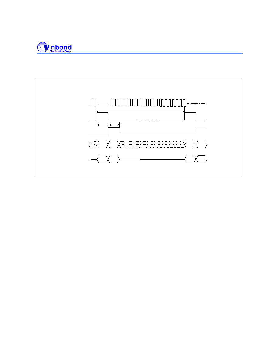
W6691
- 84 -
9.4 Preliminary Switching Characteristics
9.4.1 PCM Interface Timing
PBCK
(1.536MHz)
PFCK1
PFCK2
PTXD
PRXD
24 CHs
CH 1
CH 2
Port1
Port1
Port2
Port2
Port1
Port1
Port2
Port2
9.4.1 PCM Interface Timing
Notes:
1. These drawings are not to scale.
2. The frequency of PBCK is 1536 KHz which includes 24 channels of 64 kbps data. The PFCK1 and PFCK2 are located at
channel 1 and channel 2, each with a 8 x PBCK duration.

W6691
Publication Release Date: June 11, 2003
- 85 -
Revision 1.5
9.4.2 Detailed PCM Tming
PBCK
PFCK1
PFCK2
PTXD
PRXD
ta1
ta2
ta3
ta4
ta5
ta6
ta7
ta8
PARAMETER PARAMETER
DESCRIPTIONS MIN. NOMINAL MAX. REMARKS
ta1
PBCK pulse high
325
Unit = nS
ta2
PBCK pulse low
195
325
455
ta3
Frame clock asserted from
PBCK
20
ta4
PTXD data delay from PBCK
20
ta5
Frame clock deasserted from
PBCK
20
ta6
PTXD hold time from PBCK
10
ta7
PRXD setup time to PBCK
20
ta8
PRXD hold time from PBCK
10
Note:
The PCM clocks are locked to the S/T receive clock. At every two or three PCM frame time (125
�S), PBCK and PFCK1,
PFCK2 may be adjusted by one local oscillator cycle (130 nS) in order to synchronize with S/T clock. This shift is made on the
LOW level time of PBCK and the HIGH level time is not affected. This introduces jitters on the PBCK, PFCK1 and PFCK2 with
jitter amplitude 260 ns (peak-to-peak) and jitter frequency about 2.67~4 KHz.
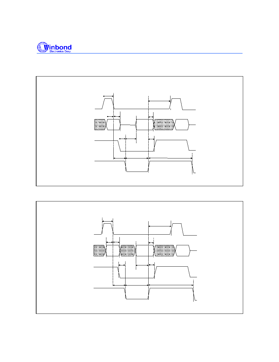
W6691
- 86 -
9.4.3 8-bit Microprocessor Timing
Intel Mode Read Cycle Timing
t1
ALE
t3
t11
t5
t10
AD<7:0>
RD#
CS#
t8
t2
A<7:0>
D<7:0>
A<7:0>
t4
t9
t6
t7
Intel Mode Write Cycle Timing
t1
ALE
t3
t13
t12
t10
AD<7:0>
WR#
CS#
t14
t2
A<7:0>
D<7:0>
A<7:0>
t4
t15
t6
t7

W6691
Publication Release Date: June 11, 2003
- 87 -
Revision 1.5
Motorola Mode Read Cycle Timing
A<7:0>
t21
CS#
RW
DS#
t19
t16
t18
t24
t20
t23
D<7:0>
t22
t17
Motorola Mode Write Cycle Timing
A<7:0>
t27
CS#
RW
DS#
t19
t16
t18
t29
t26
t28
D<7:0>
t25
t17

W6691
- 88 -
PARAMETER PARAMETER
DESCRIPTIONS MIN. MAX.
REMARKS
t1
ALE pulse width
50
t2
Address setup time to ALE
15
t3
Address hold time from ALE
10
t4
Address setup time to RD#, WR#
0
t5
RD# pulse width
110
t6
CS# setup time to RD#, WR#
0
t7
CS# hold time from RD#, WR#
0
t8
Data output delay from RD#
50
t9
Data float from RD#
25
t10
ALE guard time
15
t11
RD# recovery time
70
t12
WR# pulse width
60
t13
WR# recovery time
70
t14
Data setup time to WR#
35
t15
Data hold time from WR#
10
t16
Address setup time to DS#
25
t17
Address hold time from DS#
10
t18
CS# setup time to DS#
10
t19
CS# hold time from DS#
10
t20
DS# read pulse width
110
t21
DS# read recovery time
70
t22
RW setup time to DS# read
0
t23
Data output delay from DS#
110
t24
Data hold time from DS#
25
t25
RW setup time to DS# write
0
t26
DS# write pulse width
60
t27
DS# write recovery time
70
t28
Write data setup time to DS#
35
t29
Write data hold time from DS#
10
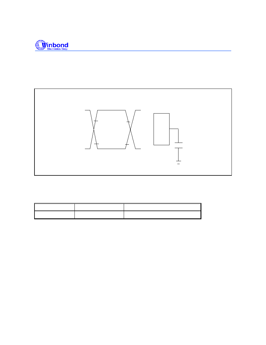
W6691
Publication Release Date: June 11, 2003
- 89 -
Revision 1.5
9.5 AC Timing Test Conditions
T
A
= 0 to 70
�C, V
DD
= 3.3V
�5%
Inputs are driven to 2.4 V for logical 1 and 0.4 V for logical 0. Measurements are made at 2.0 V for
logical 1 and 0.8 V for logical 0. The AC testing input/output waveforms are shown below:
Test Point
2.0
0.8
2.0
0.8
2.4
0.4
Device Under
Test
C
load
= 150pF
10. ORDERING INFORMATION
PART NUMBER
PACKAGE TYPE
PRODUCTION FLOW
W6691 64-pin
LQFP Commercial, 0
�C to +70 �C
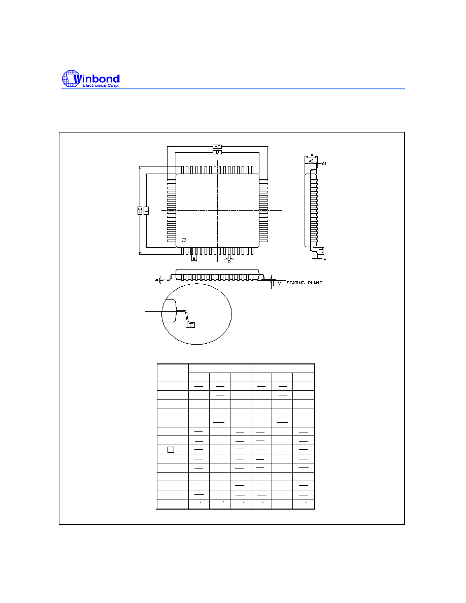
W6691
- 90 -
64L LQFP (10 x 10 x 1.4 mm)
11. PACKAGE DIMENSIONS
0
7
0
1.00
0.75
0.60
12.00
0.45
0.039
0.030
0.024
0.472
0.018
0.50
0.20
0.27
1.45
1.60
10.00
1.40
0.09
0.17
1.35
0.05
0.008
0.011
0.057
0.063
0.393
0.055
0.020
0.004
0.007
0.053
0.002
Symbol
Min. Nom. Max.
Max.
Nom.
Min.
Dimension in inch
Dimension in mm
A
b
c
D
e
H
D
H
E
L
y
A
A
L
1
1
2
E
0.008
0.20
7
0.393
10.00
0.472
12.00
0.006
0.15
0.003
0.08
3.5
3.5

W6691
Publication Release Date: June 11, 2003
- 91 -
Revision 1.5
Headquarters
No. 4, Creation Rd. III,
Science-Based Industrial Park,
Hsinchu, Taiwan
TEL: 886-3-5770066
FAX: 886-3-5665577
http://www.winbond.com.tw/
Taipei Office
TEL: 886-2-8177-7168
FAX: 886-2-8751-3579
Winbond Electronics Corporation America
2727 North First Street, San Jose,
CA 95134, U.S.A.
TEL: 1-408-9436666
FAX: 1-408-5441798
Winbond Electronics (H.K.) Ltd.
No. 378 Kwun Tong Rd.,
Kowloon, Hong Kong
FAX: 852-27552064
Unit 9-15, 22F, Millennium City,
TEL: 852-27513100
Please note that all data and specifications are subject to change without notice.
All the trade marks of products and companies mentioned in this data sheet belong to their respective owners.
Winbond Electronics (Shanghai) Ltd.
200336 China
FAX: 86-21-62365998
27F, 2299 Yan An W. Rd. Shanghai,
TEL: 86-21-62365999
Winbond Electronics Corporation Japan
Shinyokohama Kohoku-ku,
Yokohama, 222-0033
FAX: 81-45-4781800
7F Daini-ueno BLDG, 3-7-18
TEL: 81-45-4781881
9F, No.480, Rueiguang Rd.,
Neihu District, Taipei, 114,
Taiwan, R.O.C.