Document Outline
- Main Menu
- ISDN Products
- Search
- Web

Preliminary Data Sheet
W6692 PCI ISDN S/T-Controller
Publication Release Date: Sep 30, 1999
Revision 0.9
-1 -
W6692
PCI Bus ISDN S/T-Controller
Data Sheet

Preliminary Data Sheet
W6692 PCI ISDN S/T-Controller
Publication Release Date: Sep 30, 1999
Revision 0.9
-2 -
The information described in this document is the exclusive intellectual property of Winbond
Electronics Corp and shall not be reproduced without permission from Winbond.
Winbond is providing this document only for reference purposes for W6692-based system design.
Winbond assumes no responsibility for errors or omissions. All data and specifications are subject to
change without notice.

Preliminary Data Sheet
W6692 PCI ISDN S/T-Controller
Publication Release Date: Sep 30, 1999
Revision 0.9
-3 -
TABLE OF CONTENTS
1. GENERAL DESCRIPTION
..........................................................................................................9
2. FEATURES
...................................................................................................................................9
3. PIN CONFIGURATION
............................................................................................................10
4. PIN DESCRIPTION
...................................................................................................................13
5
. SYSTEM DIAGRAM AND APPLICATIONS
...........................................................................16
6. BLOCK DIAGRAM
....................................................................................................................17
7. FUNCTIONAL DESCRIPTIONS
...............................................................................................18
7.1 Main Block Functions......................................................................................................................................................18
7.2 Layer 1 Functions Descriptions.......................................................................................................................................19
7.2.1 S/T Interface Transmitter/Receiver .............................................................................................................................19
7.2.2 Receiver Clock Recovery And Timing Generation ......................................................................................................24
7.2.3 Layer 1 Activation/Deactivation..................................................................................................................................24
7.2.3.1 States Descriptions And Command/Indication Codes ...........................................................................................24
7.2.3.2 State Transition Diagrams....................................................................................................................................26
7.2.4 D Channel Access Control ..........................................................................................................................................30
7.2.5 Frame Alignment........................................................................................................................................................30
7.2.5.1 FAinfA_1fr ..........................................................................................................................................................31
7.2.5.2 FAinfB_1fr ..........................................................................................................................................................31
7.2.5.3 FAinfD_1fr ..........................................................................................................................................................32
7.2.5.4 FAinfA_kfr ..........................................................................................................................................................32
7.2.5.5 FAinfB_kfr ..........................................................................................................................................................33
7.2.5.6 FAinfD_kfr ..........................................................................................................................................................33
7.2.5.7 Faregain...............................................................................................................................................................34
7.2.6 Multiframe Synchronization .......................................................................................................................................34
7.2.7 Test Functions ............................................................................................................................................................36
7.3 Serial Interface Bus .........................................................................................................................................................38
7.4 B Channel Switching .......................................................................................................................................................38
7.5 PCM Port .........................................................................................................................................................................40
7.6 D Channel HDLC Controller ..........................................................................................................................................40
7.6.1 D Channel Message Transfer Modes...........................................................................................................................41

Preliminary Data Sheet
W6692 PCI ISDN S/T-Controller
Publication Release Date: Sep 30, 1999
Revision 0.9
-4 -
7.6.2 Reception of Frames in D Channel..............................................................................................................................41
7.6.3 Transmission of Frames in D Channel ........................................................................................................................42
7.7 B Channel HDLC Controller ..........................................................................................................................................43
7.7.1 Reception of Frames in B Channel
.........................................................................................................................43
7.7.2 Transmission of Frames in B Channel ........................................................................................................................44
7.8 GCI Mode Serial Interface Bus.......................................................................................................................................45
7.8.1 GCI Mode C/I0 Channel Handling..............................................................................................................................46
7.8.2 GCI Mode Monitor Channel Handling........................................................................................................................46
7.9 PCI/MP Interface Circuit................................................................................................................................................48
7.9.1 PCI Slave Mode And Configuration Serial EEPROM .................................................................................................48
7.9.2 8-bit Microprocessor Interface.....................................................................................................................................49
7.10 Peripheral Control.........................................................................................................................................................49
8. REGISTER DESCRIPTIONS ......................................................................................................51
8.1 Chip Control and D_ch HDLC controller ......................................................................................................................51
8.1.1 D_ch receive FIFO
D_RFIFO Read Address 00H/00H ...........................................................................................53
8.1.2 D_ch transmit FIFO
D_XFIFO Write Address 04H/01H.........................................................................................53
8.1.3 D_ch command register
D_CMDR Read/Write Address 08H/02H ...........................................................................54
8.1.4 D_ch Mode Register
D_MODE Read/Write Address 0CH/03H................................................................................54
8.1.5 Timer 1 Register
TIMR1 Read/Write Address 10H/04H ........................................................................................55
8.1.6 Interrupt Status Register
ISTA Read_clear Address 14H/05H.............................................................................56
8.1.7 Interrupt Mask Register
IMASK R/W Address 18H/06H..........................................................................................57
8.1.8 D_ch Extended Interrupt Register
D_EXIR Read_clear Address 1CH ......................................................................57
8.1.9 D_ch Extended Interrupt Mask Register
D_EXIM Read/Write Address 20H/08H ....................................................58
8.1.10 D_ch Status Register
D_XSTA Read Address 24H/09H .....................................................................................58
8.1.11 D_ch Receive Status Register
D_RSTA Read Address 28H/0AH .........................................................................59
8.1.12 D_ch SAPI Address Mask
D_SAM Read/Write Address 2CH/0BH......................................................................59
8.1.13 D_ch SAPI1 Register
D_SAP1 Read/Write Address 30H/0CH .............................................................................60
8.1.14 D_ch SAPI2 Register
D_SAP2 Read/Write Address 34H/0DH...............................................................................60
8.1.15 D_ch TEI Address Mask
D_TAM Read/Write Address 38H/0EH .........................................................................60
8.1.16 D_ch TEI1 Register
D_TEI1 Read/Write Address 3CH/0FH................................................................................61
8.1.17 D_ch TEI2 Register
D_TEI2 Read/Write Address 40H/10H ................................................................................61
8.1.18 D_ch Receive Frame Byte Count High
D_RBCH Read Address 44H/11H............................................................61
8.1.19 D_ch Receive Frame Byte Count Low
D_RBCL Read Address 48H/12H.............................................................62
8.1.20 Timer 2
TIMR2 Write Address 4CH/13H..........................................................................................62
8.1.21 Layer 1_Ready Code
L1_RC Read/Write Address 50H/14H ...............................................................62
8.1.22 Control Register
CTL Read/Write Address 54H/15H .............................................................................................63
8.1.23 Command/Indication Receive Register
CIR Read Address 58H/16H ....................................................................63
8.1.24 Command/Indication Transmit Register
CIX Read/Write Address 5CH/17H........................................................64
8.1.25 S/Q Channel Receive Register
SQR Read Address 60H/18H..............................................................................64
8.1.26 S/Q Channel Transmit Register
SQX Read/Write Address 64H/19H ..................................................................65
8.1.27 Peripheral Control Register
PCTL Read/Write Address 68H/1AH ....................................................................65
8.1.28 Monitor Receive Channel 0
MO0R Read Address 6CH/1BH ............................................................................66
8.1.29 Monitor Transmit Channel 0
MO0X Read/Write Address 70H/1CH .................................................................67
8.1.30 Monitor Channel 0 Interrupt Register
MO0I Read_clear Address 74H/1DH......................................................67
8.1.31 Monitor Channel 0 Control Register
MO0C Read/Write Address 78H/1EH..........................................................67

Preliminary Data Sheet
W6692 PCI ISDN S/T-Controller
Publication Release Date: Sep 30, 1999
Revision 0.9
-5 -
8.1.32 GCI Mode Control/Status Register
GCR Read/Write Address 7CH/1FH.......................................68
8.1.33 Peripheral Address Register
XADDR Read/Write Address F4H/3DH ...............................................................69
8.1.34 Peripheral Data Register
XDATA Read/Write Address F8H/3EH.....................................................................70
8.1.35 Serial EEPROM Control Register
EPCTL Read/Write Address FCH/3FH ............................................................71
8.1.36 Monitor Receive Channel 1 Register
MO1R Read Address 6DH/40H .................................................................71
8.1.37 Monitor Transmit Channel 1
MO1X Read/Write Address 71H/41H..................................................................72
8.1.38 Monitor Channel 1 Interrupt Register
MO1I Read_clear Address 75H/42H ......................................................72
8.1.39 Monitor Channel 1 Control Register
MO1C Read/Write Address 79H/43H ..........................................................72
8.1.40 GCI IC1 Receive Register
IC1R Read Address 6EH/44H................................................................................73
8.1.41 GCI IC1 Transmit Register
IC1X Read/Write Address 72H/45H.....................................................................73
8.1.42 GCI IC2 Receive Register
IC2R Read Address 6FH/46H ................................................................................73
8.1.43 GCI IC2 Transmit Register
IC2X Read/Write Address 73H/47H.....................................................................73
8.1.44 GCI CI1 Indication Register
CI1R Read Address 7DH/48H ............................................................................74
8.1.45 GCI CI1 Command Register
CI1X Read/Write Address 7EH/49H ..................................................................74
8.1.46 GCI Extended Interrupt Register
GCI_EXIR Read_clear Address 76H/4AH ..........................................................74
8.1.47 GCI Extended Interrupt Mask Register
GCI_EXIM Read/Write Address 7AH/4BH ...............................................75
8.2 B1 HDLC controler .........................................................................................................................................................75
8.2.1 B1_ch receive FIFO
B1_RFIFO Read Address 80H/20H .....................................................................................76
8.2.2 B1_ch transmit FIFO
B1_XFIFO Write Address 84H/21H .................................................................................76
8.2.3 B1_ch command register
B1_CMDR Read/Write Address 88H/22H....................................................................77
8.2.4 B1_ch Mode Register
B1_MODE Read/Write Address 8CH/23H ..........................................................................78
8.2.5 B1_ch Extended Interrupt Register
B1_EXIR Read_clear Address 90H/24H ............................................................79
8.2.6 B1_ch Extended Interrupt Mask Register
B1_EXIM Read/Write Address 94H/25H .................................................80
8.2.7 B1_ch Status Register
B1_STAR Read Address 98H/26H......................................................................................80
8.2.8 B1_ch Address Mask Register 1
B1_ADM1 Read/Write Address 9CH/27H...........................................................81
8.2.9 B1_ch Address Mask Register 2
B1_ADM2 Read/Write Address A0H/28H...........................................................81
8.2.10 B1_ch Address Register 1
B1_ADR1 Read/Write Address A4H/29H ...................................................................81
8.2.11 B1_ch Address Register 2
B1_ADR2 Read/Write Address A8H/2AH ..................................................................82
8.2.12 B1_ch Receive Frame Byte Count Low
B1_RBCL Read Address ACH/2BH..........................................................82
8.2.13 B1_ch Receive Frame Byte Count High
B1_RBCH Read Address B0H/2CH .........................................................82
8.2.14 B1_ch Transmit Idle Pattern
B1_IDLE Read/Write Address B4H/2DH ..................................................................83
8.3 B2 HDLC controller ........................................................................................................................................................83
8.4 PCI Configuration Register.............................................................................................................................................84
8.4.1 Device/Vendor ID Register
Read Address 00
H
.................................................................................................85
8.4.2 Status/Command Register
Read/Write Address 04
H
...........................................................................................85
8.4.3 Class Code/Revision ID Register
Read Address 08
H
..........................................................................................87
8.4.4 Header Type/Latency Timer Register
Read Address 0C
H
....................................................................................87
8.4.5 Base Address Register 0
Read/Write Address 10
H
............................................................................................88
8.4.6 Base Address Register 1
Read/Write Address 14
H
.............................................................................................89
8.4.7 Subsystem/Subsystem Vendor ID Register
Read Address 2C
H
...........................................................................89
8.4.8 Interrupt Line Register
Read/Write Address 3C
H
...............................................................................................90
8.4.9 Capability Pointer
Read Address 34
H
................................................................................................................90
8.4.10 Power Management Capability
Read Address 40
H
...........................................................................................91
8.4.11 Power Management Control/Status
Read/Write Address 44
H
...........................................................................92
9. ELECTRICAL CHARACTERISTICS...........................................................................................94
9.1 Absolute Maximum Rating..............................................................................................................................................94

Preliminary Data Sheet
W6692 PCI ISDN S/T-Controller
Publication Release Date: Sep 30, 1999
Revision 0.9
-6 -
9.2 Power Supply ...................................................................................................................................................................94
9.3 DC Characteristics ..........................................................................................................................................................94
9.4 Preliminary Switching Characteristics ...........................................................................................................................96
9.4.1 PCM Interface Timing
1)
..............................................................................................................................................96
9.4.2 Serial EEPROM Timing .............................................................................................................................................97
9.4.3 Peripheral Interface Timing ........................................................................................................................................97
9.4.5 8-bit Microprocessor Timing.......................................................................................................................................98
9.5 AC Timing Test Conditions...........................................................................................................................................101
10. PACKAGE SPECIFICATIONS ................................................................................................102

Preliminary Data Sheet
W6692 PCI ISDN S/T-Controller
Publication Release Date: Sep 30, 1999
Revision 0.9
-7 -
LIST OF FIGURES
FIG.3.1 W6692 PIN CONFIGURATION - PCI MODE ..........................................................................................................10
FIG.3.2 W6692 PIN CONFIGURATION - INTEL BUS MODE ............................................................................................11
FIG.3.3 W6692 PIN CONFIGURATION - MOTOROLA BUS MODE .................................................................................12
FIG.5.1 ISDN INTERNET PASSIVE S-CARD WITH TWO POTS CONNECTIONS .........................................................16
FIG.6.1 W6692 FUNCTIONAL BLOCK DIAGRAM .............................................................................................................17
FIG.7.1 FRAME STRUCTURE AT S/T INTERFACE ...........................................................................................................20
FIG.7.2 W6692 WIRING CONFIGURATION IN TE APPLICATIONS ...............................................................................21
FIG.7.3 EXTERNAL TRANSMITTER CIRCUITRY ............................................................................................................22
FIG.7.4 EXTERNAL RECEIVER CIRCUITRY.....................................................................................................................22
FIG.7.5 LAYER 1 ACTIVATION/DEACTIVATION STATE DIAGRAM - NORMAL MODE..........................................28
FIG.7.6 LAYER 1 ACTIVATION/DEACTIVATION STATE DIAGRAM - SPECIAL MODE...........................................29
FIG.7.7 SSP AND SCP TEST SIGNALS..................................................................................................................................37
FIG 7.8 GCI MODE CHANNEL STRUCTURE .....................................................................................................................46
FIG.7.9 SERIAL EEPROM DATA LAYOUT.........................................................................................................................48

Preliminary Data Sheet
W6692 PCI ISDN S/T-Controller
Publication Release Date: Sep 30, 1999
Revision 0.9
-8 -
LIST OF TABLES
TABLE 4.1 W6692 PIN DESCRIPTIONS ...........................................................................................................................13
TABLE 7.1 OUTPUT PHASE DELAY COMPENSATION TABLE .................................................................................24
TABLE 7.2 LAYER 1 COMMAND CODES .......................................................................................................................26
TABLE 7.3 LAYER 1 INDICATION CODES.....................................................................................................................26
TABLE 7.4 D PRIORITY CLASSES ...................................................................................................................................30
TABLE 7.5 D PRIORITY COMMANDS/INDICATIONS ..................................................................................................30
TABLE 7.6 MULTIFRAME STRUCTURE IN S/T INTERFACE .....................................................................................35
TABLE 8.1 REGISTER ADDRESS MAP : CHIP CONTROL AND D CHANNEL HDLC..............................................51
TABLE 8.2 REGISTER SUMMARY : CHIP CONTROL AND D CHANNEL HDLC ..................................................52
TABLE 8.3 REGISTER ADDRESS MAP : B1 CHANNEL HDLC ....................................................................................75
TABLE 8.4 REGISTER SUMMARY : B1 CHANNEL HDLC...........................................................................................76
TABLE 8.5 REGISTER ADDRESS MAP : B2 CHANNEL HDLC ....................................................................................83
TABLE 8.6 REGISTER SUMMARY : B2 CHANNEL HDLC...........................................................................................83
TABLE 8.7 PCI CONFIGURATION SPACE ...................................................................................................................84

Preliminary Data Sheet
W6692 PCI ISDN S/T-Controller
Publication Release Date: Sep 30, 1999
Revision 0.9
-9 -
1. GENERAL DESCRIPTION
The Winbond
'
s single chip PCI bus ISDN S/T interface controller (W6692) is an all-in-one device suitable for ISDN Internet
access. Three HDLC controllers are incorporated in the chip, one for D channel and the other two for B channels. These HDLC
controllers facilitate efficient access to signaling and data services. The PCM codec interface provides voice service or other
services. The built in PCI 2.2 interface circuit makes glueless design for PCI bus add-on card application.
2. FEATURES
* Full duplex 2B + D S/T-interface transceiver compliant with ITU-T I.430 Recommendation
* One D channel HDLC controller
- Maskable address recognition
- Transparent (HDLC) mode
- FIFO buffer (2 x 128 bytes)
* Two B channel HDLC controllers
- Maskable address recognition
- Bit rate options : 56 or 64 kbps
- Transparent (HDLC mode) or extended transparent mode (clear channel)
- FIFO buffer (2 x 128 bytes) per B channel
* Two PCM codec interfaces for speech and POTS application
* Various B channel switching capabilities
* GCI master/slave interface
* Built in PCI 2.2 slave mode circuit
* ACPI capability : PCI 2.2 and PCI Power Management 1.1 compliant
* Serial EEPROM interface for PCI configuration
* Peripheral control pins
* 8-bit microprocessor interface when PCI is disabled for TA application
* Digital : 5V or 3.3V, analog : 5V
* Advanced CMOS technology
* Low power consumption
* 100-pin QFP package

Preliminary Data Sheet
W6692 PCI ISDN S/T-Controller
Publication Release Date: Sep 30, 1999
Revision 0.9
-10 -
3. PIN CONFIGURATION
W6692
ISDN-PCI
1 2 3
7
4 5 6
1
1
8 9
1
0
1
3
1
2
1
7
1
4
1
5
1
6
1
8
1
9
2
0
2
1
2
2
2
3
2
4
2
5
2
6
2
7
2
8
2
9
3
0
5
8
31
32
33
34
35
36
37
38
39
40
41
42
43
44
45
46
47
48
49
50
5
1
5
2
5
3
5
4
5
5
5
6
5
7
6
0
5
9
6
1
8
0
6
2
6
3
6
4
6
5
6
6
6
7
6
8
6
9
7
0
7
1
7
2
7
3
7
4
7
5
7
6
7
7
7
8
7
9
81
88
82
83
84
85
86
87
89
100
90
91
92
93
94
95
96
97
98
99
I
O
3
/
X
A
D
3
P
E
R
R
#
X
T
A
L
2
I
O
6
/
X
A
D
6
C
/
B
E
1
#
P
A
R
D
E
V
S
E
L
#
V
D
D
D
F
R
A
M
E
#
T
O
U
T
2
V
D
D
D
S
T
O
P
#
V
S
S
D
T
R
D
Y
#
I
R
D
Y
#
A
D
1
7
C
/
B
E
2
#
A
D
1
6
A
D
1
8
A
D
1
9
V
D
D
B
V
S
S
B
AD29
AD24
AD25
AD26
CLK
AD27
AD28
VDDB
AD30
VSSB
AD31
VDDD
VSSD
VSSB
AD9
AD8
C/BE0#
AD7
AD6
VSSB
AD5
VDDB
AD3
AD2
AD4
P
M
E
#
V
D
D
D
V
S
S
D
X
T
A
L
1
P
F
C
K
1
P
B
C
K
T
E
S
T
P
P
F
C
K
2
AD0
AD1
I
O
8
/
X
A
L
E
P
T
X
D
D
D
D
U
V
S
S
D
S
X
1
S
X
2
P
R
X
D
V
A
U
X
/
V
D
D
A
X
I
N
T
I
N
1
X
I
N
T
I
N
0
RST#
F
S
C
E
P
S
D
I
E
P
S
D
O
AD10
AD11
VDDB
A
D
1
3
A
D
1
4
I
O
2
/
X
A
D
2
I
O
1
/
X
A
D
1
I
O
0
/
X
A
D
0
I
O
4
/
X
A
D
4
I
O
5
/
X
A
D
5
I
O
7
/
X
A
D
7
A
D
1
2
A
D
1
5
SR1
VSSA
SR2
E
P
C
S
D
C
L
E
P
S
K
I
O
9
/
X
R
D
B
I
O
1
0
/
X
W
R
B
I
N
T
A
#
C/BE3#
IDSEL
AD23
AD22
AD21
AD20
FIG.3.1 W6692 PIN CONFIGURATION - PCI MODE

Preliminary Data Sheet
W6692 PCI ISDN S/T-Controller
Publication Release Date: Sep 30, 1999
Revision 0.9
-11 -
W6692
ISDN-PCI
1 2 3
7
4 5 6
1
1
8 9
1
0
1
3
1
2
1
7
1
4
1
5
1
6
1
8
1
9
2
0
2
1
2
2
2
3
2
4
2
5
2
6
2
7
2
8
2
9
3
0
5
8
31
32
33
34
35
36
37
38
39
40
41
42
43
44
45
46
47
48
49
50
5
1
5
2
5
3
5
4
5
5
5
6
5
7
6
0
5
9
6
1
8
0
6
2
6
3
6
4
6
5
6
6
6
7
6
8
6
9
7
0
7
1
7
2
7
3
7
4
7
5
7
6
7
7
7
8
7
9
81
88
82
83
84
85
86
87
89
100
90
91
92
93
94
95
96
97
98
99
I
O
3
/
X
A
D
3
X
T
A
L
2
I
O
6
/
X
A
D
6
W
R
#
V
D
D
D
C
S
#
T
O
U
T
2
V
D
D
D
V
S
S
D
V
D
D
B
V
S
S
B
CLK
VDDB
VSSB
VDDD
VSSD
VSSB
RD#
AD7
AD6
VSSB
AD5
VDDB
AD3
AD2
AD4
V
D
D
D
V
S
S
D
X
T
A
L
1
P
F
C
K
1
P
B
C
K
T
E
S
T
P
P
F
C
K
2
AD0
AD1
I
O
8
/
X
A
L
E
P
T
X
D
D
D
D
U
V
S
S
D
S
X
1
S
X
2
P
R
X
D
V
D
D
A
X
I
N
T
I
N
1
X
I
N
T
I
N
0
RST#
F
S
C
VDDB
I
O
2
/
X
A
D
2
I
O
1
/
X
A
D
1
I
O
0
/
X
A
D
0
I
O
4
/
X
A
D
4
I
O
5
/
X
A
D
5
I
O
7
/
X
A
D
7
SR1
VSSA
SR2
D
C
L
I
O
9
/
X
R
D
B
I
O
1
0
/
X
W
R
B
I
N
T
#
A
L
E
FIG.3.2 W6692 PIN CONFIGURATION - INTEL BUS MODE

Preliminary Data Sheet
W6692 PCI ISDN S/T-Controller
Publication Release Date: Sep 30, 1999
Revision 0.9
-12 -
W6692
ISDN-PCI
1 2 3
7
4 5 6
1
1
8 9
1
0
1
3
1
2
1
7
1
4
1
5
1
6
1
8
1
9
2
0
2
1
2
2
2
3
2
4
2
5
2
6
2
7
2
8
2
9
3
0
5
8
31
32
33
34
35
36
37
38
39
40
41
42
43
44
45
46
47
48
49
50
5
1
5
2
5
3
5
4
5
5
5
6
5
7
6
0
5
9
6
1
8
0
6
2
6
3
6
4
6
5
6
6
6
7
6
8
6
9
7
0
7
1
7
2
7
3
7
4
7
5
7
6
7
7
7
8
7
9
81
88
82
83
84
85
86
87
89
100
90
91
92
93
94
95
96
97
98
99
I
O
3
/
X
A
D
3
X
T
A
L
2
I
O
6
/
X
A
D
6
D
S
#
V
D
D
D
C
S
#
T
O
U
T
2
V
D
D
D
V
S
S
D
V
D
D
B
V
S
S
B
CLK
VDDB
VSSB
VDDD
VSSD
VSSB
RW
D7
D6
VSSB
D5
VDDB
D3
D2
D4
V
D
D
D
V
S
S
D
X
T
A
L
1
P
F
C
K
1
P
B
C
K
T
E
S
T
P
P
F
C
K
2
D0
D1
I
O
8
/
X
A
L
E
P
T
X
D
D
D
D
U
V
S
S
D
S
X
1
S
X
2
P
R
X
D
V
D
D
A
X
I
N
T
I
N
1
X
I
N
T
I
N
0
RST#
F
S
C
VDDB
I
O
2
/
X
A
D
2
I
O
1
/
X
A
D
1
I
O
0
/
X
A
D
0
I
O
4
/
X
A
D
4
I
O
5
/
X
A
D
5
I
O
7
/
X
A
D
7
SR1
VSSA
SR2
D
C
L
I
O
9
/
X
R
D
B
I
O
1
0
/
X
W
R
B
I
N
T
#
A0
A1
A2
A3
A
4
A
5
A
6
A
7
FIG.3.3 W6692 PIN CONFIGURATION - MOTOROLA BUS MODE

Preliminary Data Sheet
W6692 PCI ISDN S/T-Controller
Publication Release Date: Sep 30, 1999
Revision 0.9
-13 -
4. PIN DESCRIPTION
TABLE 4.1 W6692 PIN DESCRIPTIONS
Notation : The suffix
"
#
"
indicates an active LOW signal.
Pin
Name
Pin
Number
Type
Functions
PCI Bus
CLK
84
I
PCI Mode : PCI Clock. All other PCI signals, except RST#, INTA# are
sampled on the rising edge of CLK. According to PCI 2.1/2.2
specification, CLK is stable at least 100
�
s (Trst-clk) before deassertion
of RST#.
Intel Bus Mode : Must be pulled to HIGH.
Motorola Bus Mode : Must be pulled to LOW.
AD31-AD0
85,86,87,90,91,
92,93,94,97,98,
99,100,7,8,9,10,
23,24,25,30,33,
34,35,36,38,39,
40,41,44,45,46,
47
I/O
Address and Data are multiplexed on the same PCI pins. During the
address phase, AD31-0 contain a 32-bit physical address. During the
data phase, AD7-AD0 contain the least significant byte and AD31-
AD24 contain the most significant byte.
C/BE3#-C/BE0#
95,11,22,37
I
Bus command and Byte Enables.
During the address phase of a transaction, they define the bus
command.
During data phase, they are used as Byte Enables.
PAR
21
I/O
Parity is even parity across AD31-AD0 and C/BE3#-C/BE0#.
FRAME#
12
I
FRAME# is asserted to indicate a bus transaction is beginning.
TRDY#
14
O
Target Ready indicates W6692 is able to complete the current data
phase of the transaction.
IRDY#
13
I
Initiator Ready indicates the bus master
s ability to complete the current
data phase of the transaction.
STOP#
18
O
Stop indicates W6692 is requesting the master to stop the current
transaction.
DEVSEL#
15
O
Device Select indicates W6692 has decoded itself as the target of the
current access.
IDSEL
96
I
Initialization Device Select is used as chip select during configuration
transactions.
PERR#
19
O
Parity Error is used for reporting of data parity errors.
RST#
81
I
PCI Reset. RST# may be asynchronous to CLK when asserted or
deasserted.
INTA#
80
O
Interrupt. This is level sensitive, active LOW and open drain output.
Intel Bus Mode (Selected when CLK=HIGH)
CLK
84
I
This pin must be pulled to HIGH.
AD7-0
38,39,40,41,44,45
,46,47
I/O
Multiplexed address and data. During the address phase, AD7-0 contain
a 8-bit physical address. During the data phase, AD7-AD0 contain data.

Preliminary Data Sheet
W6692 PCI ISDN S/T-Controller
Publication Release Date: Sep 30, 1999
Revision 0.9
-14 -
CS#
12
I
Chip select.
ALE
13
I
Address Latch Enable. Used to latch addresses.
RD#
37
I
Read.
WR#
22
I
Write.
RST#
81
I
Reset.
INT#
80
O
Interrupt. This is a level sensitive, active LOW and open drain output.
Motorola Bus Mode (Selected when CLK=LOW)
CLK
84
I
This pin must be pulled to LOW.
D7-D0
38,39,40,41,44,45
,46,47
I/O
Data.
A7-A0
7,8,9,10,33,34,35,
36
I
Address.
CS#
12
I
Chip select.
DS#
22
I
Data strobe.
RW
37
I
Read/write identify. HIGH for read, and LOW for write.
RST#
81
I
Reset.
INT#
80
O
Interrupt. This is a level sensitive, active LOW and open drain output.
GCI Bus
DCL
72
I
GCI Bus Data Clock of the frequency: 1.536 MHz.
FSC
71
I
GCI Bus Frame Synchronization Clock: 8KHz.
DD
70
I/O
GCI Bus Data Downstream : Slave mode - input, master mode - output.
DU
69
I/O
GCI Bus Data Upstream : Slave mode - output, master mode - input.
PCM Interface
PFCK1
64
O
PCM port 1 frame synchronization signal, with 8 KHz repetition rate
and 8 bit pulse width.
PFCK2
62
O
PCM port 2 frame synchronization signal, with 8 KHz repetition rate
and 8 bit pulse width.
PBCK
63
O
PCM bit synchronization clock of 1.536 MHz.
PTXD
65
O
PCM transmit data output. A maximum of two channels with 64 Kbit/s
data rate can be multiplexed on this signal.
PRXD
66
I
PCM receive data input. A maximum of two channels with 64 Kbit/s
data rate can be multiplexed on this signal.
ISDN Signals and External Crystal
SR1
49
I
S/T bus receiver input (negative).
SR2
50
I
S/T bus receiver input (positive).
SX1
54
O
S/T bus transmitter output (positive).
SX2
55
O
S/T bus transmitter output (negative).
XTAL1
56
I
Crystal or Oscillator clock input. The clock frequency:
7.68MHz
�
100PPM.
XTAL2
57
O
Crystal clock output. Left unconnected when using oscillator.
External EEPROM Interface
EPCS
73
O
Serial EEPROM chip select (active HIGH).
EPSK
74
O
Serial EEPROM data clock (clock frequency < 250 KHz).
EPSDI
76
I
Serial EEPROM data input.
EPSDO
75
O
Serial EEPROM data output.
Functional Test
TESTP
61
I
Used to enable normal operation (1) or enter test mode (0).
PCI Power Management

Preliminary Data Sheet
W6692 PCI ISDN S/T-Controller
Publication Release Date: Sep 30, 1999
Revision 0.9
-15 -
PME
60
O
Power Management Event Signal. Level triggered, active HIGH. Drive
a transistor to PME# in PCI slot.
Peripheral Control
TOUT2
20
O
Timer 2 output. A square wave with 50 % duty cycle, 1~63 ms period
can be generated.
XINTIN0
52
I
A level change (either direction) will generate a maskable interrupt on
the PCI bus interrupt request pin INTA#.
XINTIN1
53
I
A level change (either direction) will generate a maskable interrupt on
the PCI bus interrupt request pin INTA#.
IO0-IO10
79,78,77,29,28,
27,26,4,3,2,1
I/O
When confiured as simple IO mode (PCTL:XMODE = 0), these pins
can read/write data from/to peripheral components. The pin directions
are selected via register.
XAD7-XAD0
29,28,27,26,
4,3,2,1
I/O
When configured as microprocessor mode (PCTL:XMODE = 1),
address and data are multiplexed on these pins.
XALE
77
O
When configured as microprocessor mode (PCTL:XMODE = 1), this is
the Address Latch Enable output.
XRDB
78
O
When configured as microprocessor mode (PCTL:XMODE = 1), this is
the read pulse.
XWRB
79
O
When configured as microprocessor mode (PCTL:XMODE = 1), this is
the write pulse.
Power and Ground
VDDD
17,58,67,83
I
Digital Power Supply (5V
�
5%).
VDDA
51
I
Analog Power Supply (5V
�
5%).
VDDB
6,32,43,89
I
PCI Bus Power Supply.
VSSD
16,59,68,82
I
Digital Ground.
VSSA
48
I
Analog Ground.
VSSB
5,31,42,88
I
PCI Bus Ground.
Preliminary Data Sheet
W6692 PCI ISDN S/T-Controller
Publication Release Date: Sep 30, 1999
Revision 0.9
-16 -
5
. SYSTEM DIAGRAM AND APPLICATIONS
Typical applications include :
- PCI passive S-card for data only service
- PCI passive S-card with one handset/POTS connection
- PCI passive S-card with two POTS connections
- ISDN TA or other embedded application
The all-in-one characteristic of W6692 makes it excellent for passive ISDN PCI card. W6692 integrates three HDLC
controllers in the chip and interfaces to PCI bus directly. In addition, W6692 provides peripheral control circuits for PCM
CODEC and POTS interface.
In the following application, only a few TTL-like glue circuits are needed for the two POTS interface control.
W6692 also integrates the 8-bit Intel or Motorola microprocessor interface which makes it excellent for TA application.
Transformer
Module
W6692
PCI
S-Controller
PCM
Codec
x2
4-wire S/T
EEPROM
POTS
Circuit
x2
Protection
Circuit
NT
Phone
Fax
FIG.5.1 ISDN INTERNET PASSIVE S-CARD WITH TWO POTS CONNECTIONS
Preliminary Data Sheet
W6692 PCI ISDN S/T-Controller
Publication Release Date: Sep 30, 1999
Revision 0.9
-17 -
6. BLOCK DIAGRAM
The block diagram of W6692 is shown in Figure 6.1
B-channel Switching
PCI Bus/Microprocessor
D
B1
B2
Line
Transceiver
&
AMI/BIN
Conversion
GCI
Circuit
4-wire S/T
2B+D
Serial
Interface
Bus
(SIB)
2B+D
D
HDLC
Controller
B1
HDLC
Controller
B2
HDLC
Controller
FIFO
FIFO
FIFO
PCM
Port
PCM CODEC
PCI/MP Interface Circuit
GCI Bus
DPLL and Timing Generator
Crystal/Oscillator
(7.68 MHz)
Peripheral Control
POTS
circuit
Serial
EEPROM
Interface
Serial
EEPROM
FIG.6.1 W6692 FUNCTIONAL BLOCK DIAGRAM

Preliminary Data Sheet
W6692 PCI ISDN S/T-Controller
Publication Release Date: Sep 30, 1999
Revision 0.9
-18 -
7. FUNCTIONAL DESCRIPTIONS
7.1 Main Block Functions
The functional block diagram of W6692 is shown in Fig.6.1. The main function blocks are :
- Layer 1 function according to ITU-T I.430
- Serial Interface Bus (SIB)
- B channel switching
- GCI bus interface
- PCM port and internal switching (x 2)
- D channel HDLC controller
- B channel HDLC controllers (x 2)
- PCI/microprocessor interface circuit
- Serial EEPROM interface for PCI Configuration purpose
- Peripheral control
The layer 1 function includes:
- S/T bus transmitter/receiver
- Timing recovery using Digital Phase Locked Loop (DPLL) circuit
- Layer 1 activation/deactivation
- D channel access control
- Frame alignment
- Multi-frame synchronization
- Test functions
The serial interface bus performs the multiplexing/demultiplexing of D and 2B channels.
The B channel switching determines the connection between layer1/GCI, layer 2 and PCM.
The GCI circuit is used to connect a U transceiver (slave mode) or other slave GCI device (master mode).
The PCM port provides two 64 kbps clear channels to connect to PCM codec chips and switching between two PCM ports.
The D channel HDLC controller performs the LAPD (Link Access Procedure on the D channel) protocol according to ITU-T
I.441/Q.921 recommendation.
There are two independent B channel HDLC controllers. They can be used to support HDLC-like protocols such as Internet PPP.
Two B channels are also handled by one HDLC controller to support OCN application.
The PCI interface circuit implements PCI specification revision 2.2 slave mode function. When PCI circuit is disabled, a 8-bit
microprocessor interface is used to control the chip.

Preliminary Data Sheet
W6692 PCI ISDN S/T-Controller
Publication Release Date: Sep 30, 1999
Revision 0.9
-19 -
The peripheral control block is used to control other peripheral devices such as CODEC, SLIC, DTMF detector, LEDs.
7.2 Layer 1 Functions Descriptions
The layer 1 functions includes :
- Transmitter/Receiver which conform to the electrical specifications of ITU-T I.430
- Receiver clock recovery and timing generation
- Output phase delay (deviation) compensation
- Layer 1 activation/deactivation procedures
- D channel access control
- Frame alignment
- Multi-frame synchronization
- Test functions
7.2.1 S/T Interface Transmitter/Receiver
According to ITU-T I.430, pseudo-ternary code with 100% pulse width is used in both directions of transmission on the S/T
interface. The binary "1" is represented by no line signal (zero volt), whereas a binary "0" is represented by a positive or negative
pulse.
Data transmissions on the S/T interface are arranged as frame structures. The frame is 250
�
s long and consists of 48 bits,
which corresponds to a 192 kbit/s line rate. Each frame carries two octets of B1 channel, two octets of B2 channel and four D
channel bits. Therefore, the 2B+D data rate is 144 kbit/s. The frame structure is shown in Fig.7.1.
The frame begin is marked by a framing bit, which is followed by a DC balancing bit. The first binary "0" following the
framing bit balancing bit is of the same polarity as the framing bit balancing bit, and subsequent binary zeros must alternate in
polarity.

Preliminary Data Sheet
W6692 PCI ISDN S/T-Controller
Publication Release Date: Sep 30, 1999
Revision 0.9
-20 -
FIG.7.1 FRAME STRUCTURE AT S/T INTERFACE
There are three wiring configurations according to I.430 : point-to-point, short passive bus and extended pass bus. They are
shown in Fig.7.2.
D L F L B
1
B
1
B
1
B
1
B
1
B
1
B
1
B
1
E D A F
A
N B
2
B
2
B
2
B
2
B
2
B
2
B
2
B
2
E D MB
1
B
1
B
1
B
1
B
1
B
1
B
1
B
1
E D S B
2
B
2
B
2
B
2
B
2
B
2
B
2
B
2
E D
L F L
0
1
0
NT
TE
D L F L B
1
B
1
B
1
B
1
B
1
B
1
B
1
B
1
L D L F
A
L B
2
B
2
B
2
B
2
B
2
B
2
B
2
B
2
L D L B
1
B
1
B
1
B
1
B
1
B
1
B
1
B
1
L D L
B
2
B
2
B
2
B
2
B
2
B
2
B
2
B
2
L D L F L
0
1
0
TE
NT
48 bits in 250
�
s
2 bits offset
F = Framing bit
L = DC balancing bit
D = D channel bit
E = D channel echo bit
F
A
= Auxiliary framing bit or Q-bit
N = Bit set to a binary value N=F
A
B1 = Bit within B channel 1
B2 = Bit within B channel 2
A = Bit used for activation
S = Bit used for S channel
M = Multiframe bit
Preliminary Data Sheet
W6692 PCI ISDN S/T-Controller
Publication Release Date: Sep 30, 1999
Revision 0.9
-21 -
FIG.7.2 W6692 WIRING CONFIGURATION IN TE APPLICATIONS
W6692
TE
TR
TR
NT
1000 m
(a) Point-to-point configuration
TR
TR
NT
100~200 m
(b) Short passive bus configuration
W6692
TE1
W6692
TE8
. . . . .
10m
TR
TR
NT
100~200 m
(c) Extended passive bus configuration
W6692
TE1
W6692
TE8
. . . . .
10m
50m
TR : Terminating Resistor
Preliminary Data Sheet
W6692 PCI ISDN S/T-Controller
Publication Release Date: Sep 30, 1999
Revision 0.9
-22 -
The transmitter and receiver are implemented by differential circuits to increase signal to noise ratio (SNR). The nominal
differential line pulse amplitude at 100
termination is 750 mV, zero to peak. Transformers with 2:1 turn ration are needed at
transmitter and receiver for voltage level translation and DC isolation.
To meet the electrical characteristic requirements in I.430, some additional circuits are needed. At the transmitter side, the
external resistors (18 to 33
) are used to adjust the output pulse amplitude and to meet the transmitter active impedance (
20
when transmitting binary zeros). At the receiver side, the 1.8 k
resistors protect the device inputs , while the 10 k
resistors
(1.8 k
+8.2 k
) limit the peak current in impedance tests. The diode bridge is used for overvoltage protection.
FIG.7.3 EXTERNAL TRANSMITTER CIRCUITRY
FIG.7.4 EXTERNAL RECEIVER CIRCUITRY
SX1
SX2
18-33
18-33
GND
VDD
2:1
100
SR1
SR2
1.8k
1.8k
GND
VDD
8.2k
8.2k
2:1
100

Preliminary Data Sheet
W6692 PCI ISDN S/T-Controller
Publication Release Date: Sep 30, 1999
Revision 0.9
-23 -
Preliminary Data Sheet
W6692 PCI ISDN S/T-Controller
Publication Release Date: Sep 30, 1999
Revision 0.9
-24 -
After hardware reset, the receiver may enter power down state in order to save power consumption. In this state, the internal
clocks are turned off, but the analog level detector is still active to detect signal coming from the S interface. The power down
state is left either by non-INFO 0 signal from S interface or C/I command from microprocessor.
7.2.2 Receiver Clock Recovery And Timing Generation
A Digital Phase Locked Loop (DPLL) circuit is used to derive the receive clock from the received data stream. This DPLL uses
a 7.68 MHz clock as reference. According to I.430, the transmit clock is normally delayed by 2 bit time from the receive clock.
The "total phase deviation from input to output" is -7% to +15% of a bit period. In some cases, delay compensation may be
needed to meet this requirement (see OPS1-0 bits in D_CTL register).
TABLE 7.1 OUTPUT PHASE DELAY COMPENSATION TABLE
OPS1
OPS0
Effect
0
0
No phase delay compensation
0
1
Phase delay compensation 260 ns
1
0
Phase delay compensation 520 ns
1
1
Phase delay compensation 1040 ns
W6692 does not need RC filter on receiver side, therefore zero delay compensation is selected normally. This is the default
setting.
The PCM output clocks (PFCK1-2, PBCK) are synchronous to the S-interface timing.
7.2.3 Layer 1 Activation/Deactivation
The layer 1 activation/deactivation procedures are implemented by a finite state machine. The state transitions are triggered by
signals received at S interface or commands issued from microprocessor. The state outputs signals to S interface and indication to
microprocessor. The CIX register is used by microprocessor to issue command, and the CIR register is used by microprocessor to
receive indication.
Some commands are used for special purposes. They are "layer 1 reset", "analog loopback", "send continuous zeros" and "send
single zero".
7.2.3.1 States Descriptions And Command/Indication Codes
F3 Deactivated without clock
This is the "deactivated" state of ITU-T I.430. The receive line awake unit is active except during a hardware reset pulse. After
reset, once the indication "1111" has been read out, internal clocks will turn off and stay at this state if INFO 0 is received on the
S line. The turn off time is approximate 93 ms. The ECK command must be issued to activate the clocks.

Preliminary Data Sheet
W6692 PCI ISDN S/T-Controller
Publication Release Date: Sep 30, 1999
Revision 0.9
-25 -
F3 Deactivated with clock
This state is identical to "F3 Deactivated without clock" except the internal clocks are enabled. The state is entered by the ECK
command. The clocks are enabled approximately 0.5 ms to 4 ms after the ECK command, depending on the crystal
capacitances. (It is about 0.5 ms for 12pF to 33pF capacitance).
F3 Awaiting Deactivation
The W6692 enters this state after receiving INFO 0 (in states F5 to F8) for 16ms (64 frames). This time constant prevents
spurious effect on S interface. Any non-INFO 0 signal on the S interface causes transition to "F5 Identifying Input" state. If this
transition does not occur in a specific time (500 - 1000 ms), the microprocessor may issue DRC or ECK command to deactivate
layer 1.
F4 Awaiting Signal
This state is reached when an activate request command has been received. In this state, the layer 1 transmits INFO1 and INFO
0 is received from the S interface. The software starts timer T3 of I.430 when issuing activate request command. The software
deactivates layer 1 if no signal other than INFO 0 has been received on S interface before expiration of T3.
F5 Identifying Input
After the receipt of any non-INFO 0 signal from NT, the W6692 ceases to transmit INFO 1 and awaits identification of INFO 2
or INFO 4. This state is reached at most 50
�
s after a signal different from INFO 0 is present at the receiver of the S interface.
F6 Synchronized
When W6692 receives an activation signal (INFO 2), it responds with INFO 3 and waits for normal frames (INFO 4). This
state is reached at most 6 ms after an INFO 2 arrives at the S interface (in case the clocks were disabled in "F3 Deactivated
without clock").
F7 Activated
This is the normal active state with the layer 1 protocol activated in both directions. From state "F6 Synchronized" , state F7 is
reached at most 0.5 ms after reception of INFO 4. From state "F3 Deactivated without clock" with the clocks disabled, state F7 is
reached at most 6 ms after the W6692 is directly activated by INFO 4.
F8 Lost Framing
This is the state where the W6692 has lost frame synchronization and is awaiting resynchronization by INFO 2 or INFO 4 or
deactivation by INFO 0.
Special States:
Analog Loop Initiated
On Enable Analog Loop command, INFO 3 is sent by the line transmitter internally to the line receiver (INFO 0 is sent to the
line). The receiver is not yet synchronized.
Analog Loop Activated
The receiver is synchronized on INFO 3 which is looped back internally from the transmitter. The indication 'TI" or "ATI" is
sent depending on whether or not a signal different from INFO 0 is detected on the S interface.

Preliminary Data Sheet
W6692 PCI ISDN S/T-Controller
Publication Release Date: Sep 30, 1999
Revision 0.9
-26 -
Send Continuous Pulses
A 96 kHz continuous pulse with alternating polarities is sent.
Send Single Pulses
A 2 KHz , isolated pulse with alternating polarities is sent.
Layer 1 Reset
A layer 1 reset command forces the transmission of INFO 0 and disables the S line awake detector. Thus activation from NT is
not possible. There is no indication in reset state. The reset state can be left only with ECK command.
TABLE 7.2 LAYER 1 COMMAND CODES
Command
Symbol Code
Description
Enable clock
ECK
0000
Enable internal clocks
Layer 1 reset
RST
0001
Layer 1 reset
Send continuous pulses
SCP
0100
Send continuous pulses at 96 kHz
Send single pulses
SSP
0010
Send isolated pulses at 2 kHz
Activate request at priority 8
AR8
1000
Activate layer 1 and set D channel priority level to 8
Activate request at priority 10
AR10
1001
Activate layer 1 and set D channel priority to 10
Enable analog loopback
EAL
1010
Enable analog loopback
Deactivate layer 1
DRC
1111
Deactivate layer 1 and disable internal clocks
TABLE 7.3 LAYER 1 INDICATION CODES
Indication
Symbol Code
Descriptions
Clock Enabled
CE
0111
Internal clocks are enabled
Deactivate request downstream DRD
0000
Deactivation request by S interface, i.e INFO 0 received
Level detected
LD
0100
Signal received, receiver not synchronous
Activate request downstream
ARD
1000
INFO 2 received
Test indication
TI
1010
Analog loopback activated or continuous zeros or single zeros
transmitted
Awake test indication
ATI
1011
Level detected during test function
Activate indication with priority
class 1
AI8
1100
INFO 4 received, D channel priority is 8 or 9
Activate indication with priority
class 2
AI10
1101
INFO 4 received, D channel priority is 10 or 11
Clock disabled
CD
1111
Layer 1 deactivated, internal clocks are disabled
7.2.3.2 State Transition Diagrams
The followings are the state transition diagrams, which implement the activation/deactivation state matrix in I.430 (TABLE
5/I.430). The "command" and "s receive" entries in each state octagon keep the state, the "indication" and "s transmit" entries in

Preliminary Data Sheet
W6692 PCI ISDN S/T-Controller
Publication Release Date: Sep 30, 1999
Revision 0.9
-27 -
each state octagon are the state outputs. For example, at "F3 Deactivated with clock" state, the layer 1 will stay at this state if the
command is "ECK" and the INFO 0 is received on S interface. At this state, it provides "CE" indication to the microprocessor
and transmits INFO 0 on S interface. The "AR8/10" command causes transition to F4 and non-INFO 0 signal causes transition to
F5. Note that the command code writtern by the microprocessor in CIX register and indication code written by layer 1 in CIR
register are transmitted repeatedly until a new code is written.
Preliminary Data Sheet
W6692 PCI ISDN S/T-Controller
Publication Release Date: Sep 30, 1999
Revision 0.9
-28 -
FIG.7.5 LAYER 1 ACTIVATION/DEACTIVATION STATE DIAGRAM - NORMAL MODE
State
com
Ind
s receive
s trans.
F4 Await. Signal
AR8/10
CE
i0
i1
F5 Ident. Input
^RST
1)
LD
any
2)
i0
F6 Synchronized
^RST
1)
ARD
i2
i3
F7 Activated
AR8/10
AI8/10
i4
i3
F8 Lost Framing
^RST
1)
LD
any
2)
i0
F3 Deact w/o clk
DRC
CD
i0
i0
F3 Deact with clk
ECK
CE
i0
i0
F3 Await. Deact.
AR8/10
DRD
i0
i0
Note:
1. "^RST" means "NOT layer 1 reset command".
2. "Any" means any signal other than i0, which has not yet been
determined.
3. "^i0" means any signal other than i0.
Notation:
AR8/10
AR8/10
DRC
ECK
DRC
DRC
ECK
ECK
^i0
3)
^i0
3)
^i0
3)
^i0
3)
i0
i0
i0
i0
i2
i4
i2
i4
Lost
Framing
i4
i2
Lost
Framing

Preliminary Data Sheet
W6692 PCI ISDN S/T-Controller
Publication Release Date: Sep 30, 1999
Revision 0.9
-29 -
FIG.7.6 LAYER 1 ACTIVATION/DEACTIVATION STATE DIAGRAM - SPECIAL MODE
State
com
Ind
s receive
s trans.
Reset
RST
None
Ignored
i0
Send Cont. Pulses
SCP
TI
Ignored
ic
3)
Send Sing. Pulses
SSP
TI
Ignored
is
4)
Ana. Loop Init.
EAL
CE
Ignored
i3
5)
Ana. Loop Act.
EAL
TI/ATI
Ignored
i3
5)
RST
SCP
SSP
EAL
ECK
Y
2)
Y
2)
Y
2)
Y
2)
i3
5)
^i3
5)
Notation:
Note :
1. RST can be issued at any state, while SCP, SCZ and EAL can be issued only at F3 or F7.
2. Y is one of the commands : ECK, DRC, RST.
3. Continuous pulses at 96 kHz.
4. Isolated pulses at 2 kHz.
5. The INFO 3 is transmitted internally only.

Preliminary Data Sheet
W6692 PCI ISDN S/T-Controller
Publication Release Date: Sep 30, 1999
Revision 0.9
-30 -
7.2.4 D Channel Access Control
The D channel access control includes collision detection and priority management. The collision detection is always enabled.
The priority management procedure as specified in ITU-T I.430 is fully implemented in W6692.
A collision is detected if the transmitted D bit and the received echo bit do not match. When this occurs, D channel
transmission is immediately stopped and the echo channel is monitored to attempt the next D channel access. The layer 1 module
uses an internal signal to inform layer 2 module of the collision condition (DRDY bit goes inactive in D_XSTA register).
There are two priority classes: class 1 and class 2. Within each class, there are normal and lower priority levels.
TABLE 7.4 D PRIORITY CLASSES
Normal level
Lower level
Priority class
1
8
9
Priority class
2
10
11
The selection of priority class is via the AR8/AR10 command. The following table summarizes the commands/indications used
for setting the priority classes:
TABLE 7.5 D PRIORITY COMMANDS/INDICATIONS
Command
Symbol Code Remarks
Activate request, set priority 8
AR8
1000
Activation command, set D channel priority to 8
Activate request, set priority 10
AR10
1001
Activation command, set D channel priority to 10
Indication
Abbr.
Remarks
Activate indication with priority 8 AI8
1100
Info 4 received, D channel priority is 8 or 9
Activate indication with priority 10 AI10
1101
Info 4 received, D channel priority is 10 or 11
7.2.5 Frame Alignment
Preliminary Data Sheet
W6692 PCI ISDN S/T-Controller
Publication Release Date: Sep 30, 1999
Revision 0.9
-31 -
The following sections describe the behavior of W6692 in respect to the CTS-2 conformance test procedures for frame
alignment. Please refer to ETSI-TM3 Appendix B1 for detailed descriptions.
7.2.5.1 FAinfA_1fr
This test checks if TE does not lose frame alignment on receipt of one bad frame. The pattern for the bad frame is defined as
IX_96 kHz. This pattern consists of alternating pulses at 96 kHz during the whole frame.
Info 4
Info 4
Info 4
Info 3
Info 3
Info 3
Info 3
Device
Settings
Result
W6692
None
Pass
7.2.5.2 FAinfB_1fr
This test checks if TE does not lose frame alignment on receipt of one IX_I4noflag frame which has no framing and balancing
bit. The following figure indicates one possible IX_I4noflag waveform.
Info 4
Info 4
Info 4
Info 3
Info 3
Info 3
Info 3
Device
Settings
Result
W6692
None
Pass
IX_96kHz
IX_I4noflag
I4_BASIC
Preliminary Data Sheet
W6692 PCI ISDN S/T-Controller
Publication Release Date: Sep 30, 1999
Revision 0.9
-32 -
7.2.5.3 FAinfD_1fr
This test checks if TE does not lose frame alignment on receipt of one IX-I4viol16 frame. The IX_I4viol16 frame remains at
binary "1" until the first B2 bit which is bit position 16. The pulse sequences are: Framing bit, balancing bit, B2 bit, M bit, S bit,
balancing bit. The TE should reflect the received F
A
bit (F
A
="1") in the transmitted frame.
Info 4
Info 4
Info 4
Info 3
Info 3
Info 3
Device
Settings
Result
W6692
None
Pass
7.2.5.4 FAinfA_kfr
This is to test the number k of IX_96 kHz frames necessary for loss of frame alignment.
Info 4
Info 4
Info 3
Info 3
Info 3
Device
Settings
Result
W6692
k =2
Pass
F
A
= 1
I3_BASIC
with F
A
= 1
IX_I4viol16
I3_SFAL
Info 0
IX_96kHz
IX_96kHz
IX_96kHz

Preliminary Data Sheet
W6692 PCI ISDN S/T-Controller
Publication Release Date: Sep 30, 1999
Revision 0.9
-33 -
7.2.5.5 FAinfB_kfr
This is to test the number k of IX_I4noflag frames necessary for loss of frame alignment.
Info 4
Info 4
Info 3
Info 3
Info 3
Device
Settings
Result
W6692
k =2
Pass
7.2.5.6 FAinfD_kfr
This is to test the number k of IX_I4noflag frames necessary for loss of frame alignment.
Info 4
Info 4
IX_I4noflag
I3_SFAL
Info 0
I4-BASIC
IX_I4noflag
IX_I4noflag
I3_SFAL
Info 0
F
A
= 1
Info 3 with
FA = 1
Preliminary Data Sheet
W6692 PCI ISDN S/T-Controller
Publication Release Date: Sep 30, 1999
Revision 0.9
-34 -
Info 3
Info 3
Device
Settings
Result
W6692
k = 2
Pass
7.2.5.7 Faregain
This is to test the number m of good frames necessary for regain of frame alignment. The TE regains frame alignment at m+1
frame.
The W6692 achieves synchronization after 5 frames, i.e m=4.
1
2
3
4
5
6
7
Info X
Info 4
Info 4
Info 4
Info 4
Info 4
Info 4
Info 4
Info 3
Info 3
Info 3
Device
Settings
Result
W6692
m = 4
Pass
7.2.6 Multiframe Synchronization
As specified by ITU-T I.430, the Q bit is transmitted from TE to NT in the position normally occupied by the auxiliary framing
bit (F
A
) in one frame out of 5, whereas the S bit is transmitted from NT to TE. The S and Q bit positions and multiframe structure
are shown in Table 7.6.
The functions provided by W6692 are:
I3_SFL

Preliminary Data Sheet
W6692 PCI ISDN S/T-Controller
Publication Release Date: Sep 30, 1999
Revision 0.9
-35 -
- Multiframe synchronization: Synchronization is achived when the M bit pattern has been correctly received during
20 consecutive frames starting from frame number 1.
Note: Criterion for multiframe synchronization is not defined in I.430 Recommendation.
- S bits receive and detect: When synchronization is achieved, the four received S bits in frames 1,6,11,16 are stored
as S1 to S4 in the SQR register respectively. A change in the recived four bits (S1-4) is indicated by an interrupt
(ISC in D_EXIR register and SCC in CIR register).
- Multiframe synchronization monitoring: Multiframe synchronization is constantly monitored. The synchronization
state is indicated by the MSYN bit in the SQR register.
- Q bits transmit and F
A
mirroring: When multiframe synchronization is achived, the four bits Q1-4 stored in the
SQXR register are transmitted as the four Q bits (F
A
-bit position) in frames 1,6,11 and 16. Otherwise the F
A
bit
transmitted is a mirror of the received F
A
-bit. At loss of synchronization, the mirroring is resumed at the next F
A
-
bit.
- The multiframe synchronization can be disabled by setting MFD bit in the D_MODE register.
- According to I.430 Recommendation, the S/Q channel can be used as operation and maintenance signalling
channel. At transmitter, a S/Q code for a message shall be repeated at least six times or as many as necessary to
obtain the desired response. At receiver, a message shall be considered received only when the proper codes is
received three consecutive times.
TABLE 7.6 Multiframe structure in S/T interface
Frame Number
NT-to-TE
F
A
-bit position
NT-to-TE
M bit
NT-to-TE
S bit
TE-to-NT
F
A
-bit position
1
2
3
4
5
ONE
ZERO
ZERO
ZERO
ZERO
ONE
ZERO
ZERO
ZERO
ZERO
S1
ZERO
ZERO
ZERO
ZERO
Q1
ZERO
ZERO
ZERO
ZERO
6
7
8
9
10
ONE
ZERO
ZERO
ZERO
ZERO
ZERO
ZERO
ZERO
ZERO
ZERO
S2
ZERO
ZERO
ZERO
ZERO
Q2
ZERO
ZERO
ZERO
ZERO
11
12
13
14
15
ONE
ZERO
ZERO
ZERO
ZERO
ZERO
ZERO
ZERO
ZERO
ZERO
S3
ZERO
ZERO
ZERO
ZERO
Q3
ZERO
ZERO
ZERO
ZERO
16
17
18
19
20
ONE
ZERO
ZERO
ZERO
ZERO
ZERO
ZERO
ZERO
ZERO
ZERO
S4
ZERO
ZERO
ZERO
ZERO
Q4
ZERO
ZERO
ZERO
ZERO
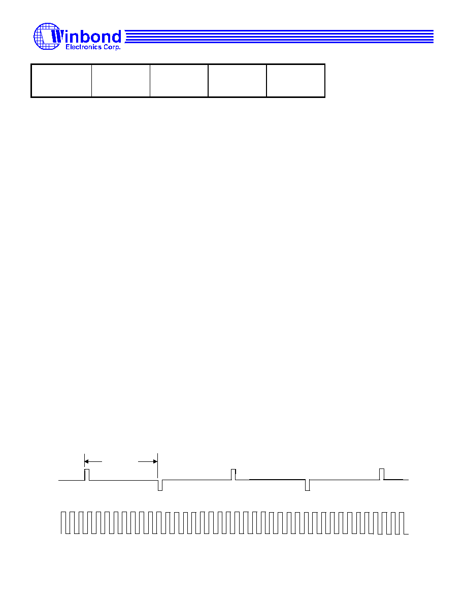
Preliminary Data Sheet
W6692 PCI ISDN S/T-Controller
Publication Release Date: Sep 30, 1999
Revision 0.9
-36 -
1
2
etc.
ONE
ZERO
ONE
ZERO
S1
ZERO
Q1
ZERO
7.2.7 Test Functions
The W6692 provides loop and test functions as follows:
- Digital loop via DLP bit in D_MODE register: In the layer 2 block, the transmitted 2B+D data are internally
looped (from HDLC transmitter to HDLC receiver), and in the PCM ports, the transmitted B channels are
internally looped (from PCM inputs to PCM outputs). The clock timings are generated internally and are
independent of the S bus timing. This loop function is used for test of PCM and higher layer functions, excluding
layer 1. After hardware reset, W6692 will power down if S bus is not connected or if there is no signal on the S
bus. In this case, the C/I command ECK must be issued to power up the chip.
- Analog loop via the C/I command EAL: The analog S interface transmitter is internally connected to the S
interface receiver. When the receiver has synchronized itself to the internal INFO 3 signal, the message "Test
Indication" or "Awake Test Indication" is delivered to the CIR register. No signal is transmitted over the S
interface.
In this mode, the S interface awake detector is enabled. Therefore if a level (INFO 2/ INFO 4) is detected on the S
interface, this will be reported by the "Awake Test Indication (ATI)" indication.
- Remote loopback via RLP bit in D_MODE register: The digital 2B data received from the S interface receiver is
loopbacked to the S interface transmitter. The D channel is not looped. When RLP is enabled, layer 1 D channel is
connected to HDLC port and DLP cannot be enabled.
- Transmission of special test signals via layer 1 command:
* Send Single Pulses (SSP): To send isolated single pulses of alternating polarity, with pulse width of one bit
time, 250 us apart, with a repetition frequency of 2 kHz.
* Send Continuous Pulses (SCP): To send continuous pulses of alternating polarity, with pulse width of bit time.
The repetition frequency is 96 kHz.
250 us
(a) Single pulses
(b) Continuous pulses

Preliminary Data Sheet
W6692 PCI ISDN S/T-Controller
Publication Release Date: Sep 30, 1999
Revision 0.9
-37 -
FIG.7.7 SSP AND SCP TEST SIGNALS
Preliminary Data Sheet
W6692 PCI ISDN S/T-Controller
Publication Release Date: Sep 30, 1999
Revision 0.9
-38 -
7.3 Serial Interface Bus
The 192 kbps S/T interface signal consists of two B channels (64 kbps each), one D channel (16 kbps) and other control
signals. The multiplexing/demultiplexing functions are carried out in the Serial Interface Bus (SIB) block. In addition, the B1
and B2 channels can be individually set to carry 64 kbps or 56 kbps traffic.
7.4 B Channel Switching
Each B channel in S/T bus or U transceiver can be individually programmed to connect to one of the three data ports : B
channel HDLC controller , PCM port 1 or PCM port 2. In addition, the PCM ports can be programmed to connect to the B
channel HDLC controller for voice recording/ retrieving from main memory in answering machine applications. In this case,
only extended transparent mode can be used.
The switching matrix is controlled by PXC bit in PCTL register and BSW1-0 bits in B1_MODE and B2_MODE registers as
follows :
A special mode is provided (BSW1-0 = 11B) in which case the PCM port can receive data from layer 1 and the HDLC receiver
can receive data from PCM port simultaneously. Here are the setting values of possible switching combinations shown as below.
PCM1 Receive Table
PXC
B1_SW[1:0]
B2_SW[1:0]
PCM1 Rx
0
00
xx
L1_B1
0
01
xx
L1_B1
0
10
xx
L2_B1
0
11
xx
PCM1
1
xx
00
L1_B2
1
xx
01
L1_B2
1
xx
10
L2_B2
1
xx
11
PCM2
Layer 1
/GCI
HDLC/
Layer 2
B1
HDLC/Layer 2
B2
PCM
TX/RX
PCM2
TX/RX
01
00
10
01
00
10
0
0
1
1
BSW1-0 bits
PXC bit
Layer 1
/GCI

Preliminary Data Sheet
W6692 PCI ISDN S/T-Controller
Publication Release Date: Sep 30, 1999
Revision 0.9
-39 -
PCM2 Receive Table
PXC
B1_SW[1:0]
B2_SW[1:0]
PCM2 Rx
0
xx
00
L1_B2
0
xx
01
L1_B2
0
xx
10
L2_B2
0
xx
11
PCM2
1
00
xx
L1_B1
1
01
xx
L1_B1
1
10
xx
L2_B1
1
11
xx
PCM1
Layer2-B1 Receive Table
PXC
B1_SW[1:0]
B2_SW[1:0]
L2_B1 Rx
x
00
xx
L1_B1
x
01
xx
L1_B1
0
10
xx
PCM1
1
10
xx
PCM2
x
11
xx
L1_B1
Layer2-B2 Receive Table
PXC
B1_SW[1:0]
B2_SW[1:0]
L2_B2 Rx
x
xx
00
L1_B2
x
xx
01
L1_B2
0
xx
10
PCM2
1
xx
10
PCM1
x
xx
11
L1_B2
Layer1-B1 Receive Table
PXC
B1_SW[1:0]
B2_SW[1:0]
L1_B1 Rx
x
00
xx
L2_B1
0
01
xx
PCM1
1
01
xx
PCM2
x
10
xx
High
x
11
xx
L2_B1
Layer1-B2 Receive Table
PXC
B1_SW[1:0]
B2_SW[1:0]
L1_B2 Rx
x
xx
00
L2_B2
0
xx
01
PCM2
1
xx
01
PCM1
x
xx
10
High
x
xx
11
L2_B2
Preliminary Data Sheet
W6692 PCI ISDN S/T-Controller
Publication Release Date: Sep 30, 1999
Revision 0.9
-40 -
7.5 PCM Port
There are two PCM ports in W6692. Each PCM port can connect to a PCM codec filter chip. These two PCM ports share the
same signals except for the frame synchronization clocks. The frame synchronization clocks (PFCK1-2) are 8 kHz and the bit
synchronization clock (PBCK) is 1.536 MHz. The bit data rate is 64 kbps per port.
7.6 D Channel HDLC Controller
There are two HDLC protocols that are used for ISDN layer 2 functions : LAPD and LAPB. Their frame formats are shown
below.
LAPB modulo 8 :
flag
(1 octet)
address
(1octet)
control
(1octet)
information
(0 or N octets)
FCS
(2 octets)
flag
(1 octet)
Control field bits
7
6
5
4
3
2
1
0
I frame
N(R)
P
N(S)
0
S frame
N(R)
P/F
S
S
0
1
U frame
M
M
M
P/F
M
M
1
1
LAPB modulo 128 :
flag
(1 octet)
address
(1octet)
control
(1 or 2 octets)
information
(0 or N octets)
FCS
(2 octets)
flag
(1 octet)
1st octet
2nd octet
Control field bits
7
6
5
4
3
2
1
0
7
6
5
4
3
2
1
0
I frame
N(S)
0
N(R)
P
S frame
X
X
X
X
S
S
0
1
N(R)
P/F
U frame
M
M
M P/F M
M
1
1
LAPD : modulo 128 only
flag
(1 octet)
address
(2 octets)
control
(2 octets)
information
(0 or N octets)
FCS
(2 octets)
flag
(1 octet)
1st octet
2nd octet
Control field bits
7
6
5
4
3
2
1
0
7
6
5
4
3
2
1
0
I frame
N(S)
0
N(R)
P/F

Preliminary Data Sheet
W6692 PCI ISDN S/T-Controller
Publication Release Date: Sep 30, 1999
Revision 0.9
-41 -
S frame
0
0
0
0
S
S
0
1
N(R)
P/F
U frame
M
M
M P/F M
M
1
1
7.6.1 D Channel Message Transfer Modes
The D channel HDLC controller operates in transparent mode.
Chracteristics:
- Receive frame address recognition
- Address comparison maskable bit-by-bit
- Flag generation / deletion
- Zero bit insertion/ deletion
- Frame Check Sequence (FCS) generation/ check with CRC_ITU-T
Note. The LAPD protocol uses the CRC_ITU-T for Frame Check Sequence. The polynominal is X
16
+ X
12
+ X
5
+ 1.
For address recognition, the W6692 provides four programmable registers for individual SAPI and TEI values, SAP1-2 and
TEI1-2, plus two fixed values for group SAPI and TEI, SAPG and TEIG. The SAPG equals FEH or FCH which corresponds to
SAPI = 63 for layer management procedure. The TEIG equals FFH which corresponds to TEI = 127 for automatic TEI
assignment procedure. The address combinations are :
- SAP1 + TEI1
- SAP1 + FFH
- SAP2 + TEI2
- SAP2 + FFH
- FEH (FCH) + TEI1
- FEH (FCH) + TEI2
- FEH (FCH) + FFH
The receive frame address comparisons can be disabled (masked) per bit basis with the D_SAM and D_TAM registers, but
comparisons with the SAPG or TEIG cannot be disabled.
7.6.2 Reception of Frames in D Channel
A 128-byte FIFO is provided in the receive direction. The data movement between receive FIFO and micro-processor is
handled by interrupts.
There are two interrupt sources: Receive Message Ready (D_RMR) and Receive Message End (D_RME). The D_RMR
interrupt indicates that at least 64 bytes of data have been received and the message/ frame is not ended. Upon D_RMR interrupt,

Preliminary Data Sheet
W6692 PCI ISDN S/T-Controller
Publication Release Date: Sep 30, 1999
Revision 0.9
-42 -
the microprocessor reads out 64 bytes of data from the FIFO. The D_RME interrupt indicates the last segment of a message or a
message with length
64 bytes has been received. The length of data is less than or equal to 64 and is specified in the D_RBCL
register.
If the length of the last segment of message is 64, only D_RME interrupt is generated and the RBC5-0 bits in D_RBCL register
are 000000B.
The data between the opening flag and the CRC field are stored in D_RFIFO. For LAPD frame, this includes the address field,
control field and information field.
When a D_RMR or D_RME interrupt is generated, the micro-processor must read out the data from D_RFIFO and issues the
Receive Message Acknowledgement command (D_CMDR: RACK bit) to explicitly acknowledge the interrupt. The
microprocessor must handle the interrupt before more than 64 bytes of data are received. This corresponds to a maximum
microprocessor reaction time of 32 ms at 16 kbps data rate.
If the microprocessor is late in handling the interrupt, the incoming additional bytes will result in a "data overflow" interrupt
and status bit.
7.6.3 Transmission of Frames in D Channel
A 128-byte FIFO is provided in the transmit direction. If the transmit FIFO is ready (which is indicated by a D_XFR interrupt),
the micro-processor can write up to 64 bytes of data into the FIFO and use the XMS command bit to start frame transmission.
The HDLC transmitter sends the opening flag first and then sends the data in the transmit FIFO.
The microprocessor must write the address, control and information field of a frame into the transmit FIFO.
Every time no more than 64 bytes of data are left in the transmit FIFO, the transmitter generates a D_XFR interrupt to request
another block of data. The microprocessor can then write further data to the transmit FIFO and enables the subsequent
transmission by issuing an XMS command.
If the data written to the FIFO is the last segment of a frame, the microprocessor issues the XME (Transmit Message End) and
XMS command bits to finish the frame transmission. The transmitter then transmits the data in the FIFO and appends CRC and
closing flag.
If the microprocessor fails to respond the D_XFR interrupt within a given time (32 ms), a data underrun condition will occur.
The W6692 will automatically reset the transmitter and send inter frame time fill pattern (all 1's) on D channel. The
microprocessor is informed about this condition via an XDUN (Transmit Data Underrun) interrupt in D_EXIR register. The
microprocessor must wait until transmit FIFO ready (via XFR interrupt ), re-write data, and issue XMS command to re-transmit
the data.
It is possible to abort a frame by issuing a D_CMDR:XRST (D channel Transmitter Reset) command. The XRST command
resets the transmitter and causes a transmit FIFO ready condition.

Preliminary Data Sheet
W6692 PCI ISDN S/T-Controller
Publication Release Date: Sep 30, 1999
Revision 0.9
-43 -
After the microprocessor has issued the XME command, the successful termination of transmission is indicated by an D_XFR
interrupt.
The inter-frame time fill pattern must be all 1's, according to ITU-T I.430.
Collisions which occur on the D channel of S interface will cause an D_EXIR:XCOL interrupt. A XRST (Transmitter Reset)
command must be issued and software must wait until transmit FIFO ready (via XFR interrupt), re-write data, and issue XMS
command to re-transmit the data.
7.7 B Channel HDLC Controller
There are two B channel HDLC controllers. Each B channel HDLC controller provides two operation modes :
- Transparent mode
characteristics :
* 2 byte address field
* Receive address comparison maskable bit-by-bit
* Data between opening flag and CRC (not included) stored in receive FIFO
* Flag generation/ deletion
* Frame Check Sequence generation/ check with CRC_ITU-T polynominal
* Zero bit insertion/ deletion
- Extended transparent mode
characteristics :
* All data transmitted/ received without modification
* No address comparison
* No flag generation/ detection
* No FCS generation/ check
* No bit stuffing
For PCM-HDLC connection, only extended transparent mode can be selected.
The data rate in B channel can be set at 64 kbps or 56 kbps by the B1_MODE (B2_MODE) : SW56 bit.
7.7.1 Reception of Frames in B Channel
A 128-byte FIFO is provided in the receive direction. The receive FIFO threshold can be set at 64 or 96 bytes by the Bn_MODE
register. If the number of received data reaches the threshold, a Receive Message Ready (RMR) interrupt will be generated.
The operations for reception of frames differ in each mode:

Preliminary Data Sheet
W6692 PCI ISDN S/T-Controller
Publication Release Date: Sep 30, 1999
Revision 0.9
-44 -
Transparent mode: The received frame address is compared with the contents in receive address registers. In addition, the
comparisons can be selectively masked bit-by-bit via address mask registers. Comparison is disabled when the corresponding
mask bit is "1".
In addition, flag recognition, CRC check and zero bit deletion are also performed. The result of CRC check is indicated in
Bn_STAR: CRCE bit. The data between opening flag and CRC field (not included) is stored in receive FIFO. Two interrupts are
used for the reception of data. The RMR interrupt in Bn_EXIR register indicates at least a threshold block of data have been put
in the receive FIFO. The RME interrupt in Bn_EXIR register indicates the end of frame has been received. The micro-processor
can read out a threshold length of data from receive FIFO at RMR interrupt, or all the data in receive FIFO at RME interrupt. At
each RMR/ RME interrupt, micro-processor must issue a Receive Message Acknowledgement(RACK) command to explicitly
acknowledge the interrupt.
The microprocessor reaction time for RMR/ RME interrupt depends on the FIFO threshold setting and B channel data rate. For
example, it is 8 ms if the FIFO threshold is 64 and the B channel data rate is 64 kbps.
If the microprocessor is late in handling the interrupt, the incoming additional bytes will result in a "data overflow" interrupt
and status bit.
Extended transparent mode: In this mode, all data received are stored in the receive FIFO without any modification. Every
time up to a threshold length of data has been stored in the FIFO, a Bn_RMR interrupt is generated.
In this mode, there is no RME interrupt.
The microprocessor must react to the RMR interrupt in time, otherwise a "data overflow" interrupt and status bit will be
generated.
7.7.2 Transmission of Frames in B Channel
A 128-byte FIFO is provided in the transmit direction. The FIFO threshold can be set at 64 or 96 bytes. The transmitter and
receiver use the same FIFO threshold setting.
The transmit operations differ in both modes:
Transparent mode:
In this mode, the following functions are performed by the transmitter automatically:
- Flag generation
- CRC generation
- Zero bit insertion
The fields such as address, control and information are provided by the microprocessor and are stored in transmit FIFO. To
start the frame transmission, the microprocessor issues a XMS (Transmit Message Start) command. The transmitter requests
another block of data via XFR interrupt when more than a threshold length of vacancies are left in the FIFO.The micro-processor
then writes up to a threshold length of data into the FIFO and activates the subsequent transmission of the frame by a XMS

Preliminary Data Sheet
W6692 PCI ISDN S/T-Controller
Publication Release Date: Sep 30, 1999
Revision 0.9
-45 -
command too. The microprocessor indicates the end of the frame transmission by issuing XME (Transmit Message End) and
XMS commands at the same time. The transmitter then transmits all the data left in the transmit FIFO and appends the CRC and
closing flag. After this, a XFR interrupt is generated.
The inter-frame time fill pattern can be programmed to 1's or flags.
During the frame transmission, the microprocessor reaction time for the XFR interrupt depends on the FIFO threshold setting
and B channel data rate. For example, it is 8 ms if the FIFO threshold is 64 and the B channel data rate is 64 kbps. If the
microprocessor fails to responds within the given reaction time, the transmit FIFO will be underrun. In this case, the W6692 will
automatically reset the transmitter and send the inter frame time fill pattern on B channel. The microprocessor is informed about
this via a Transmit Data Underrun interrupt (XDUN bit in Bn_EXIR register). The microprocessor must wait until transmit FIFO
ready (via XFR interrupt), re-write data, and issue XMS command to re-transmit the data.
The microprocessor can abort a frame transmission by issuing a Transmitter Reset command (XRES bit in Bn_CMDR
register). The XRES command resets the transmitter and sends inter frame time fill pattern on B channel. It also results in a
transmit pool ready condition.
Extended transparent mode:
All the data in the transmit FIFO are transmitted without any modification, i.e. no flags and CRCs are inserted, and no bit
stuffing is performed.
Transmission is started by a XMS command. The transmitter requests another block of data via XFR interrupt when more than
a threshold length of vacancies are left in the FIFO. The microprocessor reacts to this condition by writing up to a threshold
length of data into the transmit FIFO and issues a XMS command to continue the message transmission.
The microprocessor reaction time depends on the FIFO threshold setting and B channel data rate. For example, it is 8 ms if the
FIFO threshold is 64 and the B channel data rate is 64 kbps. If the microprocessor fails to respond within the given reaction time,
the transmit FIFO will hold no data to transmit. In this case, the W6692 will automatically reset the transmitter and send idle
channel pattern defined in Bn_IDLE register. The microprocessor is informed about this via a Transmit Data Underrun interrupt
(XDUN bit in Bn_EXIR register). The microprocessor must wait until transmit FIFO ready (via XFR interrupt), re-write data,
and issue XMS command to re-transmit the data.
7.8 GCI Mode Serial Interface Bus
The GCI is a generalization and enchancement of the general purpose, serial interface bus. The GCI bus offers capacity for the
transfer of maintenance information. In terminal applications, the GCI constitute a powerful backplane bus offering
sophisticated control capabilities for peripheral modules. The channel structure of the GCI mode is depicted below:
Channel Structure of the W6692 GCI Mode:
Preliminary Data Sheet
W6692 PCI ISDN S/T-Controller
Publication Release Date: Sep 30, 1999
Revision 0.9
-46 -
CH0
CH1
CH2
B1
B2
MON0
D C/I0
IC1
IC2
MON1 C/I1
C/I2
B1
B2
Monitor
D
C/I
MR
MX
1
st
Octet 2
nd
Octet 3
rd
Octet
4
th
Octet
FIG 7.8 GCI MODE CHANNEL STRUCTURE
GCI slave mode: connects to U transceiver such as PEB 2091, CH0 used only.
GCI master mode: connects to PSB 2165 ARCOFI, uses B1, B2, IC1 and IC2 for voice communication, uses MON1 for
programming, uses C/I1 for pins SA-SD access.
The GCI signals are:
DD/DU : 768 Kbps
DCL : 1.536 MHz
FSC : 8 KHz
7.8.1 GCI Mode C/I0 Channel Handling
The Command/Indication channel 0 carries real-time status information between the W6692 and another device connected to
the GCI bus interface.
One C/I0 channel conveys the commands and indications between a layer 1 device and layer 2 device. This C/I0 channel is
accessed via register CIR (in receive direction, layer 1 to layer 2) and register CIX (in transmit direction, layer 2 to layer 1). The
C/I code is 4-bit long.
�
In the receive direction, the code from layer 1 is continuously monitored, with an interrupt being generated anytime a
change occurs. A new code must be found in two consecutive GCI frames to be consided valid and to trigger a C/I code
change interrupt status (double last look criterion).
�
In the transmit direction, the code written in CIX is continuously transmitted in the channel.
7.8.2 GCI Mode Monitor Channel Handling
The Monitor channel protocol is a handshake protocol used for high speed information exchange between the W6692 and other
devices. The Monitor channel is necessary for:

Preliminary Data Sheet
W6692 PCI ISDN S/T-Controller
Publication Release Date: Sep 30, 1999
Revision 0.9
-47 -
�
Programming and controlling devices attached to the GCI interface.
�
Data exchange between two microprocessor systems attached to two different devices on one GCI backplane. Use of the
Monitor channel avoids the necessity of a dedicated serial communication path between two systems.
The Monitor channel operates on an asynchronous basis. While data transfers on the bus take place synchronized to frame sync,
the flow of data is controlled by a handshake procedure using the Monitor Channel Receiver (MOR) and Monitor Channel
Transmit (MOX) bits. When data is placed into the Monitor channel and the MX bit is activated. This data will be transmitted
repeatedly once per 8 KHz frame until the transfer is acknowledged via the MR bit.
The microprocessor may either enforce a 1 (idle state) in MR, MX by setting the control bit MRC or MXC (MOCR register) to
0, or enable the control of these bits internally by the W6692 according to the Monitor channel protocol. Thus, before a data
exchange can begin, the control bit MRC, or MXC should be set to 1 by the microprocessor.
The relevant status bits are:
�
For the reception of Monitor data: MDR (Monitor Channel Data Received )
MER (Monitor Channel End of Reception)
�
For the transmission of Monitor data: MDA (Monitor Channel Data Acknowledged )
MAB (Monitor Channel Data
Abort)
About the status bit MAC( Monitor Channel Transmit Active) indicates whether a transmission is progress.
�
If set MAC = 0, the previous transmission has been terminated. Before starting a transmission, the microprocessor should
verify that the transmitter is inactive.
�
If set MAC = 1, after having written data into the Monitor Transmit Channel (MOX) register, the microprocessor sets this
bit to 1. This enables the MX bit to go active (0), indicating the presence of valid Monitor data (contents of MOX) in the
corresponding frame.
The receiving device stores the Monitor byte in its MOR (Monitor Receive Register) and generates a MDR (Monitor Channel
Data Receive) interrupt status. Alerted by the MDR interrupt, the microprocessor reads the MOR register. When it is ready to
accept data, it sets the MR control bit MRC to 1 to enable the receiver to store succeeding Monitor channel bytes and
acknowledge them according to the Monitor channel protocol. In addition, it enables other Monitor channel interrupts by setting
Monitor Channel Interrupt Enable to 1.
The first Monitor channel byte is acknowledged by the receiving device setting the MR bit to 0. This causes a MDA (Monitor
Channel Data Acknowledge) interrupt status at the transmitter. A new Monitor channel data byte can now be written by the
microprocessor in MOX register. The MX bit is still in the active (0) state. The transmitter indicates a new byte in the Monitor
channel by returning the MX bit active after sending it once in the inactive state. The receiver stores the Monitor channel byte
in MOR register and generates a new MDR interrupt status. When the microprocessor has read the MOR register , the receiver
acknowledges the data by returning the MR bit active after sending it once in the inactive state. This in turn causes the
transmitter to generate a MDA interrupt status. This
MDA interrupt
write data
MDR interrupt
read data
MDA
interrupt
handshake procedure is repeated as long as the transmitter has data to send.
When the last byte has been acknowledged by the receiver (MDA interrupt status), the microprocessor sets the Monitor channel
Transmit Control bit MXC to 0. This enforces an inactive (1) state in the MX bit. Two frames of MX inactive signifies the end of
a message. Thus, a MER (Monitor channel End of Reception) interrupt status is generated by the receiver when the MX is
received in the inactive state in two consecutive frames. As a result, the microprocessor sets the MR control bit MRC to 0, which
in turn enforces an inactive state in the MR bit. This marks the end of the transmittion, making the MAC (Monitor channel
Active) bit return to 0.
Preliminary Data Sheet
W6692 PCI ISDN S/T-Controller
Publication Release Date: Sep 30, 1999
Revision 0.9
-48 -
During a transmission process, it is possible for the receiver to ask a transmission to be aborted by sending an inactive MR bit
value in two consecutive frames. This is effected by the microprocessor writing the MR control bit MRC to 0. An aborted
transmission is indicated by a MAB (Monitor Channel Data Abort) interrupt status at the transmitter.
7.9 PCI/MP Interface Circuit
7.9.1 PCI Slave Mode And Configuration Serial EEPROM
W6692 implements slave (target) mode function which meets PCI local bus specification revision 2.2 and PCI Power
Management 1.1. All the signals are 5V, 33 MHz compatible. A single function, type 00h configuration header is implemented
for control of the internal ISDN device and external peripheral device(s). Memory mode and/or IO mode can be used for W6692's
register access.
After power on reset, W6692 starts to read configuration data from serial EEPROM. The first word read is Vendor ID, if it
equals FFFFH, a EEPROM empty condition is assumed and chip's internal default configuration data is used, otherwise, the
configuration data stored in serial EEPROM is used. The default configuration data is as follows:
Vendor ID
: 1050H (Winbond's ID)
Device ID
: 6692H
Class Code
: 02 04 00H
Revision ID
: 00H
Interface Code
: 00H
Subclass Code
: 04H
Base Class Code
: 02H
Subsystem Vendor ID
: FFFFH
Subsystem ID
: FFFFH
Memory Base Address Register
: Enabled and Implemented at 10H
IO Base Address Register
: Enabled and Implemented at 14H
A 9346/93C46 type serial EEPROM is used for configuration data storage. The EEPORM's data layout is as follows :
Address/Byte
1
0
0
H
Vendor ID
2
H
Device ID
4
H
Interface Code
Revision ID
6
H
Base Class Code
Subclass Code
8
H
Subsystem Vendor ID
A
H
Subsystem ID
C
H
Address Register Control
E
H
PMC
FIG.7.9 SERIAL EEPROM DATA LAYOUT
Preliminary Data Sheet
W6692 PCI ISDN S/T-Controller
Publication Release Date: Sep 30, 1999
Revision 0.9
-49 -
Word 6 (Bytes 12,13) is for Address Register Control, its format is :
15
14
13
12
0
MEN
IEN
PRE
not used
The Address Register Control determines the PCI address register's implementation. Bit 13 is the prefetchable bit in Memory
Base Address register.
MEN
IEN
PCI Configuration Space
Location 10H
PCI Configuration Space
Location 14H
Bit 13
used ?
1
1
Memory Base Address Reg.
IO Base Address Reg.
yes
1
0
Memory Base Address Reg.
Not Implemented
yes
0
1
IO Base Address Reg.
Not Implemented
no
0
0
Not Implemented
Not Implemented
no
EEPROM empty Memory Base Address Reg.
IO Base Address Reg.
PRE=0
In all cases, Memory Base Address register allocates 4096 byte spaces and IO Base Address register allocates 256 byte space.
Word 7 is Power Management Capability register. It replaces the chip's default value if EEPROM is not empty.
W6692 provides an EPCTL register for on-board access of the serial EEPROM. Software is responsible for creation of the serial
EEPROM waveform and timing and can read, write or erase the EEPROM's content.
7.9.2 8-bit Microprocessor Interface
At power up, the reset pin RST# must be asserted to initialize the chip. At rising edge of RST#, data at CLK pin determines the
operation modes: clock for PCI mode, HIGH for Intel bus mode, LOW for Motorola bus mode.
7.10 Peripheral Control
In PCI card with POTS application, the peripheral devices such as CODEC, DTMF and SLIC can be directly controlled by
W6692, therefore eliminates the need for another PCI controller chip. The peripheral control function includes timer, interrupt
inputs and programmable IOs or microprocessor interface.
There are two timers implemented in W6692: TIMR1 and TIMR2. TIMR1 is a long period timer whcich can be used to control
the cadence of ring tone. TIMR2 is a short period timer which can be used to generate the 20 Hz ring signal.
Address Interrupt status Interrupt mask
Output pin Period
Cyclic
TIMR1
10H
DEXIR:T1EXP DEXIM:T1EXP No
(0..127)x 100 ms
yes (CNT=7)
TIMR2
4CH
DEXIR:TIN2
DEXIM:TIN2
TOUT2
(1..63) ms
yes(TMD=1)
There are two interrupt inputpins : XINTIN0, XINTIN1. Whenever signal level changes (eith rising or falling), a maskable
interrupt is generated which in turn will make an interrupt request on PCI bus if it is unmasked. The interrupt status bits are
ISTA:XINT0, ISTA:XINT1. The mask bits are IMASK:XINT0, IMASK:XINT1. In addition, the signal level can be read at bits
SQR:XIND0, SQR;XIND1. These pins can be used for monitor of SLIC hook state and/or DTMF data valid status.

Preliminary Data Sheet
W6692 PCI ISDN S/T-Controller
Publication Release Date: Sep 30, 1999
Revision 0.9
-50 -
The IO interface can be programmed as simple IO (PCTL:XMODE=0) or 8-bit microprocessor interface (PCTL:XMODE=1).
As simple IOs, the pin data are accessed via XADDR and XDATA registers. The register data is output on the pin if its output
enable bit is set, the read data reflects the current level of pin. In this mode, a maximum of 11 IO ports are supported.
If programmed as 8-bit microprocessor mode, an 8-bit multiplexed bus is used to control peripheral deveces. The address and
data are multiplexed on XAD7-0. XALE is used for address latch and XRDB, XWRB are used for read/write strobe. To access
peripheral device, first write the desired address in XADDR register and then read/write data at XDATA register. In this mode, a
maximum of 256 byte ports can be supported by adding some glue TTLs on board.

Preliminary Data Sheet
W6692 PCI ISDN S/T-Controller
Publication Release Date: Sep 30, 1999
Revision 0.9
-51 -
8. REGISTER DESCRIPTIONS
8.1 Chip Control and D_ch HDLC controller
TABLE 8.1 REGISTER ADDRESS MAP: CHIP CONTROL AND D CHANNEL HDLC
Section Offset
Access Register Name
Description
8.1.1 00/00
R
D_RFIFO
D channel receive FIFO
8.1.2 04/01
W
D_XFIFO
D channel transmit FIFO
8.1.3 08/02
R/W D_CMDR
D channel command register
8.1.4 0C/03
R/W D_MODE
D channel mode control
8.1.5 10/04
R/W TIMR1
Timer 1
8.1.6 14/05
R_clear ISTA
Interrupt status register
8.1.7 18/06
R/W IMASK
Interrupt mask register
8.1.8 1C/07
R_clear D_EXIR
D channel extended interrupt
8.1.9 20/08
R/W D_EXIM
D channel extended interrupt mask
8.1.10 24/09
R
D_XSTA
D channel transmit status
8.1.11 28/0A
R
D_RSTA
D channel receive status
8.1.12 2C/0B
R/W D_SAM
D channel address mask 1
8.1.13 30/0C
R/W D_SAP1
D channel individual SAPI 1
8.1.14 34/0D
R/W D_SAP2
D channel individual SAPI 2
8.1.15 38/0E
R/W D_TAM
D channel address mask 2
8.1.16 3C/0F
R/W D_TEI1
D channel individual TEI 1
8.1.17 40/10
R/W D_TEI2
D channel individual TEI 2
8.1.18 44/11
R
D_RBCH
D channel receive frame byte count high
8.1.19 48/12
R
D_RBCL
D channel receive frame byte count low
8.1.20 4C/13
R/W TIMR2
Timer 2
8.1.21 50/14
R/W L1_RC
GCI layer 1 ready code
8.1.22 54/15
R/W CTL
Control register
8.1.23 58/16
R
CIR
Command/Indication receive
8.1.24 5C/17
R/W CIX
Command/Indication transmit
8.1.25 60/18
R
SQR
S/Q channel receive register
8.1.26 64/19
R/W SQX
S/Q channel transmit register
8.1.27 68/1A
R/W PCTL
Peripheral control register
8.1.28 6C/1B
R
MO0R
Monitor receive channel 0
8.1.29 70/1C
R/W MO0X
Monitor transmit channel 0
8.1.30 74/1D
R_clear MO0I
Monitor channel 0 interrupt
8.1.31 78/1E
R/W MO0C
Monitor channel 0 control register

Preliminary Data Sheet
W6692 PCI ISDN S/T-Controller
Publication Release Date: Sep 30, 1999
Revision 0.9
-52 -
8.1.32 7C/1F
R/W GCR
GCI mode control/ status register
8.1.33 F4/3D
R/W XADDR
Peripheral address register
8.1.34 F8/3E
R/W XDATA
Peripheral data register
8.1.35 FC/3F
R/W EPCTL
Serial EEPROM control
8.1.36 6D/40
R
MO1R
Monitor receive channel 1
8.1.37 71/41
R/W MO1X
Monitor transmit channel 1
8.1.38 75/42
R_clear MO1I
Monitor channel 1 interrupt
8.1.39 79/43
R/W MO1C
Monotor channel 1 control
8.1.40 6E/44
R
IC1R
GCI IC1 receive
8.1.41 72/45
R/W IC1X
GCI IC1 transmit
8.1.42 6F/46
R
IC2R
GCI IC2 receive
8.1.43 73/47
R/W IC2X
GCI IC2 transmit
8.1.44 7D/48
R
CI1R
GCI CI1 indication
8.1.45 7E/49
R/W CI1X
GCI CI1 command
8.1.46 76/4A
R_clear GCI_EXIR
GCI extended interrupt
8.1.47 7A/4B
R/W GCI_EXIM
GCI extended interrupt mask
TABLE 8.2 REGISTER SUMMARY: CHIP CONTROL AND D CHANNEL HDLC
Offset
R/W Name
7
6
5
4
3
2
1
0
00/00 R
D_RFIFO
04/01 W
D_XFIFO
08/02 R/W D_CMDR
RACK
RRST
STT1
XMS
XME
XRST
0C/03 R/W D_MODE
0
RACT
XACTB 0
PMES
MFD
DLP
RLP
10/04 R/W TIMR1
T1MD
CNT6
CNT5
CNT4
CNT3
CNT2
CNT1
CNT0
14/05 R_clr ISTA
D_RMR D_RME D_XFR XINT1
XINT0
D_EXI B1_EXI
B2_EXI
18/06 R/W IMASK
D_RMR D_RME D_XFR XINT1
XINT0
D_EXI B1_EXI
B2_EXI
1C/07 R_clr D_EXIR
RDOV
XDUN
XCOL
TIN2
GCI
ISC
T1EXP
0
20/08 R/W D_EXIM
RDOV
XDUN
XCOL
TIN2
GCI
ISC
T1EXP
1
24/09 R
D_XSTA
XDOW
XBZ
DRDY
28/0A R
D_RSTA
RDOV
CRCE
RMB
2C/0B R/W D_SAM
SAM7
SAM6
SAM5
SAM4
SAM3
SAM2 SAM1
SAM0
30/0C R/W D_SAP1
SA17
SA16
SA15
SA14
SA13
SA12
SA11
SA10
34/0D R/W D_SAP2
SA27
SA26
SA25
SA24
SA23
SA22
SA21
SA20
38/0E R/W D_TAM
TAM7
TAM6
TAM5
TAM4
TAM3
TAM2 TAM1
TAM0
3C/0F R/W D_TEI1
TA17
TA16
TA15
TA14
TA13
TA12
TA11
TA10
40/10 R/W D_TEI2
TA27
TA26
TA25
TA24
TA23
TA22
TA21
TA20
44/11 R
D_RBCH
VN1
VN0
LOV
RBC12
RBC11
RBC10 RBC9
RBC8
48/12 R
D_RBCL
RBC7
RBC6
RBC5
RBC4
RBC3
RBC2
RBC1
RBC0
4C/13 W
TIMR2
TMD
TIDLE
TCN5
TCN4
TCN3
TCN2
TCN1
TCN0

Preliminary Data Sheet
W6692 PCI ISDN S/T-Controller
Publication Release Date: Sep 30, 1999
Revision 0.9
-53 -
Offset
R/W Name
7
6
5
4
3
2
1
0
50/14 R/W L1_RC
RC3
RC2
RC1
RC0
54/15 R/W CTL
0
0
SRST
0
OPS1
OPS0
58/16 R
CIR
SCC
ICC
CODR3 CODR2 CODR1
CODR0
5C/17 R/W CIX
CODX3 CODX2 CODX1
CODX0
60/18 R
SQR
XIND1
XIND0
MSYN
SCIE
S1
S2
S3
S4
64/19 R/W SQX
SCIE
Q1
Q2
Q3
Q4
68/1A R/W PCTL
OE5
OE4
OE3
OE2
OE1
OE0
XMODE PXC
6C/1B R
MO0R
70/1C R/W MO0X
74/1D R_clr MO0I
MDR0
MER0 MDA0
MAB0
78/1E R/W MO0C
MRIE0
MRC0 MXIE0
MXC0
7C/1F R/W GCR
MAC0
MAC1
TLP
GRLP
SPU
PD
GMODE
F4/3D R/W XADDR
XA7
/IO7
XA6
/IO6
XA5
/IO5
XA4
/IO4
XA3
/IO3
XA2
/IO2
XA1
/IO1
XA0
/IO0
F8/3E R/W XDATA
XD7
XD6
XD5
XD4
XD3
XD2
/IO10
XD1
/IO9
XD0
/IO8
FC/3F R/W EPCTL
EPSDI
EN
SK
CS
SDO
6D/40 R
MO1R
71/41 R/W MO1X
75/42 R_clr MO1I
MDR1
MER1 MDA1
MAB1
79/43 R/W MO1C
MRIE1
MRC1 MXIE1
MXC1
6E/44 R
IC1R
IC1_7
IC1_6
IC1_5
IC1_4
IC1_3
IC1_2
IC1_1
IC1_0
72/45 R/W IC1X
IC1_7
IC1_6
IC1_5
IC1_4
IC1_3
IC1_2
IC1_1
IC1_0
6F/46 R
IC2R
IC2_7
IC2_6
IC2_5
IC2_4
IC2_3
IC2_2
IC2_1
IC2_0
73/47 R/W IC2X
IC2_7
IC2_6
IC2_5
IC2_4
IC2_3
IC2_2
IC2_1
IC2_0
7D/48 R
CI1R
CI1R_6 CI1R_5 CI1R_4 CI1R_3 CI1R_2 CI1R_1 MR
MX
7E/49 R/W CI1X
CI1X_6 CI1X_5 CI1X_4 CI1X_3 CI1X_2 CI1X_1 MR
MX
76/4A R_clr GCI_EXIR
0
0
0
MO1C
MO0C
IC1
IC2
CI1
7A/4B R/W GCI_EXIM 1
1
1
MO1C
0
IC1
IC2
CI1
8.1.1 D_ch receive FIFO D_RFIFO Read Address 00H/00H
The D_RFIFO has a length of 128 bytes.
After a D_RMR interrupt, exactly 64 bytes are available.
After a D_RME interrupt, the number of bytes available equals RBC5-0 bits in the D_RBCL register.
8.1.2 D_ch transmit FIFO D_XFIFO Write Address 04H/01H

Preliminary Data Sheet
W6692 PCI ISDN S/T-Controller
Publication Release Date: Sep 30, 1999
Revision 0.9
-54 -
The D_XFIFO has a length of 128 bytes.
After an D_XFR interrupt, up to 64 bytes of data can be written into this FIFO for transmission. At the first time, up to 128
bytes of data can be written.
8.1.3 D_ch command register D_CMDR Read/Write Address 08H/02H
Value after reset: 00H
7
6
5
4
3
2
1
0
RACK
RRST
STT1
XMS
XME
XRST
RACK Receive Acknowledge
After a D_RMR or D_RME interrupt, the processor must read out the data in D_RFIFO and then sets this bit to acknowledge
the interrupt.
RRST Receiver Reset
Setting this bit resets the D_ch HDLC receiver and clears the D_RFIFO data.
STT1 Start Timer 1
The timer 1 is started when this bit is set to one. The timer is stopped when it expires or by a write of the TIMR1 register.
XMS Transmit Message Start/Continue
Setting this bit will start or continue the transmission of a frame. The opening flag is automatically added by the HDLC
controller.
XME Transmit Message End
Setting this bit indicates the end of frame transmission.. The D_ch HDLC controller automatically appends the CRC and the
closing flag after the data transmission.
Note: If the frame
64 bytes, XME plus XMS commands must be issued at the same time.
XRST Transmitter Reset
Setting this bit resets the D_ch HDLC transmitter and clears the D_XFIFO. The transmitter will send inter frame time fill
pattern (which is 1's) immediately. This command also results in a transmit FIFO ready condition.
A read of this register returns the last written value.
8.1.4 D_ch Mode Register D_MODE Read/Write Address 0CH/03H
Value after reset : 00H

Preliminary Data Sheet
W6692 PCI ISDN S/T-Controller
Publication Release Date: Sep 30, 1999
Revision 0.9
-55 -
7
6
5
4
3
2
1
0
0
RACT XACTB
0
PMES
MFD
DLP
RLP
RACT Receiver Active
Setting this bit activates the D_ch HDLC receiver. This bit can be read. The receiver must be in active state in order to receive
data.
XACTB Transmitter Active
Resetting this bit activates the D_ch HDLC transmitter. This bit can be read. The transmitter must be in active state in order to
transmit data. Note this bit is active LOW.
PMES PME Trigger Select
0 : PCI power management event triggered by reception of D channel HDLC flag
1 : PCI power management event triggered by layer 1 becomes active
MFD Multiframe Disable
This bit is used to enable or disable the multiframe structure on S/T interface :
0 : Multiframe is enabled
1 : Multiframe is disabled
DLP Digital Loopback
Setting this bit activates the digital loopback function. The transmitted digital 2B+D channels are looped to the received 2B+D
channels. Note that after hardware reset, the internal clocks will turn off if the S bus is not connected or if there is no signal on
the S bus. In this case, the C/I command ECK must be issued to enable loopback function.
RLP Remote Loopback
Setting this bit to "1" activates the remote loopback function. The received 2B channels from the S interface are looped to the
transmitted 2B channels of S interface. The D channel is not looped in this loopback function.
Bits 7, 4, 3 Reserved
These bits are removed. The write values are don't care, but are read as zero.
8.1.5 Timer 1 Register TIMR1 Read/Write Address 10H/04H
Value after reset : 00H
7
6
5
4
3
2
1
0
T1MD
CNT6
CNT5
CNT4
CNT3
CNT2
CNT1
CNT0

Preliminary Data Sheet
W6692 PCI ISDN S/T-Controller
Publication Release Date: Sep 30, 1999
Revision 0.9
-56 -
T1MD Timer1 Mode
0 = Single mode: The timer counts once and generates a TEXP interrupt when expires.
1 = Periodical mode: The timer counts periodically and generates an interrupt at each expiration.
CNT6-0 Count Value
The expiration time is defined as:
T1 = CNT[6:0] * 0.1 second
This register can be read only after the timer has been started. The read value indicates the timer's current count value. In case
layer 1 is not activated, a C/I command "ECK" must be issued in addition to the STT1 command to start the timer.
8.1.6 Interrupt Status Register ISTA Read_clear Address 14H/05H
Value after reset : 00H
7
6
5
4
3
2
1
0
D_RMR
D_RME
D_XFR
XINT1
XINT0
D_EXI
B1_EXI
B2_EXI
D_RMR D_ch Receive Message Ready
A 64-byte data is available in the D_RFIFO. The frame is not complete yet.
D_RME D_ch Receive Message End
The last part of a frame with length > 64 bytes or a whole frame with length
64 bytes has been received. The whole frame
length is obtained from D_RBCH + D_RBCL registers. The length of data in the D_RFIFO equals:
data length = RBC5-0 if RBC5-0
0
data length = 64 if RBC5-0 =0
D_XFR D_ch Transmit FIFO Ready
This bit indicates that the transmit FIFO is ready to accept data. Up to 64 bytes of data can be written into the D_XFIFO.
An D_XFR interrupt is generated in the following cases :
- After an XMS command, when
64 bytes of XFIFO is empty
- After an XMS together with an XME command is issued, when the whole frame has been transmitted
- After an XRST command
- After hardware reset
XINT1 XINTIN1 Interrupt
This bit indicates that level change occurs at XINTIN1 pin. Both positive and negative edges will cause an interrupt.
XINT0 XINTIN1 Interrupt
This bit indicates that level change occurs at XINTIN0 pin. Both positive and negative edges will cause an interrupt.

Preliminary Data Sheet
W6692 PCI ISDN S/T-Controller
Publication Release Date: Sep 30, 1999
Revision 0.9
-57 -
D_EXI D_ch Extended Interrupt
This bit indicates that at least one interrupt bit has been set in D_EXIR register.
B1_EXI B1_ch Extended Interrupt
This bit indicates that at least one interrupt bit has been set in B1_EXIR register.
B2_EXI B2_ch Extended Interrupt
This bit indicates that at least one interrupt bit has been set in B2_EXIR register.
Note : A read of the ISTA register clears all bits except D_EXI, B1_EXI and B2_EXI bits. D_EXI bit is cleared when all bits
in D_EXIR register are cleared. B1_EXI bit is cleared by reading B1_EXI register and B2_EXI bit is cleared by reading
B2_EXIR register.
8.1.7 Interrupt Mask Register IMASK R/W Address 18H/06H
Value after reset: FFH
7
6
5
4
3
2
1
0
D_RMR
D_RME
D_XFR
XINT1
XINT0
D_EXI
B1_EXI
B2_EXI
Setting the bit to "1" masks the corresponding interrupt source in ISTA register. Masked interrupt status bits are read as zero.
They are internally stored and pending until the mask bits are zero.
Setting the D_EXI, B1_EXI or B2_EXI bit to "1" masks all the interrupts in D_EXIR, B1_EXIR or B2_EXIR register,
respectively.
8.1.8 D_ch Extended Interrupt Register D_EXIR Read_clear Address 1CH
Value after reset: 00H
7
6
5
4
3
2
1
0
RDOV XDUN XCOL
TIN2
GCI
ISC
T1EXP
0
RDOV Receive Data Overflow
Frame overflow (too many short frames) or data overflow occurs in the receive FIFO. In data overflow, the incoming data will
overwrite the data in the receive FIFO. If RDOV interrupt occurs, software has to reset the receiver and discard the data received.
XDUN Transmit Data Underrun
This interrupt indicates the D_XFIFO has run out of data. In this case, the W6692 will automatically reset the transmitter and
send the inter frame time fill pattern (all 1's) on D channel. The microprocessor must wait until transmit FIFO ready (via XFR
interrupt), re-write data, and issue XMS command to re-transmit the data.

Preliminary Data Sheet
W6692 PCI ISDN S/T-Controller
Publication Release Date: Sep 30, 1999
Revision 0.9
-58 -
XCOL Transmit Collision
This bit indicates a collision on the S-bus has been detected. A XRST command must be issued and software must wait until
transmit FIFO ready (via XFR interrupt), re-write data, and issue XMS command to re-transmit the data.
TIN2 Timer 2 Expiration
This bit is set when Timer 2 counts down to zero.
GCI GCI Interrupt
This bit is set when at least one bit is set in GCI_EXIR register.
ISC Indication or S Channel Change
A change in the layer 1 indication code or multiframe S channel has been detected. The actual value can be read from CIR or
SQR registers.
T1EXP Timer 1 Expiration
Expiration occurs in the Timer 1.
.
8.1.9 D_ch Extended Interrupt Mask Register D_EXIM Read/Write Address 20H/08H
Value after reset: FFH
7
6
5
4
3
2
1
0
RDOV XDUN XCOL
TIN2
GCI
ISC
T1EXP
1
Setting the bit to "1" masks the corresponding interrupt source in D_EXIR register. Masked interrupt status bits are read as
zero. They are internally stored and pending until the mask bits are zero.
All the interrupts in D_EXIR will be masked if the IMASK:D_EXI bit is set to "1".
8.1.10 D_ch Status Register D_XSTA Read Address 24H/09H
Value after reset: 00H
7
6
5
4
3
2
1
0
XDOW
XBZ
DRDY
XDOW Transmit Data Overwritten
At least one byte of data has been overwritten in the D_XFIFO. This bit is set by data overwritten condition and is cleared only
by XRST command.
XBZ Transmitter Busy

Preliminary Data Sheet
W6692 PCI ISDN S/T-Controller
Publication Release Date: Sep 30, 1999
Revision 0.9
-59 -
This bit indicates the D_HDLC transmitter is busy. The XBZ bit is active from the transmission of opening flag to the
transmission of closing flag.
DRDY D Channel Ready
This bit indicates the status of layer 1 D channel.
0: The layer 1 D channel is not ready. No transmission is allowed.
1: The layer 1 D channel is ready. Layer 2 can transmit data to layer 1.
8.1.11 D_ch Receive Status Register D_RSTA Read Address 28H/0AH
Value after reset: 20H
7
6
5
4
3
2
1
0
RDOV CRCE
RMB
RDOV Receive Data Overflow
A "1" indicates that the D_RFIFO is overflow. The incoming data will overwrite data in the receive FIFO. The data overflow
condition will set both the status and interrupt bits. It is recommended that software must read the RDOV bit after reading data
from D_RFIFO at RMR or RME interrupt. The software must abort the data and issue a RRST command to reset the receiver if
RDOV = 1. The frame overflow condition will not set this bit.
CRCE CRC Error
This bit indicates the result of frame CRC check:
0: CRC correct
1: CRC error
RMB Receive Message Aborted
A "1" means that a sequence of seven 1's was received and the frame is aborted. Software must issue RRST command to reset
the receiver.
Note: Normally D_RSTA register should be read by the microprocessor after a D_RME interrupt. The contents of D_RSTA are
valid only after a D_RME interrupt and remain valid until the frame is acknowledged via a RACK bit.
8.1.12 D_ch SAPI Address Mask D_SAM Read/Write Address 2CH/0BH
Value after reset: 00H
7
6
5
4
3
2
1
0

Preliminary Data Sheet
W6692 PCI ISDN S/T-Controller
Publication Release Date: Sep 30, 1999
Revision 0.9
-60 -
SAM7
SAM6
SAM5
SAM4
SAM3
SAM2
SAM1
SAM0
This register masks(disables) the first byte address comparison of the incoming frame. If the mask bit is "1" the corresponding
bit comparisons with D_SAP1, D_SAP2 are disabled. Comparison with SAPG is always performed.
Note : For the LAPD frame, the least significant two bits are the C/R bit and EA =0 bit. It is suggested that the comparison
with C/R bit be masked. EA=0 for two octet address frame e.g LAPD, EA=1 for one octet address frame.
8.1.13 D_ch SAPI1 Register D_SAP1 Read/Write Address 30H/0CH
Value after reset: 00H
7
6
5
4
3
2
1
0
SA17
SA16
SA15
SA14
SA13
SA12
SA11
SA10
This register contains the first choice of the first byte address of received frame. For LAPD frame, SA17 - SA12 is the SAPI
value, SA11 is C/R bit and SA10 is zero.
8.1.14 D_ch SAPI2 Register D_SAP2 Read/Write Address 34H/0DH
Value after reset: 00H
7
6
5
4
3
2
1
0
SA27
SA26
SA25
SA24
SA23
SA22
SA21
SA20
This register contains the second choice of the first byte address of received frame. For LAPD frame, SA27 - SA22 is the SAPI
value, SA21 is C/R bit and SA20 is zero.
8.1.15 D_ch TEI Address Mask D_TAM Read/Write Address 38H/0EH
Value after reset: 00H
7
6
5
4
3
2
1
0
TAM7 TAM6
TAM5 TAM4 TAM3 TAM2
TAM1 TAM0
This register masks (disables) the second byte address comparison of the incoming frame. If the mask bit is "1" the
corresponding bit comparisons with D_TEI1, D_TEI2 are disabled. Comparison with TEIG is always performed.
Note : For the LAPD frame, the least significant bit is the EA =1 bit.

Preliminary Data Sheet
W6692 PCI ISDN S/T-Controller
Publication Release Date: Sep 30, 1999
Revision 0.9
-61 -
8.1.16 D_ch TEI1 Register D_TEI1 Read/Write Address 3CH/0FH
Value after reset: 00H
7
6
5
4
3
2
1
0
TA17
TA16
TA15
TA14
TA13
TA12
TA11
TA10
TA17 - TA10
This register contains the first choice of the second byte address of received frame. For LAPD frame, TA17 - TA11 is the TEI
value, TA10 is EA = 1.
8.1.17 D_ch TEI2 Register D_TEI2 Read/Write Address 40H/10H
Value after reset: 00H
7
6
5
4
3
2
1
0
TA27
TA26
TA25
TA24
TA23
TA22
TA21
TA20
TA27 - TA20
This register contains the second choice of the second byte address of received frame. For LAPD frame, TA27 - TA21 is the
TEI value, TA20 is EA = 1.
8.1.18 D_ch Receive Frame Byte Count High D_RBCH Read Address 44H/11H
Value after reset: 00H
7
6
5
4
3
2
1
0
VN1
VN0
LOV
RBC12 RBC11 RBC10 RBC9
RBC8
VN1-0 Chip Version Number
This is the chip version number. It is read as 01B.
LOV Length Overflow
A "1" in this bit indicates
8192 bytes are received and the frame is not yet complete. This bit is valid only after an D_RME
interrupt and remains valid until the frame is acknowledge via the RACK command.
RBC12-8 Receive Byte Count
Four most significant bits of the total frame length. These bits are valid only after an D_RME interrupt and remain valid until the
frame is acknowledge via the RACK command.

Preliminary Data Sheet
W6692 PCI ISDN S/T-Controller
Publication Release Date: Sep 30, 1999
Revision 0.9
-62 -
8.1.19 D_ch Receive Frame Byte Count Low D_RBCL Read Address 48H/12H
Value after reset: 00H
7
6
5
4
3
2
1
0
RBC7
RBC6
RBC5
RBC4
RBC3
RBC2
RBC1
RBC0
RBC7-0 Receive Byte Count
Eight least significant bits of the total frame length. Bits RBC5-0 also indicate the length of the data currently available in
D_RFIFO. These bits are valid only after an D_RME interrupt and remain valid until the frame is acknowledged via the RACK
command.
8.1.20 Timer 2 TIMR2 Write Address 4CH/13H
Value after reset : 00H
7
6
5
4
3
2
1
0
TMD
TIDLE TCN5
TCN4
TCN3
TCN2
TCN1
TCN0
TMD Timer 2 Mode
0: One shot count down mode. The timer starts when it is written a non-zero count value and stops when it reaches zero.
1: Cyclic timer mode. The timer starts when it is written a non-zero count value and counts cyclically (periodically) with the
count value.
In both cases, a maskable interrupt TIN2 is generated every time the timer reaches zero. When timer starts, pin TOUT2
changes to HIGH and toggles every half count time. Therefore, the period of TOUT2 equals count value.
In both cases, timer counts with the new value if it is written again before expiration.
The timer is stopped when it expires (TMD=0), or by writting zero count value (TMD=0 or 1).
TIDLE TOUT2 Idle
This bit defines value of TOUT2 pin when timer if off.
TCN5-0 Timer 2 Count Value
0: Timer is off.
1-63: Timer count value in unit of ms.
8.1.21 Layer 1_Ready Code L1_RC Read/Write Address 50H/14H
Value after reset: 0CH
7
6
5
4
3
2
1
0
RC3
RC2
RC1
RC0
Preliminary Data Sheet
W6692 PCI ISDN S/T-Controller
Publication Release Date: Sep 30, 1999
Revision 0.9
-63 -
RC3-0 Ready Code
When GCI bus is being enabled, these four programmable bits are allowed to program different Layer 1_Ready Code (AI:
Activation Indication) by user. For example: Siemens PEB2091: AI=1100, Motorola MC145572: AI=1100.
8.1.22 Control Register CTL Read/Write Address 54H/15H
Value after reset : 00H
7
6
5
4
3
2
1
0
0
0
SRST
0
OPS1
OPS0
SRST Software Reset
When this bit is set to "1", a software reset signal is activated. The effects of this reset signal are equivalent to the hardware
reset pin , except that it does not reset the PCI interface circuit.
This bit is not auto-clear, the software must write "0" to this bit to exit from the reset mode.
Note: When SRST = 1, the chip is in reset state. Read or write to any of the registers is inhibited at this time. The SRST bit is
write-only.
OPS1-0 Output Phase Delay Compensation Select1-0
These two bits select the output phase delay compensation.
OPS1
OPS0 Effect
0
0
No output phase delay compensation
0
1
Output phase delay compensation 260ns
1
0
Output phase delay compensation 520 ns
1
1
Output phase delay compensation 1040 ns
8.1.23 Command/Indication Receive Register CIR Read Address 58H/16H
Value after reset: 0FH
7
6
5
4
3
2
1
0
SCC
ICC
CODR3 CODR2 CODR1 CODR0
SCC S Channel Change
A change in the received 4-bit S channel has been detected. The new code can be read from the SQR register. This bit is
cleared via a read of the SQR register.
Preliminary Data Sheet
W6692 PCI ISDN S/T-Controller
Publication Release Date: Sep 30, 1999
Revision 0.9
-64 -
ICC Indication Code Change
A change in the received indication code has been detected. The new code can be read from the CIR register. This bit is cleared
by a read of the CIR register.
CODR3-0 Layer 1 Indication Code
Value of the received layer 1 indication code. Note these bits have a buffer size of two.
Note : If S/T layer 1 function is disabled and GCI bus is enabled (GMODE = 1 in GCR register), CIR register is used to receive
layer 1 indication code from U transceiver. In this case, SCC bit is not used and the supported indication codes are :
Indication
Symbol
Code
Descriptions
Deactivation confirmation
DC
1111
Idle code on GCI interface
Power up indication
PU
0111
U transceiver power up
8.1.24 Command/Indication Transmit Register CIX Read/Write Address 5CH/17H
Value after reset: 0FH
7
6
5
4
3
2
1
0
CODX3 CODX2 CODX1 CODX0
CODX3-0 Layer 1 Command Code
Value of the command code transmitted to layer 1.
A read to this register returns the previous written value.
Note: If S/T layer 1 function is disabled and GCI bus is enabled (GMODE = 1 in GCR register), CIX register is used to issue
layer 1 command code to U transceiver. In this case, the supported command code is:
Command
Symbol
Code
Descriptions
Activate request command AR
1000
Activate request command
8.1.25 S/Q Channel Receive Register SQR Read Address 60H/18H
Value after reset: XFH
7
6
5
4
3
2
1
0
XIND1
XIND0
MSYN
SCIE
S1
S2
S3
S4

Preliminary Data Sheet
W6692 PCI ISDN S/T-Controller
Publication Release Date: Sep 30, 1999
Revision 0.9
-65 -
XIND1 XINTIN1 Data
This bit reflects the current level of XINTIN1 pin.
XIND0 XINTIN0 Data
This bit reflects the current level of XINTIN0 pin.
MSYN Multiframe Synchronization
When this bit is "1", a multiframe synchronization is achived, i.e the S/T receiver has synchronized to the received F
A
and M
bit patterns.
SCIE S Channel Change Interrupt Enable
This bit reflects the bit written in the SQX register.
S1-4 Received S Bits
These are the S bits received in NT to TE direction in frames 1, 6, 11 and 16. S1 is in frame 1, S2 is in frame 6 etc. This four
bits are double buffered.
8.1.26 S/Q Channel Transmit Register SQX Read/Write Address 64H/19H
Value after reset: 0FH
7
6
5
4
3
2
1
0
SCIE
Q1
Q2
Q3
Q4
SCIE S Channel Change Interrupt Enable
This bit is used to enable/disable the generation of CIR:SCC status bit and interrupt.
0 : Status bit and interrupt are disabled.
1 : Status bit and interrupt are enabled.
Q1-4 Transmitted Q Bits
These are the transmitted Q channels in F
A
bit positions in frames 1, 6, 11 and 16. Q1 is in frame 1 and Q2 is in frame 6 etc.
A read to this register returns the previous written value.
8.1.27 Peripheral Control Register PCTL Read/Write Address 68H/1AH
Value after reset: 00H
7
6
5
4
3
2
1
0
OE5
OE4
OE3
OE2
OE1
OE0
XMODE
PXC
OE5 Direction Control for IO10
Used when XMODE=0 only.

Preliminary Data Sheet
W6692 PCI ISDN S/T-Controller
Publication Release Date: Sep 30, 1999
Revision 0.9
-66 -
0: Pin IO10's output driver is disabled.
1: Pin IO10's output driver is enabled.
OE4 Direction Control for IO9-8
Used when XMODE=0 only.
0: Pin IO9-8's output drivers are disabled.
1: Pin IO9-8's output drivers are enabled.
OE3 Direction Control for IO7-6
Used when XMODE=0 only.
0: Pin IO7-6's output drivers are disabled.
1: Pin IO7-6's output drivers are enabled.
OE2 Direction Control for IO5-4
Used when XMODE=0 only.
0 : Pin IO5-4's output drivers are disabled.
1 : Pin IO5-4's output drivers are enabled.
OE1 Direction Control for IO3-2
Used when XMODE=0 only.
0 : Pin IO3-2's output drivers are disabled.
1 : Pin IO3-2's output drivers are enabled.
OE0 Direction Control for IO1-0
Used when XMODE=0 only.
0 : Pin IO1-0's output drivers are disabled.
1 : Pin IO1-0's output drivers are enabled.
XMODE Peripheral Bus Mode
0: Simple programmable IO. This is the default state. XADDR register and XDATA register are used for data access.
1: 8-bit multiplexed microprocessor bus. Pins IO7-0 are used as XAD7-0, IO8 as XALE, IO9 as XRDB and IO10 as XWRB.
XADDR register is used for peripheral address generation and XDATA register is used for peripheral data access.
PXC PCM Cross-connect
This bit determines whether or not the PCM ports are cross-connected with the B channel ports. The setting of PXC is
independent of the BSW1-0 bits.
PXC
Connection
0
PCM1
B1, PCM2
B2
1
PCM1
B2, PCM2
B1
8.1.28 Monitor Receive Channel 0 MO0R Read Address 6CH/1BH

Preliminary Data Sheet
W6692 PCI ISDN S/T-Controller
Publication Release Date: Sep 30, 1999
Revision 0.9
-67 -
Value after reset: FFH
7
6
5
4
3
2
1
0
Contains the Monitor channel data received in GCI Monitor channel 0 according to the Monitor channel protocol.
8.1.29 Monitor Transmit Channel 0 MO0X Read/Write Address 70H/1CH
Value after reset: FFH
7
6
5
4
3
2
1
0
Contains the Monitor channel data transmitted in GCI Monitor channel 0 according to the Monitor channel protocol.
8.1.30 Monitor Channel 0 Interrupt Register MO0I Read_clear Address 74H/1DH
Value after reset: 00H
7
6
5
4
3
2
1
0
MDR
0
MER
0
MDA
0
MAB
0
MDR0 Monitor channel 0 Data Receive
MER0 Monitor channel 0 End of Reception
MDA0 Monitor channel 0 Data Acknowledged
The remote end has acknowledged the Monitor byte being transmitted.
MAB0 Monitor channel 0 Data Abort
8.1.31 Monitor Channel 0 Control Register MO0C Read/Write Address 78H/1EH
Value after reset: 00H
7
6
5
4
3
2
1
0
MRIE0
MRC0
MXIE0
MXC0
MRIE0 Monitor Channel 0 Receive Interrupt Enable

Preliminary Data Sheet
W6692 PCI ISDN S/T-Controller
Publication Release Date: Sep 30, 1999
Revision 0.9
-68 -
Monitor channel interrupt status MDR0, MER0 generation is enabled (1) or masked (0).
MRC0 MR Bit Control
Determines the value of the MR bit:
0: MR bit always 1. In addition, the MDR0 interrupt is blocked, except for the first byte of a packet (if MRE=1).
1: MR internally controlled by the W6692 according to Monitor channel protocol. In addition, the MDR0
interrupt
is enabled for all received bytes according to the Monitor channel protocol (if MRE=1).
MXIE0 Monitor channel 0 Transmit Interrupt Enable
Monitor interrupt status MDA0, MAB0 generation is enabled (1) or masked (0).
MXC0 MX bit Control
Determines the value of the MX bit:
0: MX always 1.
1: MX internally controlled by the W6692 according to Monitor channel protocol.
8.1.32 GCI Mode Control/Status Register GCR Read/Write Address
7CH/1FH
Value after reset: 00H
7
6
5
4
3
2
1
0
MAC0
MAC1
TLP
GRLP
SPU
PD
GMODE
MAC0 Monitor Transmit Channel 0 Active (Read Only)
Data transmission is in progress in GCI mode Monitor channel 0.
0: the previous transmission has been terminated. Before starting a transmission, the microprocessor should verify
that the transmitter is inactive.
1: after having written data into the Monitor Transmit Channel 0 (MO0X) register, the microprocessor sets this bit
to 1.
This enables the MX bit to go active (0), indicating the presence of valid Monitor channel data (contents of
MOX) in
the correspond frame.
MAC1 Monitor Transmit Channel 1 Active (Read Only)
Data transmission is in progress in GCI mode Monitor channel 1.
0: the previous transmission has been terminated. Before starting a transmission, the microprocessor should verify
that the transmitter is inactive.
1: after having written data into the Monitor Transmit Channel 1 (MO1X) register, the microprocessor sets this bit
to 1.
This enables the MX bit to go active (0), indicating the presence of valid Monitor channel data (contents of
MOX) in
the correspond frame.
TLP Test Loop
When set this bit to 1 both the DOUT and DIN lines are internally connected together. The GCI mode loop-back test
function: DOUT is internally connected with DIN, external input on DIN is ignored.
Preliminary Data Sheet
W6692 PCI ISDN S/T-Controller
Publication Release Date: Sep 30, 1999
Revision 0.9
-69 -
GRLP GCI Mode Remote Loop-back
Setting this bit to 1 activates the remote loop-back function. The 2B+D channels data received from the GCI bus
interface are looped to the transmitted channels.
SPU Software Power Up
PD Power Down
SPU
PD
Description
0
1
After U transceiver power down, W6692 will receive the indication DC (Deactivation Confirmation) from
GCI bus and then software has to set SPU
0, PD
1 to enter Power Down state.
1
0
Setting SPU
1, PD
0 will pull the GCI bus DOUT line to low. This will enforce connected layer 1
devices (U transceiver) to deliver GCI bus clocking.
0
0
After reception of the indication PU (Power Up indication) the reaction of the microprocessor should be:
- To write an AR (Activate Request command) as C/I command code in the CIX register.
- To reset the SPU bit and wait for the following ICC (indication code change) interrupt.
1
1
Unused.
GMODE GCI Mode
.
0: Layer 1 is S/T interface; GCI is in master mode. This is default setting.
1: Layer 1 is U interface; GCI is in slave mode.
8.1.33 Peripheral Address Register XADDR Read/Write Address F4H/3DH
Value after reset: Undefined
The register content depends on PCTL:XMODE setting.
XMODE = 0 : Simple IO mode
7
6
5
4
3
2
1
0
IO7
IO6
IO5
IO4
IO3
IO2
IO1
IO0
IO1-0 Read or Write Data of Pins IO1-0
On read operation, these are the present values of pins IO1-0.
On write operation, the data are driven to pins IO1-0 only if PCTL:OE0=1.
IO3-2 Read or Write Data of Pins IO3-2
On read operation, these are the present values of pins IO3-2.

Preliminary Data Sheet
W6692 PCI ISDN S/T-Controller
Publication Release Date: Sep 30, 1999
Revision 0.9
-70 -
On write operation, the data are driven to pins IO3-2 only if PCTL:OE1=1.
IO5-4 Read or Write Data of Pins IO5-4
On read operation, these are the present values of pins IO5-4.
On write operation, the data are driven to pins IO5-4 only if PCTL:OE2=1.
IO7-6 Read or Write Data of Pins IO7-6
On read operation, these are the present values of pins IO7-6.
On write operation, the data are driven to pins IO7-6 only if PCTL:OE3=1.
XMODE = 1: 8-bit multiplexed microprocessor mode
7
6
5
4
3
2
1
0
XA7
XA6
XA5
XA4
XA3
XA2
XA1
XA0
XA7-0 Peripheral Address
To access peripheral device, first write the peripheral address in this register and then perform read or write at XDATA
register. The address written in this register is output on XAD7-0 in address phase of data access and can be latched by XALE
signal.
8.1.34 Peripheral Data Register XDATA Read/Write Address F8H/3EH
Value after reset: Undefined
The register content depends on PCTL:XMODE setting.
XMODE = 0 : Simple IO mode
7
6
5
4
3
2
1
0
IO10
IO9
IO8
IO9-8 Read or Write Data of Pins IO9-8
Input data of pins IO9-8 if PCTL:OE4=0.
Output data of pins IO9-8 if PCTL:OE4=1.
IO10 Read or Write Data of Pins IO10
Input data of pins IO10 if PCTL:OE5=0.
Output data of pins IO10 if PCTL:OE5=1.
XMODE = 1 : 8-bit multiplexed microprocessor mode

Preliminary Data Sheet
W6692 PCI ISDN S/T-Controller
Publication Release Date: Sep 30, 1999
Revision 0.9
-71 -
7
6
5
4
3
2
1
0
XD7
XD6
XD5
XD4
XD3
XD2
XD1
XD0
XD7-0 Peripheral Data
During data phase of peripheral access, they are outputs to XAD7-0 if write, or inputs from XAD7-0 if read.
8.1.35 Serial EEPROM Control Register EPCTL Read/Write Address FCH/3FH
Value after reset : X0H
7
6
5
4
3
2
1
0
SDI
EN
SK
CS
SDO
SDI Input Data of EPSDI
When read, this bit returns the current data on pin EPSDI. Write operation is ignored.
EN Enable Output
0 : Disable outputs of bits 2-0 to pins.
1 : Enable outputs of bits 2-0 to pins.
SK Output Data of EPSK
When enabled, this bit is output on pin EPSK.
CS Output Data of EPCS
When enabled, this bit is output on pin EPCS.
SDO Output Data of EPSDO
When enabled, this bit is output on pin EPSDO.
A read to bits 3-0 returns the previous written values.
8.1.36 Monitor Receive Channel 1 Register MO1R Read Address 6DH/40H
Value after reset: FFH
7
6
5
4
3
2
1
0
Contains the Monitor channel data received in GCI Monitor channel 1 according to the Monitor channel protocol.

Preliminary Data Sheet
W6692 PCI ISDN S/T-Controller
Publication Release Date: Sep 30, 1999
Revision 0.9
-72 -
8.1.37 Monitor Transmit Channel 1 MO1X Read/Write Address 71H/41H
Value after reset: FFH
7
6
5
4
3
2
1
0
Contains the Monitor channel data transmitted in GCI Monitor channel 1 according to the Monitor channel protocol.
8.1.38 Monitor Channel 1 Interrupt Register MO1I Read_clear Address 75H/42H
Value after reset: 00H
7
6
5
4
3
2
1
0
MDR1
MER1
MDA1
MAB1
MDR1 Monitor channel 1 Data Receive
MER1 Monitor channel 1 End of Reception
MDA1 Monitor channel 1 Data Acknowledged
The remote end has acknowledged the Monitor byte being transmitted.
MAB1 Monitor channel 1 Data Abort
8.1.39 Monitor Channel 1 Control Register MO1C Read/Write Address 79H/43H
Value after reset: 00H
7
6
5
4
3
2
1
0
MRIE1
MRC1
MXIE1
MXC1
MRIE1 Monitor Channel 1 Receive Interrupt Enable
Monitor channel interrupt status MDR1, MER1 generation is enabled (1) or masked (0).
MRC1 MR Bit Control
Determines the value of the MR bit:
0: MR bit always 1. In addition, the MDR1 interrupt is blocked, except for the first byte of a packet (if MRE=1).
1: MR internally controlled by the W6692 according to Monitor channel protocol. In addition, the MDR1
interrupt
is enabled for all received bytes according to the Monitor channel protocol (if MRE=1).
MXIE1 Monitor channel 1 Transmit Interrupt Enable
Monitor interrupt status MDA1, MAB1 generation is enabled (1) or masked (0).
MXC1 MX bit Control

Preliminary Data Sheet
W6692 PCI ISDN S/T-Controller
Publication Release Date: Sep 30, 1999
Revision 0.9
-73 -
Determines the value of the MX bit:
0: MX always 1.
1: MX internally controlled by the W6692 according to Monitor channel protocol.
8.1.40 GCI IC1 Receive Register IC1R Read Address 6EH/44H
Value after reset: 00H
7
6
5
4
3
2
1
0
Bit 7-0
Receive data of GCI IC1 channel.
8.1.41 GCI IC1 Transmit Register IC1X Read/Write Address 72H/45H
Value after reset: FFH
7
6
5
4
3
2
1
0
Bit 7-0
Transmit data of GCI IC1 channel. A read to this register returns the previously written value.
8.1.42 GCI IC2 Receive Register IC2R Read Address 6FH/46H
Value after reset: 00H
7
6
5
4
3
2
1
0
Bit 7-0
Receive data of GCI IC2 channel.
8.1.43 GCI IC2 Transmit Register IC2X Read/Write Address 73H/47H
Value after reset: FFH
7
6
5
4
3
2
1
0
Bit 7-0

Preliminary Data Sheet
W6692 PCI ISDN S/T-Controller
Publication Release Date: Sep 30, 1999
Revision 0.9
-74 -
Transmit data of GCI IC2 channel. A read to this register returns the previously written value.
8.1.44 GCI CI1 Indication Register CI1R Read Address 7DH/48H
Value after reset : Undefined
7
6
5
4
3
2
1
0
CI1R_6 CI1R_5 CI1R_4 CI1R_3 CI1R_2 CI1R_1
MR
MX
CI1R_6-0
Input data of GCI CI1 channel.
Example application is data of ARCOFI's Peripheral Control Interface input pins.
8.1.45 GCI CI1 Command Register CI1X Read/Write Address 7EH/49H
Value after reset: FFH
7
6
5
4
3
2
1
0
CI1X_6 CI1X_5 CI1X_4 CI1X_3 CI1X_2 CI1X_1
MR
MX
CI1X6_0
Transmitted data of GCI CI1 channel. A read to these bits returns the previously written value.
Example application is data of ARCOFI's Peripheral Control Interface output pins.
8.1.46 GCI Extended Interrupt Register GCI_EXIR Read_clear Address 76H/4AH
Value after reset : 00H
7
6
5
4
3
2
1
0
0
0
0
MO1C
MO0C
IC1
IC2
CI1
MO1C Monitor Channel 1 Status Change
A change in the Monitor Channel 1 Interrupt register ( MO1I ) has occurred. A new Monitor channel byte is stored in the
MO1R register.
MO0C Monitor Channel 0 Status Change
A change in the Monitor Channel 0 Interrupt register (MO0I) has occurred. A new Monitor channel byte is stored in the MO0R
register.
IC1 IC1 Synchronous Transfer Interrupt
When enabled, an interrupt is generated at end of GCI IC1 transfer every GCI frame (125
�
s).
IC2 IC2 Synchronous Transfer Interrupt
When enabled, an interrupt is generated at end of GCI IC2 transfer every GCI frame (125
�
s).

Preliminary Data Sheet
W6692 PCI ISDN S/T-Controller
Publication Release Date: Sep 30, 1999
Revision 0.9
-75 -
CI1 GCI CI1 Synchronous Transfer Interrupt
When enabled, an interrupt is generated when there is a change in the received CIR1_6-1 code without double last look
criterion.
8.1.47 GCI Extended Interrupt Mask Register GCI_EXIM Read/Write Address 7AH/4BH
Value after reset: 00H
7
6
5
4
3
2
1
0
1
1
1
MO1C
0
IC1
IC2
CI1
Bits 7-5 are fixed at "1" and bit 3 is fixed at '0". This means MO0C interrupt cannot be masked. The interrupt is disabled when
the bit is set.
8.2 B1 HDLC controler
TABLE 8.3 REGISTER ADDRESS MAP: B1 CHANNEL HDLC
Section Offset Access Register Name
Description
8.2.1
80/20
R
B1_RFIFO
B1 channel receive FIFO
8.2.2
84/21
W
B1_XFIFO
B1 channel transmit FIFO
8.2.3
88/22
R/W B1_CMDR
B1 channel command register
8.2.4
8C/23
R/W B1_MODE
B1 channel mode control
8.2.5
90/24 R_clear B1_EXIR
B1 channel extended interrupt
8.2.6
94/25
R/W B1_EXIM
B1 channel extended interrupt mask
8.2.7
98/26
R
B1_STAR
B1 channel status register
8.2.8
9C/27
R/W B1_ADM1
B1 channel address mask 1
8.2.9
A0/28
R/W B1_ADM2
B1 channel address mask 2
8.2.10 A4/29
R/W B1_ADR1
B1 channel address 1
8.2.11 A8/2A
R/W B1_ADR2
B1 channel address 2
8.2.12 AC/2B
R
B1_RBCL
B1 channel receive frame byte count low
8.2.13 B0/2C
R
B1_RBCH
B1 channel receive frame byte count high
8.2.14 B4/2D
R/W B1_IDLE
B1 channel transmit idle pattern

Preliminary Data Sheet
W6692 PCI ISDN S/T-Controller
Publication Release Date: Sep 30, 1999
Revision 0.9
-76 -
TABLE 8.4 REGISTER SUMMARY: B1 CHANNEL HDLC
Offset R/W
Name
7
6
5
4
3
2
1
0
80/20 R
B1_RFIFO
84/21 W
B1_XFIFO
88/22 R/W B1_CMDR
RACK
RRST
RACT
XACTB B1_128K XMS
XME
XRST
8C/23 R/W B1_MODE MMS
ITF
EPCM
BSW1
BSW0
SW56
FTS1
FTS0
90/24 R_clr B1_EXIR
RMR
RME
RDOV
XFR
XDUN
94/25 R/W B1_EXIM
RMR
RME
RDOV
XFR
XDUN
98/26 R
B1_STAR
RDOV
CRCE
RMB
XDOW
XBZ
9C/27 R/W B1_ADM1
MA17
MA16
MA15
MA14
MA13
MA12
MA11
MA10
A0/28 R/W B1_ADM2
MA27
MA26
MA25
MA24
MA23
MA22
MA21
MA20
A4/29 R/W B1_ADR1
RA17
RA16
RA15
RA14
RA13
RA12
RA11
RA10
A8/2A R/W B1_ADR2
RA27
RA26
RA25
RA24
RA23
RA22
RA21
RA20
AC/2B R
B1_RBCL
RBC7
RBC6
RBC5
RBC4
RBC3
RBC2
RBC1
RBC0
B0/2C R
B1_RBCH
LOV
RBC12
RBC11
RBC10
RBC9
RBC8
B4/2D R/W B1_IDLE
IDLE7
IDLE6
IDLE5
IDLE4
IDLE3
IDLE2
IDLE1
IDLE0
8.2.1 B1_ch receive FIFO B1_RFIFO Read Address 80H/20H
The B1_RFIFO is a 128-byte depth FIFO memory with programmable threshold. The threshold value determines when to
generate an interrupt.
When more than a threshold length of data has been received, a RMR interrupt is generated. After an RMR interrupt, 64 or 96
bytes can be read out, depending on the threshold setting.
In transparent mode, when the end of frame has been received, a RME interrupt is generated. After an RME interrupt, the
number of bytes available is less than or equal to the threshold value.
8.2.2 B1_ch transmit FIFO B1_XFIFO Write Address 84H/21H
The B1_XFIFO is a 128-byte depth FIFO with programmable threshold value. The threshold setting is the same as B1_RFIFO.

Preliminary Data Sheet
W6692 PCI ISDN S/T-Controller
Publication Release Date: Sep 30, 1999
Revision 0.9
-77 -
When the number of empty locations is equal to or greater than the threshold value, a XFR interrupt is generated. After a XFR
interrupt, up to 64 or 96 bytes of data can be written into this FIFO for transmission.
8.2.3 B1_ch command register B1_CMDR Read/Write Address 88H/22H
Value after reset: 00H
7
6
5
4
3
2
1
0
RACK
RRST
RACT XACTB B1_128
K
XMS
XME
XRST
RACK Receive Message Acknowledge
After a RMR or RME interrupt, the microprocessor reads out the data in B1_RFIFO, it then sets this bit to explicitly
acknowledge the interrupt.
This bit is write only. It's auto-clear.
RRST Receiver Reset
Setting this bit resets the B1_ch HDLC receiver.
This bit is write-only. It's auto-clear.
RACT Receiver Active
"1": transmitter is active, 64 kHz clock is provided.
"0": transmitter is inactive, clock is LOW to save power.
This bit is read/write. Read operation returns the previously written value.
XACTB Transmitter Active
"0": transmitter is active, 64 kHz clock is provided.
"1": transmitter is inactive, clock is LOW to save power.
This bit is read/write. Read operation returns the previously written value.
B1_128K 128K Mode
"1": Both B1 and B2 channels in layer 1 are combined into single layer 2 channel. The layer 2 B1 channel can operates in
transparent mode or extended transparent mode and layer 2 B2 channel is not used.
"0": Both B1 and B2 channels in layer 1 are not combined.
This bit is read/write. Read operation returns the previously written value.
XMS Transmit Message Start/Continue
In transparent mode, setting this bit initiates the transparent transmission of B1_XFIFO data. The opening flag is automatically
added to the message by the B1_ch HDLC controller. Zero bit insertion is performed on the data. This bit is also used in
subsequent transmission of the frame.
In extended transparent mode, settint this bit activates the transmission of B1_XFIFO data. No flag, CRC or zero bit insertion
is added on the data.
This bit is write-only. It's auto-clear.

Preliminary Data Sheet
W6692 PCI ISDN S/T-Controller
Publication Release Date: Sep 30, 1999
Revision 0.9
-78 -
XME Transmit Message End
In transparent mode, setting this bit indicates the end of the whole frame transmission. The B1_ch HDLC controller transmits
the data in FIFO and automatically appends the CRC and the closing flag sequence in transparent mode.
In extended transparent mode, setting this bit stops the B1_XFIFO data transmission.
This bit is write-only. It's auto-clear.
XRST Transmitter Reset
Setting this bit resets the B1_ch HDLC transmitter and clears the B1_XFIFO. The transmitter will send inter frame time fill
pattern on B channel in transparent mode, or idle pattern in extended transparent mode. This command also results in a transmit
FIFO ready condition.
This bit is write only. It's auto-clear.
8.2.4 B1_ch Mode Register B1_MODE Read/Write Address 8CH/23H
Value after reset: 00H
7
6
5
4
3
2
1
0
MMS
ITF
EPCM BSW1
BSW0
SW56
FTS1
FTS0
MMS Message Mode Setting
Determines the message transfer modes of the B1_ch HDLC controller:
0: Transparent mode. In receive direction, address comparison is performed on each frame. The frames with matched address
are stored in B1_RFIFO. Flag deletion, CRC check and zero bit deletion are performed. In transmit direction, the data is
transmitted with flag insertion, zero bit insertion and CRC generation.
1: Extended transparent mode. In receive direction, all data are received and stored in the B1_RFIFO. In transmit direction,
all data in the B1_XFIFO are transmitted without alteration.
ITF Inter-frame Time Fill
Defines the inter-frame time fill pattern in transparent mode.
0 : Mark. The binary value "1" is transmitted.
1 : Flag. This is a sequence of "01111110".
EPCM Enable PCM Transmit/Receive
0 : Disable data transmit/ receive to/from PCM port. The frame synchronization clock PFCK1 is held LOW.
1 : Enable data transmit/ receive to/from PCM port. The frame synchronization clock PFCK1 is active.
BSW1-0 B Channel Switching Select
These two bits determine the connection in B1 channel:
BSW1
BSW0
Connection
0
0
Layer 1
HDLC
0
1
Layer 1
PCM
1
0
HDLC
PCM

Preliminary Data Sheet
W6692 PCI ISDN S/T-Controller
Publication Release Date: Sep 30, 1999
Revision 0.9
-79 -
1
1
Layer 1
PCM, PCM
HDLC
Note: The connection with micro-controller is through HDLC controller. When HDLC connects with layer 1, either transparent
or extended transparent mode can be used. When HDLC connects with PCM port, only extended transparent mode can be used
and the EPCM bit must be set to enable PCM function.
SW56 Switch 56 Traffic
0: The data rate in B1 channel is 64 kbps.
1: The data rate in B1 channel is 56 kbps. The most significant bit in each octet is fixed at "1".
Note: In 56 kbps mode, only transparent mode can be used.
FTS1-0 FIFO Threshold Select
These two bits determine the B1 channel receive and transmit FIFO's threshold setting. An interrupt is generated when the
number of received data or the number of vacancies in XFIFO reaches the threshold value.
FTS1
FTS0
Threshold (byte)
0
0
64
0
1
Reserved
1
0
96
1
1
Not allowed
8.2.5 B1_ch Extended Interrupt Register B1_EXIR Read_clear Address 90H/24H
Value after reset: 00H
7
6
5
4
3
2
1
0
RMR
RME
RDOV
XFR
XDUN
RMR Receive Message Ready
At least a threshold lenth of data has been stored in the B1_RFIFO.
RME Receive Message End
Used in transparent mode only. The last block of a frame has been received. The frame length can be found in B1_RBCH +
B1_RBCL registers. The number of data available in the B1_RFIFO equals frame lenth modulus threshold. The result of CRC
check is indicated by B1_STAR:CRCE bit.
When the number of last block of a frame equals the threshold, only RME interrupt is generated.
RDOV Receive Data Overflow
Data overflow occurs in the receive FIFO. The incoming data will overwrite the data in the receive FIFO.
XFR Transmit FIFO Ready
This interrupt indicates that up to a threshold length of data can be written into the B1_XFIFO.

Preliminary Data Sheet
W6692 PCI ISDN S/T-Controller
Publication Release Date: Sep 30, 1999
Revision 0.9
-80 -
XDUN Transmit Data Underrun
This interrupt occurs when the B1_XFIFO has run out of data. In this case, the W6692 will automatically reset the transmitter
and send the inter frame time fill pattern on B channel. The software must wait until transmit FIFO ready condition (via XFR
interrupt), re-write data, and issue XMS command to re-transmit the data.
8.2.6 B1_ch Extended Interrupt Mask Register B1_EXIM Read/Write Address 94H/25H
Value after reset: FFH
7
6
5
4
3
2
1
0
RMR
RME
RDOV
XFR
XDUN
Setting the bit to "1" masks the corresponding interrupt source in B1_EXIR register. Masked interrupt status bits are read as
zero when B1_EXIR register is read. They are internally stored and pending until the mask bits are zero.
All the interrupts in B1_EXIR will be masked if the IMASK : B1_EXI bit is set to "1".
8.2.7 B1_ch Status Register B1_STAR Read Address 98H/26H
Value after reset: 20H
7
6
5
4
3
2
1
0
RDOV CRCE
RMB
XDOW
XBZ
RDOV Receive Data Overflow
A "1" indicates that the D_RFIFO is overflow. The incoming data will overwrite data in the receive FIFO. The overflow
condition will set both the status and interrupt bits. It is recommended that software must read the RDOV bit after reading data
from D_RFIFO at RMR or RME interrupt. The software must abort the data and issue a RRST command to reset the receiver if
RDOV=1.
CRCE CRC Error
Used in transparent mode only. This bit indicates the result of frame CRC check:
0 : CRC correct
1 : CRC incorrect
RMB Receive Message Aborted
Used in transparent mode only. A "1" means that a sequence of
seven 1's was received and the frame is aborted by the
B1_HDLC receiver. Software must issue RRST command to reset the receiver.
Note : Bits CRCE and RMB are valid only after a RME interrupt and remain valid until the frame is acknowledged via RACK
command

Preliminary Data Sheet
W6692 PCI ISDN S/T-Controller
Publication Release Date: Sep 30, 1999
Revision 0.9
-81 -
XDOW Transmit Data Overwritten
At least one byte of data has been overwritten in the B1_XFIFO. This bit is cleared only by XRST command.
XBZ Transmitter Busy
The B1_HDLC transmitter is busy when XBZ is read as "1". This bit may be polled. The XBZ bit is active when an XMS
command was issued and the message has not been completely transmitted.
8.2.8 B1_ch Address Mask Register 1 B1_ADM1 Read/Write Address 9CH/27H
Value after reset: 00H
7
6
5
4
3
2
1
0
MA17
MA16
MA15
MA14
MA13
MA12
MA11
MA10
MA17-10 Address Mask Bits
Used in transparent mode only. These bits mask the first byte address comparisons. If the mask bit is "1", the corresponding bit
comparison with B1_ADR1 is disabled.
0: Unmask comparison
1: Mask comparison
8.2.9 B1_ch Address Mask Register 2 B1_ADM2 Read/Write Address A0H/28H
Value after reset: 00H
7
6
5
4
3
2
1
0
MA27
MA26
MA25
MA24
MA23
MA22
MA21
MA20
MA27-20 Address Mask Bits
Used in transparent mode only. These bits mask the second byte address comparisons. If the mask bit is "1", the corresponding
bit comparison with B1_ADR2 is disabled.
0: Unmask comparison
1: Mask comparison
8.2.10 B1_ch Address Register 1 B1_ADR1 Read/Write Address A4H/29H
Value after reset: 00H
7
6
5
4
3
2
1
0
RA17
RA16
RA15
RA14
RA13
RA12
RA11
RA10

Preliminary Data Sheet
W6692 PCI ISDN S/T-Controller
Publication Release Date: Sep 30, 1999
Revision 0.9
-82 -
RA17-10 Address Bits
Used in transparent mode only. These bits are used for the first byte address comparisons.
8.2.11 B1_ch Address Register 2 B1_ADR2 Read/Write Address A8H/2AH
Value after reset: 00H
7
6
5
4
3
2
1
0
RA27
RA26
RA25
RA24
RA23
RA22
RA21
RA20
RA27-20 Address Bits
Used in transparent mode only. These bits are used for the second byte address comparisons.
8.2.12 B1_ch Receive Frame Byte Count Low B1_RBCL Read Address ACH/2BH
Value after reset: 00H
7
6
5
4
3
2
1
0
RBC7
RBC6
RBC5
RBC4
RBC3
RBC2
RBC1
RBC0
RBC7-0 Receive Byte Count
Used in transparent mode only. Eight least significant bits of the total number of bytes are in a received frame. These bits are
valid only after a RME interrupt and remain valid until the frame is acknowledge via the RACK bit.
8.2.13 B1_ch Receive Frame Byte Count High B1_RBCH Read Address B0H/2CH
Value after reset: 00H
7
6
5
4
3
2
1
0
LOV
RBC12 RBC11 RBC10 RBC9
RBC8
LOV Message Length Overflow
Used in transparent mode only. A "1" in this bit indicates a received message
8192 bytes. This bit is valid only after RME
interrupt and is cleared by the RACK command.
RBC12-8 Receive Byte Count
Used in transparent mode only. Five most significant bits of the total number of bytes are in a received frame. These bits are
valid only after a RME interrupt and remain valid until the frame is acknowledge via the RACK bit.
Note: The frame length equals RBC12-0. This length is between 1 and 8191. After a RME interrupt, the number of data
available in B1_RFIFO is frame length modulus threshold.

Preliminary Data Sheet
W6692 PCI ISDN S/T-Controller
Publication Release Date: Sep 30, 1999
Revision 0.9
-83 -
Remainder = RBC12-0 MOD threshold
No of available data = remainder if remainder
0 or
No of available data = threshold if remainder = 0
The remainder equals RBC5-0 if threshold is 64.
8.2.14 B1_ch Transmit Idle Pattern B1_IDLE Read/Write Address B4H/2DH
Value after reset: FFH
7
6
5
4
3
2
1
0
IDLE7 IDLE6 IDLE5 IDLE4 IDLE3 IDLE2 IDLE1 IDLE0
IDLE7-0
This pattern is transmitted when the transmitter is active and transmit FIFO is empty. Valid in extended transparent mode
only.
8.3 B2 HDLC controller
TABLE 8.5 REGISTER ADDRESS MAP: B2 CHANNEL HDLC
Offset Access Register Name
Description
C0/30
R
B2_RFIFO
B2 channel receive FIFO
C4/31
W
B2_XFIFO
B2 channel transmit FIFO
C8/32
R/W B2_CMDR
B2 channel command register
CC/33
R/W B2_MODE
B2 channel mode control
D0/34 R_clear B2_EXIR
B2 channel extended interrupt
D4/35
R/W B2_EXIM
B2 channel extended interrupt mask
D8/36
R
B2_STAR
B2 channel status register
DC/37
R/W B2_ADM1
B2 channel address mask 1
E0/38
R/W B2_ADM2
B2 channel address mask 2
E4/39
R/W B2_ADR1
B2 channel address 1
E8/3A
R/W B2_ADR2
B2 channel address 2
EC/3B
R
B2_RBCL
B2 channel receive frame byte count low
F0/3C
R
B2_RBCH
B2 channel receive frame byte count high
B8/2E
R/W B2_IDLE
B2 channel transmit idle pattern
TABLE 8.6 REGISTER SUMMARY: B2 CHANNEL HDLC

Preliminary Data Sheet
W6692 PCI ISDN S/T-Controller
Publication Release Date: Sep 30, 1999
Revision 0.9
-84 -
Offset R/W Name
7
6
5
4
3
2
1
0
C0/30 R
B2_RFIFO
C4/31 W
B2_XFIFO
C8/32 R/W B2_CMDR
RACK
RRST
RACT
XACTB
XMS
XME
XRST
CC/33 R/W B2_MODE MMS
ITF
EPCM
BSW1
BSW0
SW56
FTS1
FTS0
D0/34 R_clr B2_EXIR
RMR
RME
RDOV
XFR
XDUN
D4/35 R/W B2_EXIM
RMR
RME
RDOV
XFR
XDUN
D8/36 R
B2_STAR
RDOV
CRCE
RMB
XDOW
XBZ
DC/37 R/W B2_ADM1
MA17
MA16
MA15
MA14
MA13
MA12
MA11
MA10
E0/38 R/W B2_ADM2
MA27
MA26
MA25
MA24
MA23
MA22
MA21
MA20
E4/39 R/W B2_ADR1
RA17
RA16
RA15
RA14
RA13
RA12
RA11
RA10
E8/3A R/W B2_ADR2
RA27
RA26
RA25
RA24
RA23
RA22
RA21
RA20
EC/3B R
B2_RBCL
RBC7
RBC6
RBC5
RBC4
RBC3
RBC2
RBC1
RBC0
F0/3C R
B2_RBCH
LOV
RBC12
RBC11
RBC10
RBC9
RBC8
B8/2E R/W B2_IDLE
IDLE7
IDLE6
IDLE5
IDLE4
IDLE3
IDLE2
IDLE1
IDLE0
The B2 channel HDLC register's definitions and functions are the same as those of B1 channel HDLC. Please refer to section
8.2 for a detailed description.
8.4 PCI Configuration Register
W6692 provides PCI interface for PCI-base system and only supports slave mode. There are two optional Base Address
Registers (Memory or I/O) for host access to W6692 internal registers.
Reads to reserved or unimplemented registers return data value of 0. Write to these registers are completed normally and the
data are discarded.
After power on reset, W6692 automatically reads the configuration data from serial EEPROM interface. The first word read is
Vendor ID. If Vendor ID = FFFF
H
, W6692 assumes EEPROM is empty and will use built-in default configuration data,
otherwise, configuration data from EEPROM is used. Please refer to Section 7.9.1 for serial EEPROM data format.
TABLE 8.7 PCI CONFIGURATION SPACE
Address\Bit 31 24 23 16
15
8
7
0
00
H
Device ID
Vendor ID
04
H
Status (Bit 4 = 1)
Command
08
H
Class Code
Revision ID
0C
H
--
Header Type
--
Preliminary Data Sheet
W6692 PCI ISDN S/T-Controller
Publication Release Date: Sep 30, 1999
Revision 0.9
-85 -
10
H
Base Address Register 0
14
H
Base Address Register 1
18
H
- 28
H
Not implemented. Read as 0.
2C
H
Subsystem ID
Subsystem Vendor ID
30
H
Not implemented. Read as 0.
34
H
Not implemented. Read as 0.
Cap_Ptr
38
H
Not implemented. Read as 0.
3C
H
--
--
Interrupt Pin Interrupt Line
40
H
PMC
Next Item Ptr
Cap_ID
44
H
Data
PMCSR_BSE
PMCSR
8.4.1 Device/Vendor ID Register Read Address 00
H
PCI Configuration Address: 00
H
Default: 6692 1050
H
31
30
29
28
27
26
25
24
23
22
21
20
19
18
17
16
Device ID
15
14
13
12
11
10
9
8
7
6
5
4
3
2
1
0
Vendor ID
Bits 31-16 Device ID
Device ID is loaded from EEPROM after power on reset, if EEPROM is not empty.
Device ID is Winbond
s device ID: 6692
H
, if EEPROM is empty.
Bits 15-0 Vendor ID
Vendor ID is allocated by the PCI SIG to ensure uniqueness. The value is loaded from EEPROM after power-on reset
, if
EEPROM is not empty.
Vendor ID is Winbond
s vendor ID: 1050
H
, if EEPROM is empty.
8.4.2 Status/Command Register Read/Write Address 04
H
PCI Configuration Address: 04
H
Default: 0210 0000
H
31
30
29
28
27
26
25
24
23
22
21
20
19
18
17
16
DPE
--
--
--
STA
DEVSEL
--
FBT
UDF
66M
CAP
--
15
14
13
12
11
10
9
8
7
6
5
4
3
2
1
0
--
--
--
--
PEE
--
MAE
IO
AE

Preliminary Data Sheet
W6692 PCI ISDN S/T-Controller
Publication Release Date: Sep 30, 1999
Revision 0.9
-86 -
Bits 31-16 are Status register and bits 15-0 are Command register. Reads to Status register behave normally. Bits in Status
register are cleared if the corresponding write data bits are '1' in a write operation.
Bits 15-0 are Command register. When 00
H
is written to this register, the device is logically disconnected from the PCI bus for
all accesses except configuration accesses. The power up value of Command register is 00
H
.
Bit 31 DPE Detected Parity Error R/W_clr
1 = A parity error is detected.
0 = No parity error is detected.
Bit 30 SSE Signaled System Error
Not implemented. Read as 0.
Bits 29-28 Master Aborted, Target Aborted
Not implemented. Read as 0.
Bit 27 STA Signaled Target Abort R/W_clr
1 = Target Abort is signaled.
0 = Target Abort is not signaled.
Bits 26-25 DEVSEL Timing Read_only
01 = Medium DEVSEL# timing.
Bits 24 PERR# Asserted
Not implemented. Read as 0.
Bit 23 FBT Fast Back-to-back Transaction Read_only
0 = Unable to accept fast back-to-back transaction.
Bit 22 UDF User Definable Features Read_only
0 = Unable to support User Definable Features.
Bit 21 66M 66 MHz Function Read_only
0 = Support 33 MHz only.
Bit 20 CAP Capability Read_only
1 = Power management capability is supported.
Bits 19-16 Reserved Read as 0
Bits 15-10 Reserved Read as 0
Bits 9 Fast Back-to-back
Not implemented. Read as 0.

Preliminary Data Sheet
W6692 PCI ISDN S/T-Controller
Publication Release Date: Sep 30, 1999
Revision 0.9
-87 -
Bit 8 SEE SERR# Driver Enable
Not implemented. Read as 0.
Bits 7 Address/data Stepping
Not implemented. Read as 0
Bit 6 PEE Parity Error Response Enable R/W
1 = Enable parity error response
0 = Disable parity error response
Bits 5-2 VGA Palette, Memory Write and Invalidate, Special Cycle
Not implemented. Read as 0.
Bit 1 MAE Memory Access Enable R/W
1 = Enable memory access response
0 = Disable memory access response
Bit 0 IOAE I/O Access Enable R/W
1 = Enable I/O access response
0 = Disable I/O access response
8.4.3 Class Code/Revision ID Register Read Address 08
H
PCI Configuration Address: 08
H
Default: 0204 0000
H
31
30
29
28
27
26
25
24
23
22
21
20
19
18
17
16
Base Class Code
Sub-Class Code
15
14
13
12
11
10
9
8
7
6
5
4
3
2
1
0
Programming Interface
Revision ID
Bits 31-8 Class Code Read_only
This value is loaded from EEPROM after power-on reset, if EEPROM is not empty.
The default value is 020400
H
to specify that the W6692 is an ISDN network communication device
,
if EEPROM is empty.
Bits 7-0 Revision ID Read_only
This value is assigned by the ISDN system manufacturer and identifies the revision number of the system.
This value is loaded from EEPROM after power on reset, if EEPROM is not empty.
The default value is 00
H,
if EEPROM is empty.
8.4.4 Header Type/Latency Timer Register Read Address 0C
H
Preliminary Data Sheet
W6692 PCI ISDN S/T-Controller
Publication Release Date: Sep 30, 1999
Revision 0.9
-88 -
PCI Configuration Address: 0C
H
Default: 0000 0000
H
31
30
29
28
27
26
25
24
23
22
21
20
19
18
17
16
BIST
Header Type
15
14
13
12
11
10
9
8
7
6
5
4
3
2
1
0
Latency Timer
Cache Line Size
Bits 31-24 BIST Built-in Self Test Read_only
This register is always read as 0. It means that W6692 does not support BIST function.
Bits 23-16 Header Type Read_only
The value of this register is 00
H
. This means a signle function device, with header type 00
H
.
Bits 15-8 Latency Timer Read_only
This register is not implemented and is read as 0.
Bits 7-0 Cache Line Size Read_only
This register is not implemented and is read as 0.
8.4.5 Base Address Register 0 Read/Write Address 10
H
Depending on EEPROM status and MEN, IEN bits in EEPROM, there are different implementations:
MEN
IEN
Location 10H
Location 14H
PRE used
1
1
Memory Base Address Reg.
IO Base Address Reg.
Yes
1
0
Memory Base Address Reg.
Not Implemented
Yes
0
1
IO Base Address Reg.
Not Implemented
No
0
0
Not Implemented
Not Implemented
No
EEPROM empty Memory Base Address Reg.
IO Base Address Reg.
PRE=0
If EEPROM is empty, the power on reset value at 10
H
=0000 0000
H
, and the power on reset value at 14
H
=0000 0001
H
Memory Base Adress Register:
31
30
29
28
27
26
25
24
23
22
21
20
19
18
17
16
Memory Base Address
15
14
13
12
11
10
9
8
7
6
5
4
3
2
1
0
Memory Base Address
Hardwired to 0
PRE
Type
0
This register can be used to relocate memory address space to any location that is aligned to 4K bytes for mapping W6692's
internal registers.
Bits 31-12 Memory Base Address R/W

Preliminary Data Sheet
W6692 PCI ISDN S/T-Controller
Publication Release Date: Sep 30, 1999
Revision 0.9
-89 -
These bits are read/write and are used to relocate the memory address space at 4K byte boundary.
Bits 11-4 Read_only
These bits are read_only and are hardwired to 0
.
Bit 3 Prefetchable Read_only
This bit is hardwired to 0 if EEPROM is empty. Otherwise, it is loaded from EEPROM.
Bits 2-1 Type Read_only
These two bits are hardwired to 00, indicating the memory range can locate anywhere in 32 bit address space.
Bit 0 Memory Space Indicator Read_only
This bit is hardwired to 0, indicating a memory space is allocated.
IO Base Address Register:
31
30
29
28
27
26
25
24
23
22
21
20
19
18
17
16
I/O Base Address
15
14
13
12
11
10
9
8
7
6
5
4
3
2
1
0
I/O Base Address
Hardwired to 0
0
1
This register can be used to relocate I/O address space to any location that is aligned to 256 bytes for mapping W6692's internal
registers.
Bits 31-8 IO Base Address R/W
These bits are read/write and are used to relocate the IO address space at 256 byte boundary.
Bits 7-2 Read_only
These bits are read_only and are hardwired to 0
.
Bit 1 Reserved Read_only
This bit is reserved and is hardwired to 0.
Bit 0 IO Space Indicator Read_only
This bit is hardwired to 1, indicating a I/O space is allocated.
8.4.6 Base Address Register 1 Read/Write Address 14
H
See the above section.
8.4.7 Subsystem/Subsystem Vendor ID Register Read Address 2C
H
PCI Configuration Address: 2C
H

Preliminary Data Sheet
W6692 PCI ISDN S/T-Controller
Publication Release Date: Sep 30, 1999
Revision 0.9
-90 -
Default: FFFF FFFF
H
31
30
29
28
27
26
25
24
23
22
21
20
19
18
17
16
Subsystem ID
15
14
13
12
11
10
9
8
7
6
5
4
3
2
1
0
Subsystem Vendor ID
Bits 31-16 Subsystem ID Read_only
Assigned by card vendor. Subsystem ID is loaded from EEPROM after power on reset, if EEPROM is not empty.
The default value is FFFF
H,
if EEPROM is empty.
Bits 15-0 Subsystem Vendor ID Read_only
Subsystem Vendor ID is assigned by the PCI SIG to ensure uniqueness. The value is loaded from EEPROM after power on
reset
,
if EEPROM is not empty.
The default value is FFFF
H,
if EEPROM is empty.
8.4.8 Interrupt Line Register Read/Write Address 3C
H
PCI Configuration Address: 3C
H
Default: 0000 0100
H
31
30
29
28
27
26
25
24
23
22
21
20
19
18
17
16
Max_Latency Timer
Min_GNT Timer
15
14
13
12
11
10
9
8
7
6
5
4
3
2
1
0
Interrupt Pin
Interrupt Line
Bits 31-24 Max_Latency Timer Read_only
This register is hardwired to 0, indicating no major requirements for the settings of Latency Timers.
Bits 23-16 Min_GNT Timer Read_only
This register is hardwired to 0.
Bits 15-8 Interrupt Pin Read_only
This register is hardwired to 01
H
to specify that INTA# is the interrupt pin used.
Bits 7-0 Interrupt Line R/W
This 8-bit register is used to communicate interrupt line routing information. BIOS or OS software must write the routing
information into this register as it initializes and configures the system.
8.4.9 Capability Pointer Read Address 34
H
PCI Configuration Address: 34
H
Preliminary Data Sheet
W6692 PCI ISDN S/T-Controller
Publication Release Date: Sep 30, 1999
Revision 0.9
-91 -
Default: 40
H
31
30
29
28
27
26
25
24
23
22
21
20
19
18
17
16
Not Implemented
Not Implemented
15
14
13
12
11
10
9
8
7
6
5
4
3
2
1
0
Not Implemented
Capability Pointer
Bit 7-0 Capability Pointer
Hardwired to 40
H
to indicate the Power Management Capability list begins at offset 40
H
.
8.4.10 Power Management Capability Read Address 40
H
PCI Configuration Address: 40
H
Default: FE62 00 01
H
31
30
29
28
27
26
25
24
23
22
21
20
19
18
17
16
Power Management Capability
15
14
13
12
11
10
9
8
7
6
5
4
3
2
1
0
Next Item Pointer
Capability Identifier
Bits 31-16 are Power Management Capability register. It is loaded from EEPROM at power on if EEPROM is not empty, else the
default value is used.
Bit 31-27 PME-Support
Indicate states which can assert PME# signal:
XXXX1b - PME# can be asserted from D0
XXX1Xb - PME# can be asserted from D1
XX1XXb - PME# can be asserted from D2
X1XXXb - PME# can be asserted from D3
hot
1XXXXb - PME# can be asserted from D3
cold
Default is 11111b.
Bit 26 D2_Support
1 = D2 state is supported. Default is 1.
Bit 25 D1_Support
1 = D1 state is supported. Default is 1.
Bits 24-22 Aux_Current
Indicating current requirement of 3.3Vaux at D3
cold
. Default is 001b (55 mA).
Bit 21 Device Specific Initialization
1 = Device specific initialization is needed. Default is 1.
Bit 20 Reserved
Reserved. Read as 0.
Bit 19 PME Clock
Preliminary Data Sheet
W6692 PCI ISDN S/T-Controller
Publication Release Date: Sep 30, 1999
Revision 0.9
-92 -
1 = PCI clock is needed for PME# assertion. Default is 0.
Bits 18-16 Version
Default is 010b to indicate PCI Power Management Revision 1.1 compliant.
Bits 15-8 Next Item Pointer
Hardwired to 00
H
, to indicate no further Capability list item.
Bits 7-0 Capability Identifier
Hardwired to 01
H
, to indicate a PCI Power Management Identifier.
8.4.11 Power Management Control/Status Read/Write Address 44
H
PCI Configuration Address: 44
H
Default: 0000
H
for bits 31-16; X000,000X,0000,0000b for bits 15-0.
31
30
29
28
27
26
25
24
23
22
21
20
19
18
17
16
Operational Data
PMCSR_BSE
15
14
13
12
11
10
9
8
7
6
5
4
3
2
1
0
Power Management Control/Status Register (PMCSR)
Bits 31-24 Operational Data Report Read
Reports the power operational data of whole PCI card. Not implemented. Read as 0.
Bits 23-16 PMCSR PCI to PCI Bridge Support Extensions Read
Not implemented. Read as 0.
Bits 15-0 are the Power Management Control/Status register. A sticky bit has an indeterminate value at time of initial operating
system boot. (It is not set/preset by PCI reset signal.)
Bit 15 PME_Status Read/Write-clear, Sticky
This bit is set when W6692 would normally assert the PME# signal independent of the state of the PME_En bit
.
Writig a "1"
to this bit will clear it and cause W6692 to stop asserting a PME# (if enabled). Writing a "0" has no effect.
PME_En=0
PME-En=1
PME event
occurred
PME_Status=1
PME# inactive
PME_Status=1
PME# active until PME-
Status is cleared
No PME event
PME_Status=0
PME# inactive
PME_Status=0
PME# inactive
Bits 14-13 Data_Scale Read
Used when interpreting the value of Data register. Not implemented. Read as 0.
Bits 12-9 Data_Select Read
Used to select which data is to be reported through the Data register and Data_Scale field. Not implemented. Read as 0.
Bit 8 PME_En Read/Write, Sticky

Preliminary Data Sheet
W6692 PCI ISDN S/T-Controller
Publication Release Date: Sep 30, 1999
Revision 0.9
-93 -
A "1" enables W6692 to assert PME#. When "0", PME# assertion is disabled. If the PME# is active, writing "0" to this bit also
clears the PME# signal.
Bits 7-2 Reserved
These bits are reserved and read as 0.
Bits 1-0 Power State Read/Write
Used to get or set the device's power state.
00b - D0: fully operational
01b - D1: Not responds to PCI IO and memory accesses (PCI transation may or may not present, bus clock and VCC present),
only responds to PCI configuration access, B2 HDLC stopped
10b - D2: Not responds to PCI IO and memory accesses (PCI transation may or may not present, bus clock may or may not
present, VCC present), only responds to PCI configuration access, B1 and B2 HDLCs stopped
11b - D3
hot
: only responds to PCI configuration access accesses (PCI transation may or may not present, bus clock may or
may not present, VCC may or may not present, 3.3Vaux present), a soft reset is performed when returns to D0
Note 1: In D3cold state, PCI RST# is active and the PME#-related circuit must not be blocked by RST# signal.
Note 2: When PCI bus recovers from B3 to B0, W6692 must be able to accept IO or memory access in less than 10 ms.

Preliminary Data Sheet
W6692 PCI ISDN S/T-Controller
Publication Release Date: Sep 30, 1999
Revision 0.9
-94 -
9. ELECTRICAL CHARACTERISTICS
9.1 Absolute Maximum Rating
Parameter
Symbol
Limit Values
Unit
Voltage on any pin with
respect to ground
V
S
-0.4 to V
DD
+0.4
V
Ambient temperature under
bias
T
A
0 to 70
�
C
Maximum voltage on V
DD
V
DD
6
V
9.2 Power Supply
The power supply is 5 V
�
5 %.
9.3 DC Characteristics
T
A
=0 to 70
�
C; V
DD
=5 V
�
5 %, V
SSA
=0 V, V
SSD
=0 V
Parameter
Symbol
Min
Max
Unit
Test conditions
Remarks
Low input
voltage
V
IL
-0.4
0.8
V
High input
voltage
V
IH
2.0
V
DD
+0.4
V
Low output
voltage
V
OL
0.4
V
I
OL
= 12 mA
High output
voltage
V
OH
2.4
V
Power supply
current: power
down
I
CC
1.5
mA
V
DD
=5V, Inputs at V
DD
/V
SS
, No
output loads except at SX1,2 (50
load)
Power supply
current:
operational
I
CC
17
mA
V
DD
=5V, Inputs at V
DD
/V
SS
, No
output loads except at SX1,2 (50
load)
Input leakage
current
I
LI
10
�
A
0 V < V
IN
< V
DD
to 0V
All pins except
SX1,2, SR1,2
Output leakage
current
I
LO
10
�
A
0 V < V
OUT
< V
DD
to 0V
All pins except
SX1,2, SR1,2
Absolute value
of output pulse
amplitude
(V
SX2
-V
SX1
)
V
X
2.03
2.10
2.31
2.39
V
V
R
L
=50
1)
R
L
=400
1)
SX1,2
Transmitter
I
X
7.5
13.4
mA
R
L
=5.6
1)
SX1,2
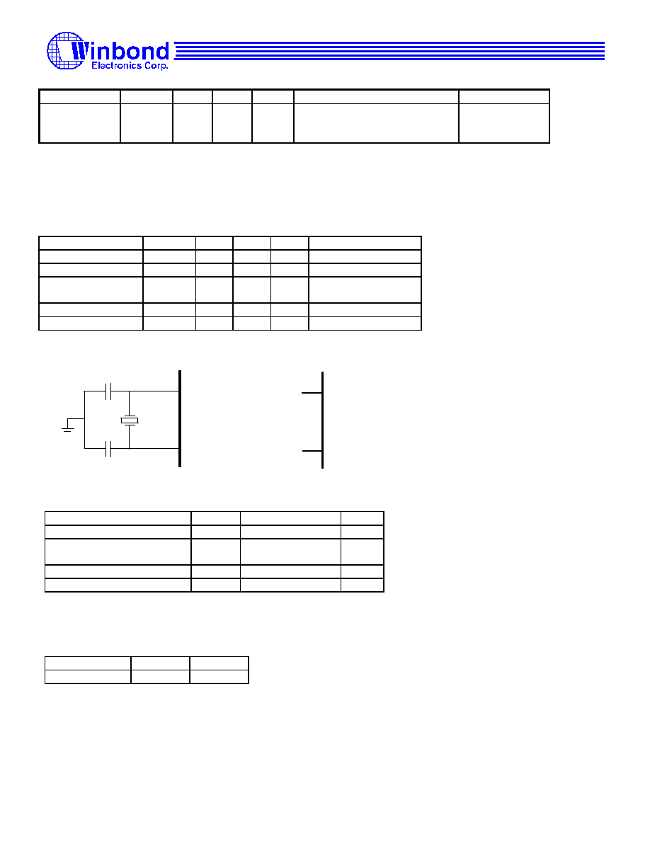
Preliminary Data Sheet
W6692 PCI ISDN S/T-Controller
Publication Release Date: Sep 30, 1999
Revision 0.9
-95 -
output current
Transmitter
output
impedence
R
X
30
23
k
Inactive or during binary ONE
During binary ZERO (R
L
=50
)
SX1,2
Note:
1)
Due to the transformer, the load resistance seen by the circuit is four times R
L
.
Capacitances
T
A
=25
�
C, V
DD
= 5 V
�
5 %, V
SSA
= 0V, V
SSD
=0V, fc=1 Mhz, unmeasured pins grounded.
Parameter
Symbol
Min.
Max.
Unit Remarks
Input capacitance
C
IN
7
pF
All pins except SR1,2
I/O pin capacitance
C
IO
7
pF
All pins except SR1,2
Output capacitance
against V
SSA
C
OUT
10
pF
SX1,2
Input capacitance
C
IN
7
pF
SR1,2
Load capacitance
C
L
50
pF
XTAL1,2
Recommended oscillator circuits
Crystal specifications
Parameter
Symbol Values
Unit
Frequency
f
7.680
MHz
Frequency calibration
tolerance
Max. 100
ppm
Load capacitance
C
L
Max. 50
pF
Oscillator mode
Fundamental
Note: The load capacitance C
L
depends on the crystal specification. The typical values are 33 to 47 pF.
External ocsillator input (XTAL1) clock characteristics
Parameter
Min.
Max.
Duty cycle
1:2
2:1
50
XTAL1
XTAL2
51
7.68MHz
C
L
50pF
C
L
C
L
50
XTAL1
XTAL2
51
External
oscillator
signal
N.C.
or
Preliminary Data Sheet
W6692 PCI ISDN S/T-Controller
Publication Release Date: Sep 30, 1999
Revision 0.9
-96 -
9.4 Preliminary Switching Characteristics
9.4.1 PCM Interface Timing
1)
Note 1: These drawings are not to scale.
Note 2: The frequency of PBCK is 1536 kHz which includes 24 channels of 64 kbps data. The PFCK1 and PFCK2 are located at
channel 1 and channel 13, each with a 8 x PBCK duration.
Detailed PCM timing
PBCK
PFCK1
PFCK2
PTXD
PRXD
ta1
ta2
ta3
ta4
ta5
ta6
ta7
ta8
PBCK
2)
(1.536MHz)
PFCK1
2)
PFCK2
2)
PTXD
PRXD
24 CHs
CH 1
CH 13
Port1
Port1
Port2
Port2
Port1
Port1

Preliminary Data Sheet
W6692 PCI ISDN S/T-Controller
Publication Release Date: Sep 30, 1999
Revision 0.9
-97 -
Parameter
Parameter Descriptions
Min.
Max.
Remarks
ta1
PBCK pulse high
260
Unit = ns
ta2
PBCK pulse low
260
ta3
Frame clock asserted from
PBCK
20
ta4
PTXD data delay from PBCK
20
ta5
Frame clock deasserted from
PBCK
20
ta6
PTXD hold time from PBCK
10
ta7
PRXD setup time to PBCK
20
ta8
PRXD hold time from PBCK
10
9.4.2 Serial EEPROM Timing
Parameter Parameter Descriptions
Min.
Max.
Remarks
tb1
EPSK low
2500
Unit = ns
tb2
EPSK high
2500
tb3
EPCS output delay
30
tb4
EPSD output delay
30
tb5
EPSD tri-state delay
30
tb6
EPSD input setup time
30
tb7
EPSD input hold time
30
9.4.3 Peripheral Interface Timing
8-bit microprocessor timing when XMODE = 1:
A5
A4
A1
A0
.....
D15
D14
D1
D0
.......
tb1
tb2
tb3
tb3
tb4
tb4
tb5
tb7
tb6
EPSK
EPCS
EPSDI
Preliminary Data Sheet
W6692 PCI ISDN S/T-Controller
Publication Release Date: Sep 30, 1999
Revision 0.9
-98 -
XALE
PCI CLK
XAD7-0
XWRB
Peripheral Write
tc1
tc2
tc3
tc5
tc4
Hi-Z
Hi-Z
Hi-Z
Hi-Z
Hi-Z
Hi-Z
XALE
PCI CLK
XAD7-0
XRDB
Peripheral Read
tc1
tc2
tc7
tc8
tc6
Hi-Z
Hi-Z
Hi-Z
Hi-Z
Hi-Z
Hi-Z
Parameter Parameter Descriptions
Min.
Max.
Typical
Remarks
tc1
XA7-0 setup time
30
Unit = ns
tc2
XA7-0 hold time
30
tc3
XWRB pulse width
60
tc4
write data setup time
90
tc5
write data hold time
30
tc6
XRDB pulse width
120
tc7
read data delay time
90
tc8
read data hold time
0
9.4.5 8-bit Microprocessor Timing
Intel mode read cycle timing
t1
ALE
t3
t11
t5
t10
AD<7:0>
RD#
CS#
t8
t2
A<7:0>
D<7:0>
A<7:0>
t4
t9
t6
t7
Preliminary Data Sheet
W6692 PCI ISDN S/T-Controller
Publication Release Date: Sep 30, 1999
Revision 0.9
-99 -
Intel mode write cycle timing
Motorola mode read cycle timing
t1
ALE
t3
t13
t12
t10
AD<7:0>
WR#
CS#
t14
t2
A<7:0>
D<7:0>
A<7:0>
t4
t15
t6
t7
A<7:0>
t21
CS#
RW
DS#
t19
t16
t18
t24
t20
t23
D<7:0>
t22
t17
Preliminary Data Sheet
W6692 PCI ISDN S/T-Controller
Publication Release Date: Sep 30, 1999
Revision 0.9
-100
-
Motorola mode write cycle timing
Parameter Parameter Descriptions
Min.
Max.
Remarks
t1
ALE pulse width
50
t2
address setup time to ALE
15
t3
address hold time from ALE
10
t4
address setup time to RD#, WR#
0
t5
RD# pulse width
110
t6
CS# setup time to RD#, WR#
0
t7
CS# hold time from RD#, WR#
0
t8
data output delay from RD#
50
t9
data float from RD#
25
t10
ALE guard time
15
t11
RD# recovery time
70
t12
WR# pulse width
60
t13
WR# recovery time
70
t14
data setup time to WR#
35
t15
data hold time from WR#
10
t16
address setup time to DS#
25
t17
address hold time from DS#
10
t18
CS# setup time to DS#
10
t19
CS# hold time from DS#
10
t20
DS# read pulse width
110
t21
DS# read recovery time
70
t22
RW setup time to DS# read
0
t23
data output delay from DS#
110
t24
data hold time from DS#
25
t25
RW setup time to DS# write
0
t26
DS# write pulse width
60
t27
DS# write recovery time
70
t28
write data setup time to DS#
35
t29
write data hold time from DS#
10
A<7:0>
t27
CS#
RW
DS#
t19
t16
t18
t29
t26
t28
D<7:0>
t25
t17

Preliminary Data Sheet
W6692 PCI ISDN S/T-Controller
Publication Release Date: Sep 30, 1999
Revision 0.9
-101
-
9.5 AC Timing Test Conditions
T
A
= 0 to 70
�
C, V
DD
= 5 V
�
5 %
Inputs are driven to 2.4 V for logical 1 and 0.4 V for logical 0. Measurements are made at 2.0 V for logical 1 and 0.8 V for
logical 0. The AC testing input/output waveforms are shown below :
". "0".

Preliminary Data Sheet
W6692 PCI ISDN S/T-Controller
Publication Release Date: Sep 30, 1999
Revision 0.9
-102
-
10. PACKAGE SPECIFICATIONS
100L QFP(14x20x2.75mm footprint 4.8mm)
Preliminary Data Sheet
W6692 PCI ISDN S/T-Controller
Publication Release Date: Sep 30, 1999
Revision 0.9
-103
-
E
H
y
A
A2
Seating Plane
L
L
1
See Detail F
0.08
0
7
0
0.003
2.40
1.40
19.20
1.20
18.80
1.00
18.40
0.064
0.055
0.992
0.756
0.047
0.976
0.740
0.039
0.960
0.746
0.65
20.10
14.10
0.20
0.40
2.87
20.00
14.00
2.72
19.90
13.90
0.10
0.20
2.57
0.791
0.555
0.008
0.016
0.113
0.787
0.551
0.107
0.026
0.783
0.547
0.004
0.008
0.101
Symbol
Min
Nom
Max
Max
Nom
Min
Dimension in inch
Dimension in mm
A
b
c
D
e
H
D
H
E
L
y
A
A
L
1
1
2
E
0.012
0.006
0.15
0.30
24.40
24.80
25.20
7
0.020
0.032
0.498
0.802
0.35
0.25
0.010
0.014
0.018
0.45
Controlling dimension : Millimeters
Controlling dimension : Millimeters
A1
E
D
H
D
e
e
b
b
c
c

Preliminary Data Sheet
W6692 PCI ISDN S/T-Controller
Publication Release Date: Sep 30, 1999
Revision 0.9
-104
-
Headquarters
No. 4, Creation Rd. III
Science-Based Industrial Park
Hsinchu, Taiwan
TEL: 886-35-770066
FAX: 886-35-789467
www: http://www.winbond.com.tw/
Taipei Office
11F, No. 115, Sec. 3, Min-Sheng East Rd.
Taipei, Taiwan
TEL: 886-2-7190505
FAX: 886-2-7197502
TLX: 16485 WINTPE
Winbond Electronics (H.K.) Ltd.
Rm. 803, World Trade Square, Tower II
123 Hoi Bun Rd., Kwun Tong
Kowloon, Hong Kong
TEL: 852-27516023-7
FAX: 852-27552064
Winbond Electronics
(North America) Corp.
2730 Orchard Parkway
San Jose, CA 95134 U.S.A.
TEL: 1-408-9436666
FAX: 1-408-9436668
Note: All data and specifications are subject to change without notice.