 | –≠–ª–µ–∫—Ç—Ä–æ–Ω–Ω—ã–π –∫–æ–º–ø–æ–Ω–µ–Ω—Ç: W6811I | –°–∫–∞—á–∞—Ç—å:  PDF PDF  ZIP ZIP |

Publication Release Date: October 10, 2002
- 1 -
Revision A9
W6811
SINGLE-CHANNEL VOICEBAND CODEC
(5V Analog, 3V Digital)
Preliminary Data Sheet

W6811
- 2 -
1. GENERAL DESCRIPTION
The W6811 is a general-purpose single channel PCM CODEC with pin-selectable
µ-Law or A-Law
companding. The device is compliant with the ITU G.712 specification. It operates off of a separated
analog (5V) and digital (3V) power supplies and is available in 24-pin PDIP, SOG, SSOP, and TSSOP
package options. Functions performed include digitization and reconstruction of voice signals, and
band limiting and smoothing filters required for PCM systems. The filters are compliant with ITU G.712
specification. W6811 performance is specified over the industrial temperature range of ≠40
∞C to
+85
∞C.
The W6811 includes an on-chip precision voltage reference and an additional power amplifier,
capable of driving 300
loads differentially up to a level of 6.3V peak-to-peak. The analog section is
fully differential, reducing noise and improving the power supply rejection ratio. The data transfer
protocol supports both long-frame and short-frame synchronous communications for PCM
applications, and IDL and GCI communications for ISDN applications. W6811 accepts seven master
clock rates between 256 kHz and 4.096 MHz, and an on-chip pre-scaler automatically determines the
division ratio for the required internal clock.
2. FEATURES
∑ Power supply:
Analog 4.5 ≠ 5.5V
Digital 2.7 ≠ 3.3V
∑ Typical power dissipation of 25 mW,
power-down mode of 0.5
µW
∑ Fully-differential analog circuit design
∑ On-chip precision reference of 1.575 V for
a 0 dBm TLP at 600
∑ Push-pull power amplifiers with external
gain adjustment with 300
load capability
∑ Seven master clock rates of 256 kHz to
4.096 MHz
∑ Pin-selectable
µ-Law and A-Law
companding (compliant with ITU G.711)
∑ CODEC A/D and D/A filtering compliant
with ITU G.712
∑ Industrial temperature range (≠40∞C to
+85
∞C)
∑ Four packages: 24-pin PDIP, SOG, SSOP,
and TSSOP
APPLICATIONS
∑ Digital Telephone Systems
∑ Central Office Equipment (Gateways,
Switches, Routers)
∑ PBX Systems (Gateways, Switches)
∑ PABX/SOHO Systems
∑ Local Loop card
∑ SOHO Routers
∑ VoIP Terminals
∑ Enterprise Phones
∑ ISDN Terminals
∑ Analog line cards
∑ Digital Voice Recorders
W6811
Publication Release Date: October 10, 2002
- 3 -
Revision A9
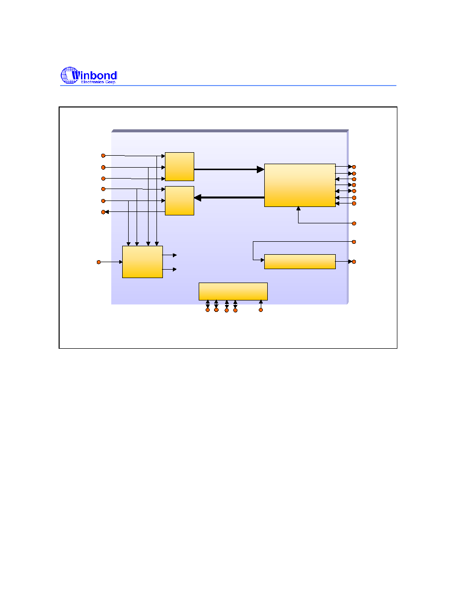
3. BLOCK DIAGRAM
256 kHz,
512 kHz,
1536 kHz,
1544 kHz,
2048 kHz,
2560 kHz
& 4096 kHz
MCLK
256 kHz
8 kHz
512 kHz
Pre - scaler
V
DD
A
V
SSA
Power Conditioning
Voltage reference
V
AG
PU
I
G.712 CODEC
G.711
µ
/A -Law
PAO+
PAO-
PAI
RO
-
AO
AI+
AI-
µ
/A-Law
Tra
ns
mit
PC
M
Int
erf
ace
Re
cei
ve
PC
M
Int
erf
ace
FST
BCLKT
PCMT
FSR
BCLKR
PCMR
V
REF
256 kHz,
512 kHz,
1536 kHz,
1544 kHz,
2048 kHz,
2560 kHz
& 4096 kHz
MCLK
256 kHz
8 kHz
Pre - Saler
Power Conditioning
Voltage reference
V
AG
G.712 CODEC
G.711
µ
/A -Law
RO
µ
/A-Law
G.712 CODEC
G.711
µ
/A -Law
RO
µ
/A-Law
Tr
ansmit
PCM
Inte
rfa
ce
R
e
ce
i
v
e
PCM
Inte
rfa
ce
BCLKT
BCLKT
BCLKR
V
V
DDD
V
SSD

W6811
- 4 -
4. TABLE OF CONTENTS
1. GENERAL DESCRIPTION ................................................................................................................. 2
2. FEATURES ......................................................................................................................................... 2
3. BLOCK DIAGRAM .............................................................................................................................. 3
4. TABLE OF CONTENTS ...................................................................................................................... 4
5. PIN CONFIGURATION ....................................................................................................................... 6
6. PIN DESCRIPTION............................................................................................................................. 7
7. FUNCTIONAL DESCRIPTION............................................................................................................ 9
7.1. Transmit Path............................................................................................................................. 9
7.2. Receive Path............................................................................................................................ 10
7.3. Power Management................................................................................................................. 11
7.3.1. Analog Supply ................................................................................................................ 11
7.3.2. Digital Supply ................................................................................................................. 11
7.3.3. Analog Ground Reference Bypass................................................................................. 11
7.3.4. Analog Ground Reference Voltage Output .................................................................... 11
7.4. PCM Interface .......................................................................................................................... 11
7.4.1. Long Frame Sync ........................................................................................................... 12
7.4.2. Short Frame Sync .......................................................................................................... 12
7.4.3. GCI Interface .................................................................................................................. 12
7.4.4. IDL Interface................................................................................................................... 13
7.4.5. System Timing................................................................................................................ 13
8. TIMING DIAGRAMS.......................................................................................................................... 14
9. ABSOLUTE MAXIMUM RATINGS.................................................................................................... 21
9.1. Absolute Maximum Ratings ................................................................................................... 21
9.2. Operating Conditions ............................................................................................................. 21
10. ELECTRICAL CHARACTERISTICS ............................................................................................... 22
10.1. General Parameters .............................................................................................................. 22
10.2. Analog Signal Level and Gain Parameters............................................................................ 23
10.3. Analog Distortion and Noise Parameters .............................................................................. 24
10.4. Analog Input and Output Amplifier Parameters ..................................................................... 25
10.5. Digital I/O ............................................................................................................................... 27
10.5.1. µ-Law Encode Decode Characteristics........................................................................ 27
10.5.2. A-Law Encode Decode Characteristics ....................................................................... 28
10.5.3. PCM Codes for Zero and Full Scale ............................................................................ 29
10.5.4. PCM Codes for 0dBm0 Output .................................................................................... 29
11. TYPICAL APPLICATION CIRCUIT................................................................................................. 30

W6811
Publication Release Date: October 10, 2002
- 5 -
Revision A9
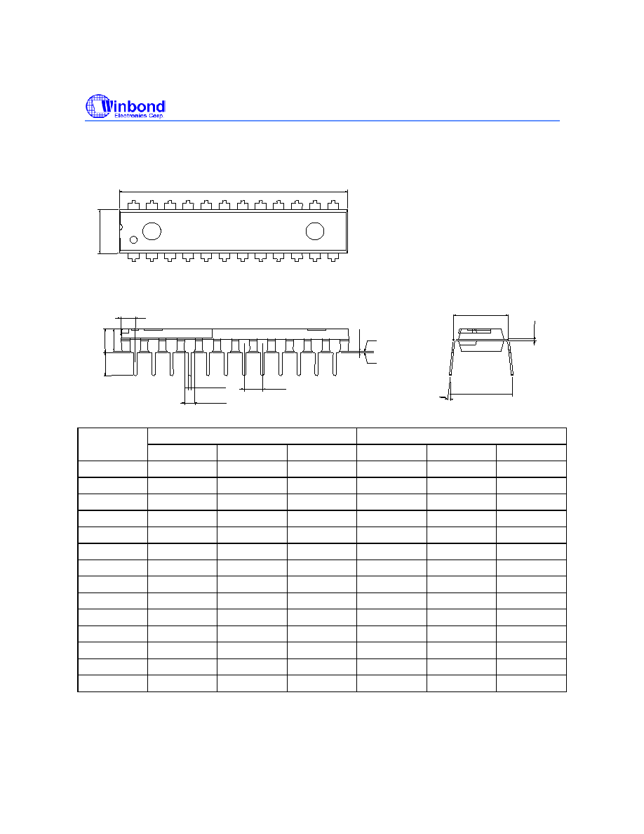
12. PACKAGE SPECIFICATION .......................................................................................................... 32
12.1. 24L TSSOP ≠ 4.4X7.8mm ..................................................................................................... 32
12.2. 24L SOP ≠ 300mil.................................................................................................................. 33
12.3. 24L SSOP ≠ 150mil ............................................................................................................... 34
12.4. 24L PDIP ≠ 300 mil ................................................................................................................ 35
13. ORDERING INFORMATION........................................................................................................... 36
14. VERSION HISTORY ....................................................................................................................... 37
W6811
- 6 -
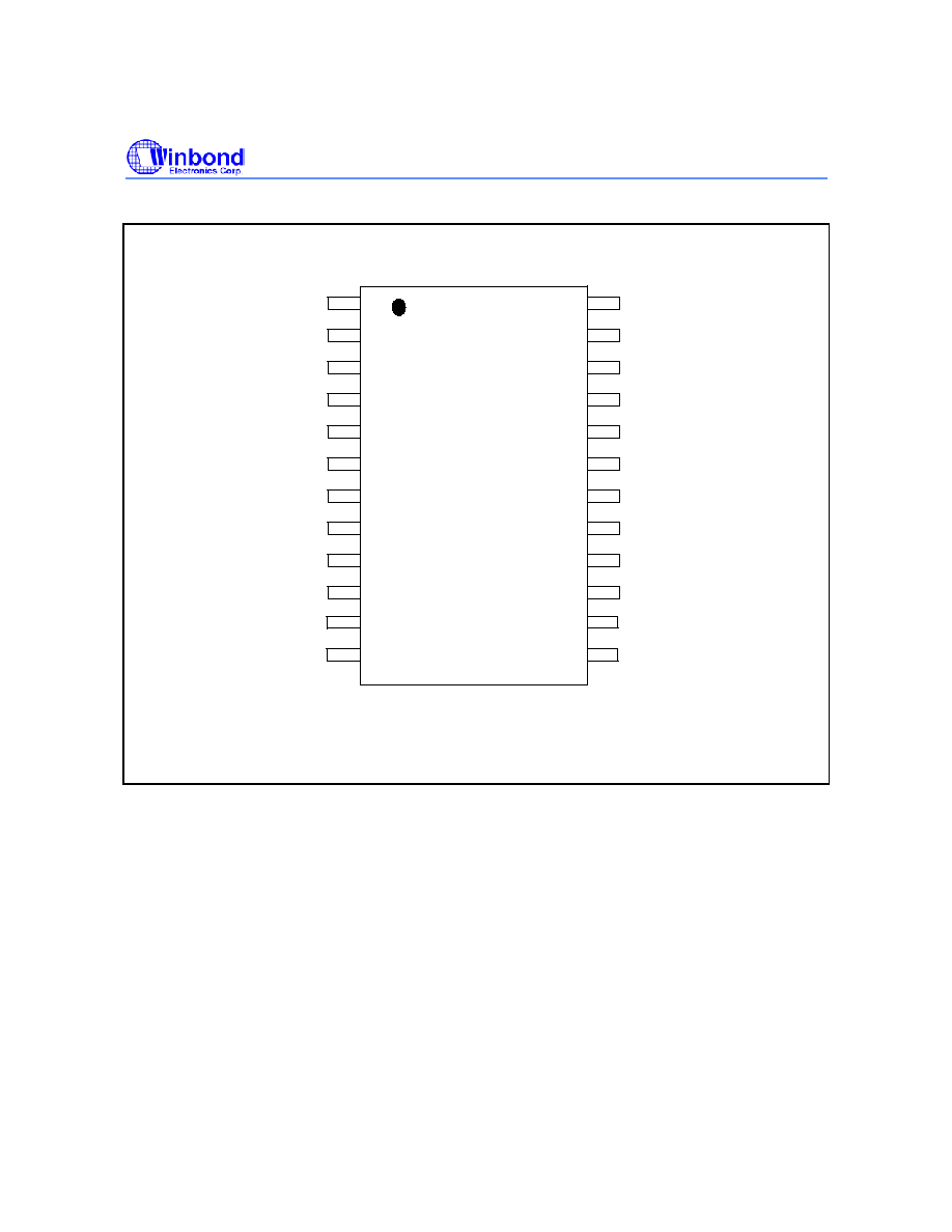
5. PIN CONFIGURATION
PDIP/SOP/SSOP/TSSOP
V
AG
AI+
AI-
AO
µ/A-Law
V
SSA
FST
PCMT
BCLKT
MCLK
V
SSD
NC
V
REF
RO
-
PAI
PAO
-
PAO+
V
DDA
FSR
PCMI
BCLKR
PUI
V
DDD
NC
V
AG
AI+
AI-
AO
V
SSA
MCLK
V
SSD
NC
V
REF
RO
-
PAI
PAO
-
PAO+
V
DDA
FSR
PCMR
BCLKR
PUI
V
DDD
NC
V
AG
24
AI+ 23
AI-
22
AO 21
µ
/A 20
V
SSA
19
FSX 16
PCMO 15
BCLKT 14
MCLK 13
1 V
REF
2 RO-
3 PAI
4 PAO -
5 PAO+
6 V
DDA
9 FSR
10 PCMI
11 BCLKR
12 PUI
V
SSD
17
8 V
DDD
NC 18
7 NC
24
23
22
21
20
19
16
15
14
13
1
2
3
4
5
6
9
10
11
12
17
8
18
7
W6811
Publication Release Date: October 10, 2002
- 7 -
Revision A9
6. PIN DESCRIPTION
Pin
Name
Pin
No.
V
DD
*
Functionality
V
REF
1
A
This pin is used to bypass the on-chip 2.5V voltage reference. It needs to be
decoupled to V
SSA
through a 0.1
µF ceramic decoupling capacitor. No
external loads should be tied to this pin.
RO-
2
A
Inverting output of the receive smoothing filter. This pin can typically drive a 2
k
load to 1.575 volt peak referenced to the analog ground level.
PAI
3
A
This pin is the inverting input to the power amplifier. Its DC level is at the V
AG
voltage.
PAO- 4 A Inverting power amplifier output. This pin can drive a 300
load to 1.575 volt
peak referenced to the V
AG
voltage level.
PAO+ 5 A Non-inverting power amplifier output. This pin can drive a 300
load to 1.575
Volt peak referenced to the V
AG
voltage level.
V
DDA
6 A Analog power supply. This pin should be decoupled to V
SSA
with a 0.1
µF
ceramic capacitor.
NC 7
Not
Connected
V
DDD
8 D Digital power supply. This pin should be decoupled to V
SSD
with a 0.1
µF
ceramic capacitor. For correct operation, V
DDD
value should always be lower
then V
DDA
.
FSR
9
D
8 kHz Frame Sync input for the PCM receive section. This pin also selects
channel 0 or channel 1 in the GCI and IDL modes. It can also be connected
to the FST pin when transmit and receive are synchronous operations.
PCMR
10
D
PCM input data receive pin. The data needs to be synchronous with the FSR
and BCLKR pins.
BCLKR
11
D
PCM receive bit clock input pin. This pin also selects the interface mode. The
GCI mode is selected when this pin is tied to V
SSD
. The IDL mode is selected
when this pin is tied to V
DDD
. This pin can also be tied to the BCLKT when
transmit and receive are synchronous operations.
PUI
12
D
Power up input signal. When this pin is tied to V
DDD
, the part is powered up.
When tied to V
SSD
, the part is powered down.
MCLK
13
D
System master clock input. Possible input frequencies are 256 kHz, 512 kHz,
1536 kHz, 1544 kHz, 2048 kHz, 2560 kHz & 4096 kHz. For a better
performance, it is recommended to have the MCLK signal synchronous and
aligned to the FST signal. This is a requirement in the case of 256 and 512
kHz frequency.
BCLKT
14
D
PCM transmit bit clock input pin.
PCMT
15
D
PCM output data transmit pin. The output data is synchronous with the FST
and BCLKT pins.
FST
16
D
8 kHz transmit frame sync input. This pin synchronizes the transmit data
bytes.
W6811
- 8 -
Pin
Name
Pin
No.
V
DD
*
Functionality
V
SSD
17
D
This is the digital supply ground. This pin should be connected to 0V.
NC 18
Not
Connected
V
SSA
19
A
This is the analog supply ground. This pin should be connected to 0V.
µ/A-Law 20 D Compander mode select pin. µ-Law companding is selected when this pin is
tied to V
DDD
. A-Law companding is selected when this pin is tied to V
SSD
.
AO
21
A
Analog output of the first gain stage in the transmit path.
AI-
22
A
Inverting input of the first gain stage in the transmit path.
AI+
23
A
Non-inverting input of the first gain stage in the transmit path.
V
AG
24
A
Mid-Supply analog ground pin, which supplies a 2.5 Volt reference voltage for
all-analog signal processing. This pin should be decoupled to V
SSA
with a
0.01
µF capacitor. This pin becomes high impedance when the chip is
powered down.
* These columns represent whether the pin Is driven by Analog (`A') or Digital (`D') power supply.
W6811
Publication Release Date: October 10, 2002
- 9 -
Revision A9
7. FUNCTIONAL DESCRIPTION
W6811 is a single-rail, single channel PCM CODEC for voiceband applications. The CODEC complies
with the specifications of the ITU-T G.712 recommendation. The CODEC also includes a complete
µ-
Law and A-Law compander. The
µ-Law and A-Law companders are designed to comply with the
specifications of the ITU-T G.711 recommendation.
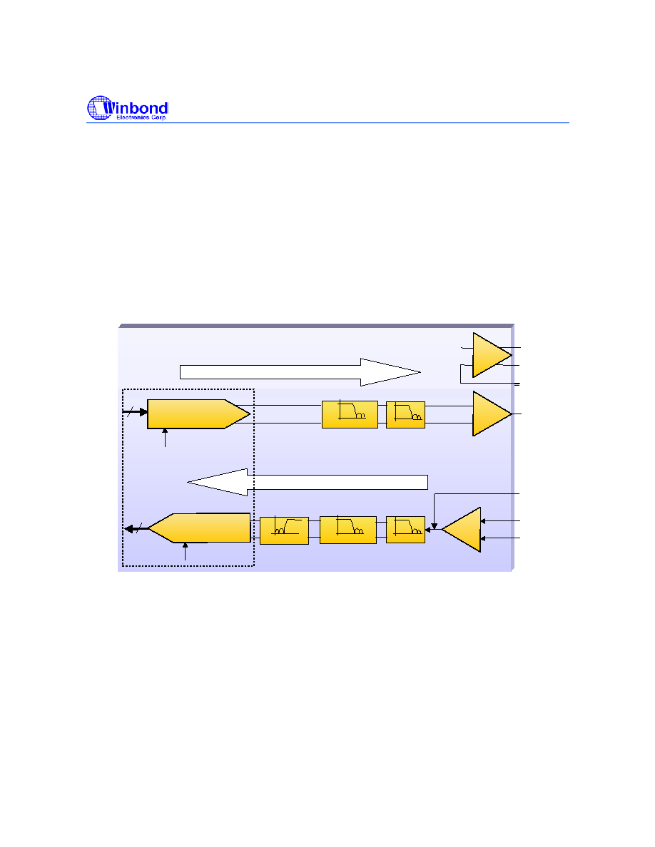
The block diagram in section 3 shows the main components of the W6811. The chip consists of a
PCM interface, which can process long and short frame sync formats, as well as GCI and IDL formats.
The pre-scaler of the chip provides the internal clock signals and synchronizes the CODEC sample
rate with the external frame sync frequency. The power conditioning block provides the internal power
supply for the digital and the analog section, while the voltage reference block provides a precision
analog ground voltage for the analog signal processing. The main CODEC block diagram is shown in
section 3.
Figure 7.1 The W6811 Signal Path
7.1. T
RANSMIT
P
ATH
The A-to-D path of the CODEC contains an analog input amplifier with externally configurable gain
setting (see application examples in section 11). The device has an input operational amplifier whose
output is the input to the encoder section. If the input amplifier is not required for operation it can be
powered down and bypassed. In that case a single ended input signal can be applied to the AO pin or
the AI- pin. The AO pin becomes high input impedance when the input amplifier is powered down. The
input amplifier can be powered down by connecting the AI+ pin to V
DDA
or V
SSA
. The AO pin is
selected as an input when AI+ is tied to V
DDA
and the AI- pin is selected as an input when AI+ is tied to
V
SSA
(see Table 7.1).
PAO+
PAO
8
µ/A
-
Cont
AI+
AI -
w
µ/A-
Cont
ol
AO
+
RO-
-
VA
G
Ant-Aliasi
Filter
=
H
Ant
i
-Aliasi
n
Filter
f
C
= 200
H
High
Pas
Filt
Smoot
nFilter
2
H
Smoot
nFilter
1
8
µ/A
Control
8
µ/A-
Control
PAI
V
AG
Ant-Aliasing
Filter
-
Aliasing
Filter
Ant-
Filter
High Pass
Filter
Smoothing
Filter
Filter
Smoothing
Filter
Filter
Receive Path
Transmit Path
+ -
+
+
+
-
A/D
Converter
D/A
Converter
f
C
= 3400Hz
f
C
= 3400Hz
C
= 200Hz
f

W6811
- 10 -
AI+
Input Amplifier
Input
V
DDA
Powered
Down
AO
1.2 to V
DDA
-1.2
Powered Up
AI+, AI-
V
SSA
Powered
Down
AI-
Table 7.1 Input Amplifier Modes of operation
When the input amplifier is powered down, the input signal at AO or AI- needs to be referenced to the
analog ground voltage V
AG
.
The output of the input amplifier is fed through a low-pass filter to prevent aliasing at the switched
capacitor 3.4 kHz low pass filter. The 3.4 kHz switched capacitor low pass filter prevents aliasing of
input signals above 4 kHz, due to the sampling at 8 kHz. The output of the 3.4 kHz low pass filter is
filtered by a high pass filter with a 200 Hz cut-off frequency. The filters are designed according to the
recommendations in the G.712 ITU-T specification. From the output of the high pass filter the signal is
digitized. The signal is converted into a compressed 8-bit digital representation with either
µ-Law or A-
Law format. The
µ-Law or A-Law format is pin-selectable through the µ/A-Law pin. The compression
format can be selected according to Table 7.2.
µ/A-Law Pin
Format
V
SSA
A-Law
V
DDA
µ-Law
Table 7.2. Pin-selectable Compression Format
The digital 8-bit
µ-Law or A-Law samples are fed to the PCM interface for serial transmission at the
sample rate supplied by the external frame sync FST.
7.2. R
ECEIVE
P
ATH
The 8-bit digital input samples for the D-to-A path are serially shifted in by the PCM interface and
converted to parallel data bits. During every cycle of the frame sync FSR, the parallel data bits are fed
through the pin-selectable
µ-Law or A-Law expander and converted to analog samples. The mode of
expansion is selected by the
µ/A-Law pin as shown in Table 7.2. The analog samples are filtered by a
low-pass smoothing filter with a 3.4 kHz cut-off frequency, according to the ITU-T G.712 specification.
A sin(x)/x compensation is integrated with the low pass smoothing filter. The output of this filter is
buffered to provide the receive output signal RO-. The RO- output can be externally connected to the
PAI pin to provide a differential output with high driving capability at the PAO+ and PAO- pins. By
using external resistors (see section 11 for examples), various gain settings of this output amplifier
can be achieved. If the transmit power amplifier is not in use, it can be powered down by connecting
PAI to V
DDA
.
W6811
Publication Release Date: October 10, 2002
- 11 -
Revision A9
7.3. P
OWER
M
ANAGEMENT
7.3.1. Analog Supply
The power supply for the analog part of the W6811 needs to be 5V +/- 10%. This supply voltage is
connected to the V
DDA
pin. The V
DDA
pin needs to be decoupled to ground through a 0.1
µF ceramic
capacitor.
7.3.2. Digital Supply
The power supply for the digital part of the W6811 needs to be 3V +/- 10%. This supply voltage is
connected to the V
DDD
pin. The V
DDD
pin needs to be decoupled to ground through a 0.1
µF ceramic
capacitor.
7.3.3. Analog Ground Reference Bypass
The system has an internal precision voltage reference which generates the 2.5V mid-supply analog
ground voltage. This voltage needs to be decoupled to V
SSA
at the V
REF
pin through a 0.1
µF ceramic
capacitor.
7.3.4. Analog Ground Reference Voltage Output
The analog ground reference voltage is available for external reference at the V
AG
pin. This voltage
needs to be decoupled to V
SSA
through a 0.01
µF ceramic capacitor. The analog ground reference
voltage is generated from the voltage on the V
REF
pin and is also used for the internal signal
processing.
7.4. PCM I
NTERFACE
The PCM interface is controlled by pins BCLKR, FSR, BCLKT & FST. The input data is received
through the PCMR pin and the output data is transmitted through the PCMT pin. The modes of
operation of the interface are shown in Table 7.3.
BCLKR
FSR
Interface Mode
64 kHz to 4.096
MHz
8 kHz
Long or Short Frame Sync
V
SSD
V
SSD
ISDN GCI with active channel B1
V
SSD
V
DDD
ISDN GCI with active channel B2
V
DDD
V
SSD
ISDN IDL with active channel B1
V
DDD
V
DDD
ISDN IDL with active channel B2
Table 7.3 PCM Interface mode selections

W6811
- 12 -
7.4.1. Long Frame Sync
The Long Frame Sync or Short Frame Sync interface mode can be selected by connecting the
BCLKR or BCLKT pin to a 64 kHz to 4.096 MHz clock and connecting the FSR or FST pin to the 8
kHz frame sync. The device synchronizes the data word for the PCM interface and the CODEC
sample rate on the positive edge of the Frame Sync signal. It recognizes a Long Frame Sync when
the FST pin is held high for two consecutive falling edges of the bit-clock at the BCLKT pin. The length
of the Frame Sync pulse can vary from frame to frame, as long as the positive frame sync edge
occurs every 125
µsec. During data transmission in the Long Frame Sync mode, the transmit data pin
PCMT will become low impedance when the Frame Sync signal FST is high or when the 8 bit data
word is being transmitted. The transmit data pin PCMT will become high impedance when the Frame
Sync signal FST becomes low while the data is transmitted or when half of the LSB is transmitted. The
internal decision logic will determine whether the next frame sync is a long or a short frame sync,
based on the previous frame sync pulse. To avoid bus collisions, the PCMT pin will be high
impedance for two frame sync cycles after every power down state. More detailed timing information
can be found in the interface timing section.
7.4.2. Short Frame Sync
The W6811 operates in the Short Frame Sync Mode when the Frame Sync signal at pin FST is high
for one and only one falling edge of the bit-clock at the BCLKT pin. On the following rising edge of the
bit-clock, the W6811 starts clocking out the data on the PCMT pin, which will also change from high to
low impedance state. The data transmit pin PCMT will go back to the high impedance state halfway
the LSB. The Short Frame Sync operation of the W6811 is based on an 8-bit data word. When
receiving data on the PCMR pin, the data is clocked in on the first falling edge after the falling edge
that coincides with the Frame Sync signal. The internal decision logic will determine whether the next
frame sync is a long or a short frame sync, based on the previous frame sync pulse. To avoid bus
collisions, the PCMT pin will be high impedance for two frame sync cycles after every power down
state. More detailed timing information can be found in the interface timing section.
7.4.3. General Circuit Interface (GCI)
The GCI interface mode is selected when the BCLKR pin is connected to V
SSD
for two or more frame
sync cycles. It can be used as a 2B+D timing interface in an ISDN application. The GCI interface
consists of 4 pins : FSC (FST), DCL (BCLKT), Dout (PCMT) & Din (PCMR). The FSR pin selects
channel B1 or B2 for transmit and receive. Data transitions occur on the positive edges of the data
clock DCL. The Frame Sync positive edge is aligned with the positive edge of the data clock DCLK.
The data rate is running half the speed of the bit-clock. The channels B1 and B2 are transmitted
consecutively. Therefore, channel B1 is transmitted on the first 16 clock cycles of DCL and B2 is
transmitted on the second 16 clock cycles of DCL. For more timing information, see the timing section.

W6811
Publication Release Date: October 10, 2002
- 13 -
Revision A9
7.4.4. Interchip Digital Link (IDL)
The IDL interface mode is selected when the BCLKR pin is connected to V
DDD
for two or more frame
sync cycles. It can be used as a 2B+D timing interface in an ISDN application. The IDL interface
consists of 4 pins : IDL SYNC (FST), IDL CLK (BCLKT), IDL TX (PCMT) & IDL RX (PCMR). The FSR
pin selects channel B1 or B2 for transmit and receive. The data for channel B1 is transmitted on the
first positive edge of the IDL CLK after the IDL SYNC pulse. The IDL SYNC pulse is one IDL CLK
cycle long. The data for channel B2 is transmitted on the eleventh positive edge of the IDL CLK after
the IDL SYNC pulse. The data for channel B1 is received on the first negative edge of the IDL CLK
after the IDL SYNC pulse. The data for channel B2 is received on the eleventh negative edge of the
IDL CLK after the IDL SYNC pulse. The transmit signal pin IDL TX becomes high impedance when
not used for data transmission and also in the time slot of the unused channel. For more timing
information, see the timing section.
7.4.5. System Timing
The system can work at 256 kHz, 512 kHz, 1536 kHz, 1544 kHz, 2048 kHz, 2560 kHz & 4096 kHz
master clock rates. The system clock is supplied through the master clock input MCLK and can be
derived from the bit-clock if desired. An internal pre-scaler is used to generate a fixed 256 kHz and 8
kHz sample clock for the internal CODEC. The pre-scaler measures the master clock frequency
versus the Frame Sync frequency and sets the division ratio accordingly. If the Frame Sync is low for
the entire frame sync period while the MCLK and BCLK pin clock signals are still present, the W6811
will enter the low power standby mode. Another way to power down is to set the PUI pin to low. When
the system needs to be powered up again, the PUI pin needs to be set to high and the Frame Sync
pulse needs to be present. It will take two Frame Sync cycles before the pin PCMT will become low
impedance.
W6811
- 14 -
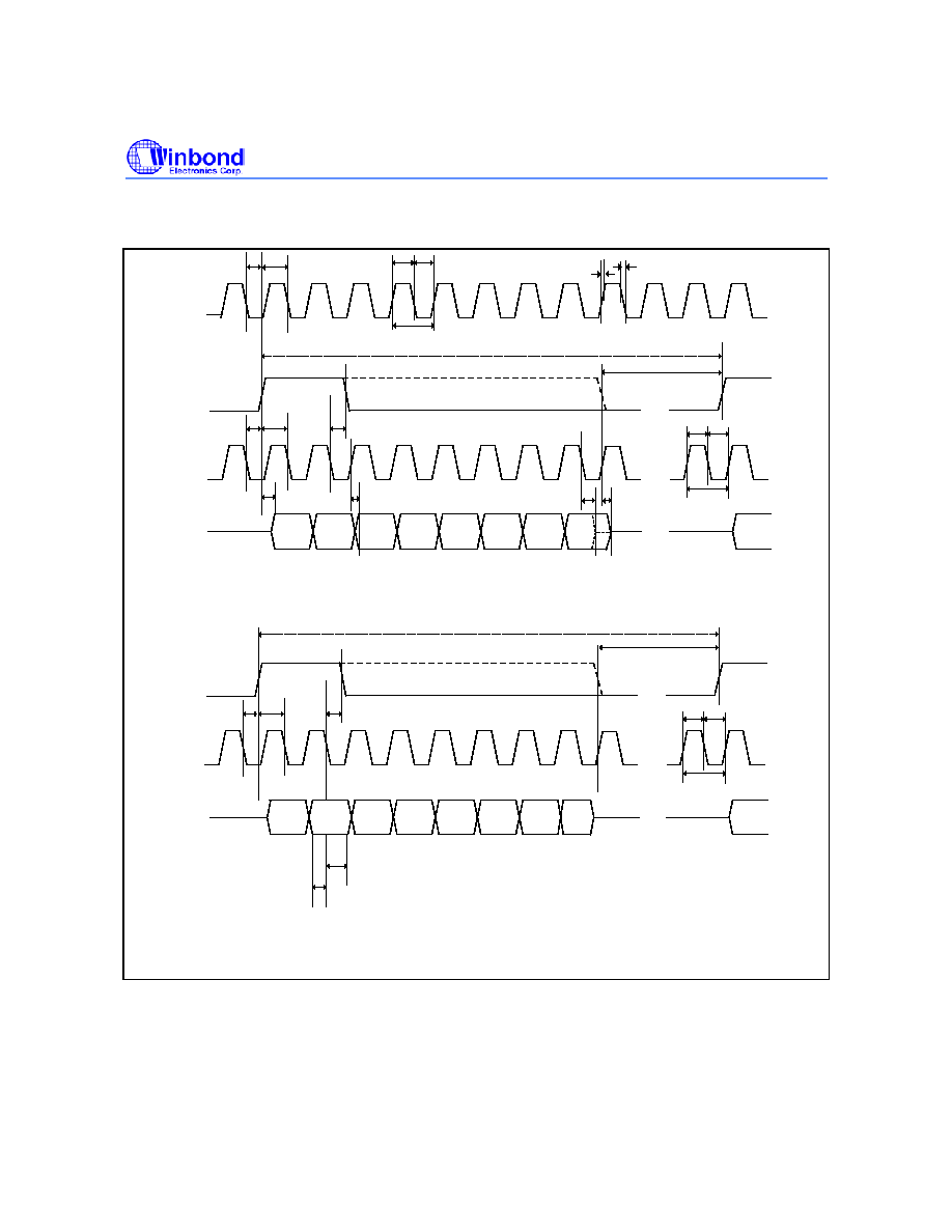
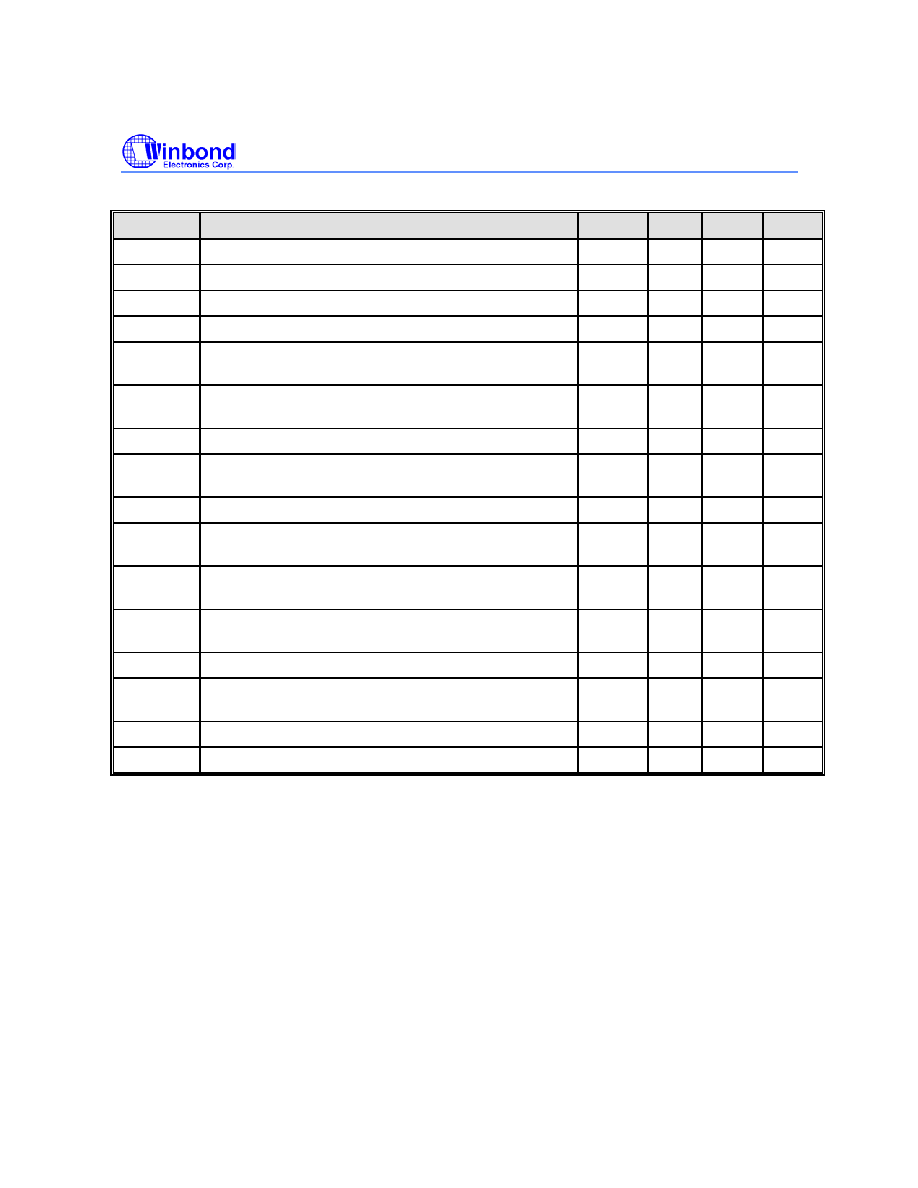
8. TIMING DIAGRAMS
Figure 8.1 Long Frame Sync PCM Timing
FST
B C L K T
D 7
D 6
D 5
D 4
D 3
D 2
D 1
PC M T
M SB
L SB
T
H ID
T
B C K
D 0
T
B C K H
T
B C K L
T
FS
T
FTFH
T
FTR S
T
FTR H
T
H ID
T
B D TD
T
FD TD
0
1
2
3
4
5
7
8
0
1
M SB
L SB
FSR
B C L K R
T
B C K
D 6
D 5
D 4
D 3
D 2
D 1 D 0
PC M R
D 7
T
D R H
T
D R S
T
B C K H
T
B C K L
T
FS
T
FR FH
T
FR R S
T
FR R H
0
1
2
3
4
5
6
7
8
0
1
6
M C L K
T
FTR H M
T
FTR SM
T
M C K H
T
M C K L
T
M C K
T
R ISE
T
FA L L
T
FSL
T
FSL
W6811
Publication Release Date: October 10, 2002
- 15 -
Revision A9
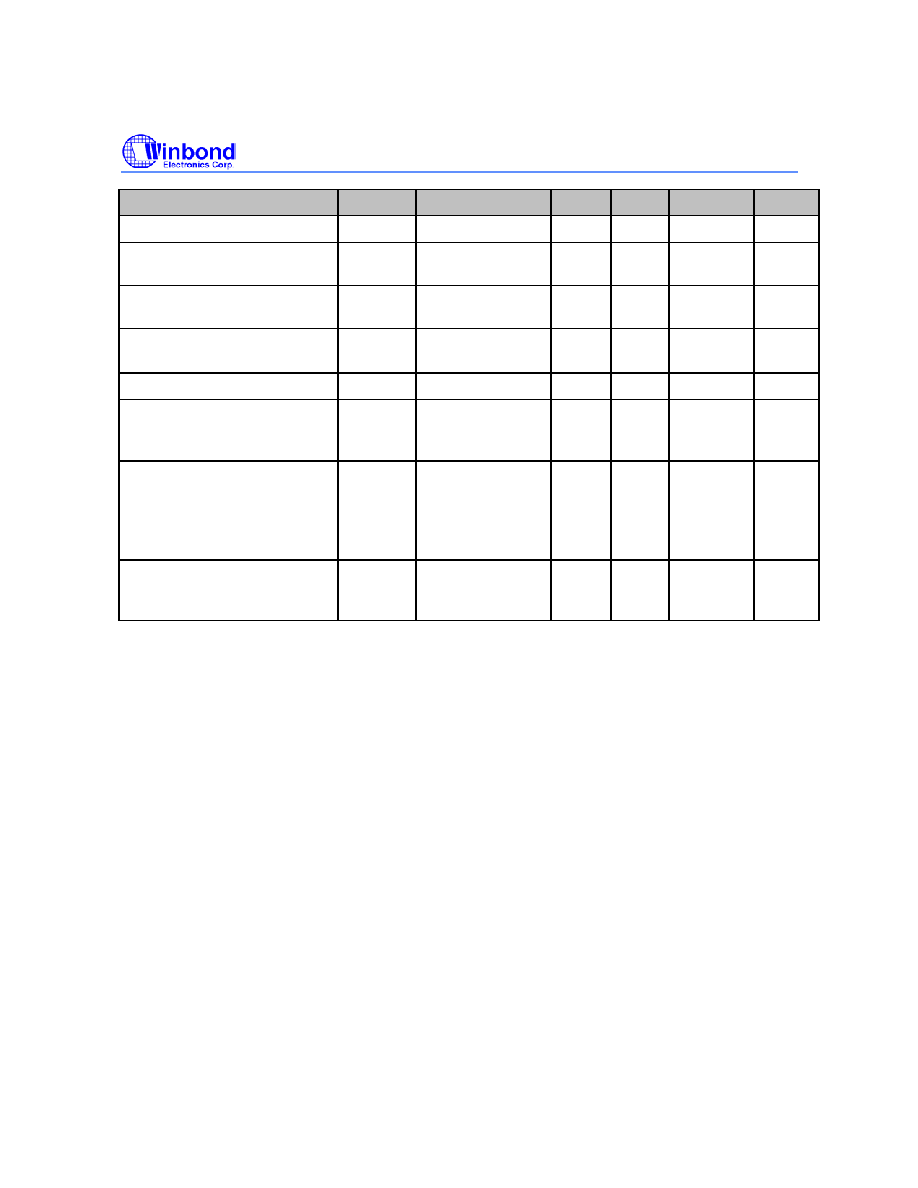
SYMBOL
DESCRIPTION
MIN
TYP
MAX
UNIT
1/T
FS
FST, FSR Frequency
---
8
---
kHz
T
FSL
FST / FSR Minimum Low Width
1
T
BCK
sec
1/T
BCK
BCLKT, BCLKR Frequency
64
---
4096
kHz
T
BCKH
BCLKT, BCLKR High Pulse Width
50
---
---
ns
T
BCKL
BCLKT, BCLKR Low Pulse Width
50
---
---
ns
T
FTRH
BCLKT 0 Falling Edge to FST Rising
Edge Hold Time
20 ---
---
ns
T
FTRS
FST Rising Edge to BCLKT 1 Falling
edge Setup Time
80 ---
---
ns
T
FTFH
BCLKT 2 Falling Edge to FST Falling
Edge Hold Time
50 ---
---
ns
T
FDTD
FST Rising Edge to Valid PCMT Delay
Time
--- ---
60
ns
T
BDTD
BCLKT Rising Edge to Valid PCMT
Delay Time
--- ---
60
ns
T
HID
Delay Time from the Later of FST
Falling Edge, or
BCLKT 8 Falling Edge to PCMT Output
High Impedance
10 ---
60
ns
T
FRRH
BCLKR 0 Falling Edge to FSR Rising
Edge Hold Time
20 ---
---
ns
T
FRRS
FSR Rising Edge to BCLKR 1 Falling
edge Setup Time
80 ---
---
ns
T
FRFH
BCLKR 2 Falling Edge to FSR Falling
Edge Hold Time
50 ---
---
ns
T
DRS
Valid PCMR to BCLKR Falling Edge
Setup Time
0 ---
---
ns
T
DRH
PCMR Hold Time from BCLKR Falling
Edge
50 ---
---
ns
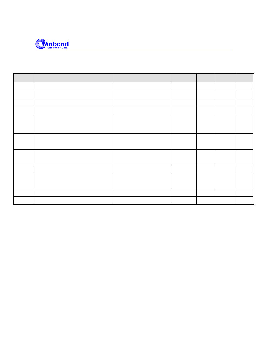
Table 8.1 Long Frame Sync PCM Timing Parameters
1
T
FSL
must be at least
T
BCK

W6811
- 16 -
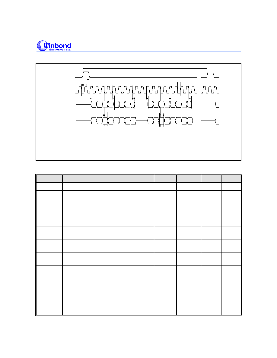
Figure 8.2 Short Frame Sync PCM Timing
D 7
D 6
D 5
D 4
D 3
D 2
D 1
M SB
L SB
T
B C K
D 0
T
B C K H
T
B C K L
T
FS
T
FTRS
T
FTRH
T
H ID
T
B D TD
0
1
2
3
4
5
6
7
8
0
1
FST
B C L K T
PC M T
T
B D TD
T
FTFH
-1
T
FTFS
M SB
L SB
T
B C K
D 6
D 5
D 4
D 3
D 2
D 1 D 0
D 7
T
D R H
T
D RS
T
B C K H
T
B C K L
T
FS
T
FR RS
T
FRR H
0
1
2
3
4
5
6
7
8
0
1
FSR
B C L K R
PC M R
T
FR FH
-1
T
FRFS
M C L K
T
FTR H M
T
FTR SM
T
M C K H
T
M C K L
T
M C K
T
R ISE
T
FA L L
W6811
Publication Release Date: October 10, 2002
- 17 -
Revision A9
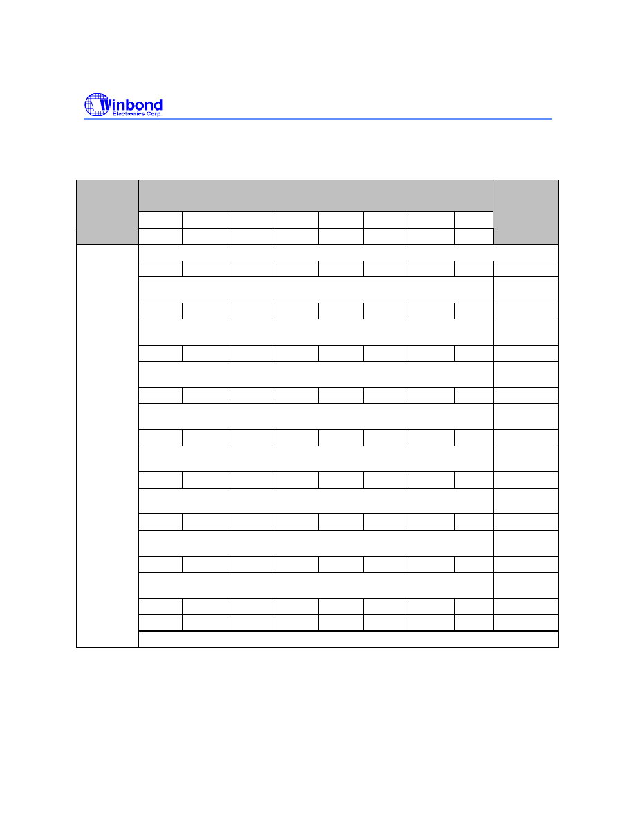
SYMBOL
DESCRIPTION
MIN
TYP
MAX
UNIT
1/T
FS
FST, FSR Frequency
---
8
---
kHz
1/T
BCK
BCLKT, BCLKR Frequency
64
---
4096
kHz
T
BCKH
BCLKT, BCLKR High Pulse Width
50
---
---
ns
T
BCKL
BCLKT, BCLKR Low Pulse Width
50
---
---
ns
T
FTRH
BCLKT ≠1 Falling Edge to FST Rising Edge Hold
Time
20 ---
--- ns
T
FTRS
FST Rising Edge to BCLKT 0 Falling edge Setup
Time
80 ---
--- ns
T
FTFH
BCLKT 0 Falling Edge to FST Falling Edge Hold Time 50
---
---
ns
T
FTFS
FST Falling Edge to BCLKT 1 Falling Edge Setup
Time
50 ---
--- ns
T
BDTD
BCLKT Rising Edge to Valid PCMT Delay Time
10
---
60
ns
T
HID
Delay Time from BCLKT 8 Falling Edge to PCMT
Output High Impedance
10 ---
60
ns
T
FRRH
BCLKR ≠1 Falling Edge to FSR Rising Edge Hold
Time
20 ---
--- ns
T
FRRS
FSR Rising Edge to BCLKR 0 Falling edge Setup
Time
80 ---
--- ns
T
FRFH
BCLKR 0 Falling Edge to FSR Falling Edge Hold Time 50
---
---
ns
T
FRFS
FSR Falling Edge to BCLKR 1 Falling Edge Setup
Time
50 ---
--- ns
T
DRS
Valid PCMR to BCLKR Falling Edge Setup Time
0
---
---
ns
T
DRH
PCMR Hold Time from BCLKR Falling Edge
50
---
---
ns
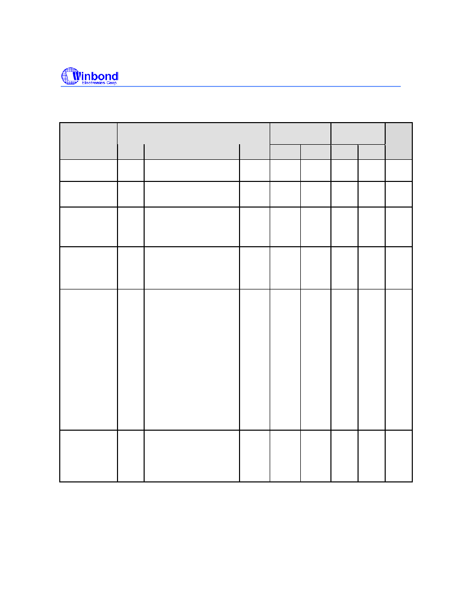
Table 8.2 Short Frame Sync PCM Timing Parameters
W6811
- 18 -
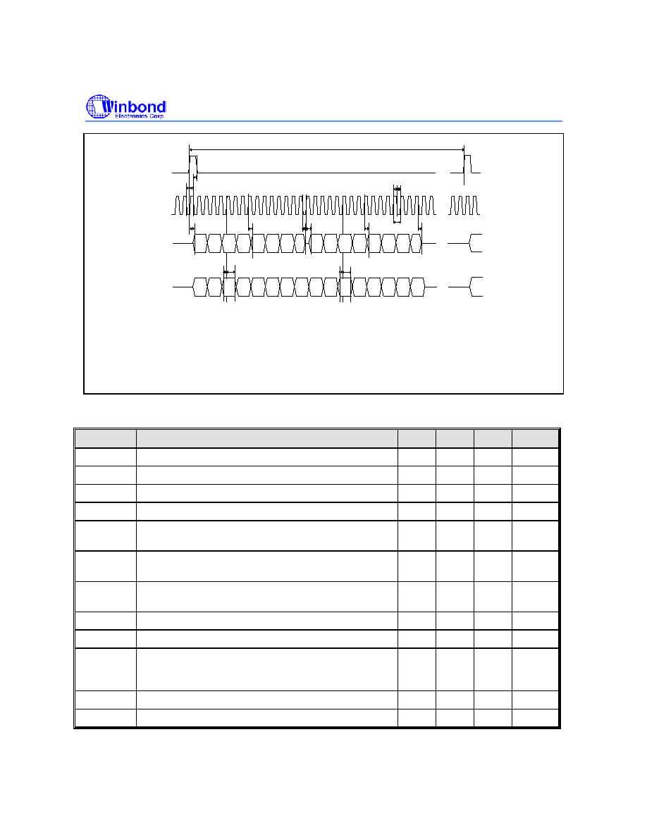
Figure 8.3 IDL PCM Timing
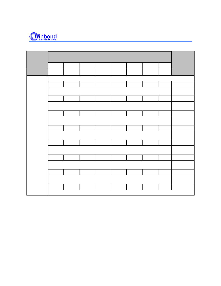
SYMBOL
DESCRIPTION
MIN
TYP
MAX
UNIT
1/T
FS
FST
Frequency
--- 8
--- kHz
1/T
BCK
BCLKT
Frequency
256 ---
4096
kHz
T
BCKH
BCLKT High Pulse Width
50
---
---
ns
T
BCKL
BCLKT Low Pulse Width
50
---
---
ns
T
FSRH
BCLKT ≠1 Falling Edge to FST Rising
Edge Hold Time
20 --- --- ns
T
FSRS
FST Rising Edge to BCLKT 0 Falling edge
Setup Time
60 --- --- ns
T
FSFH
BCLKT 0 Falling Edge to FST Falling Edge
Hold Time
20 --- --- ns
T
BDTD
BCLKT Rising Edge to Valid PCMT Delay
Time
10 --- 60 ns
T
HID
Delay Time from the BCLKT 8 Falling
Edge (B1 channel) or BCLKT 18 Falling
Edge (B2 Channel) to PCMT Output High
Impedance
10 --- 50 ns
T
DRS
Valid PCMR to BCLKT Falling Edge Setup
Time
20 --- --- ns
T
DRH
PCMR Hold Time from BCLKT Falling
Edge
75 --- --- ns
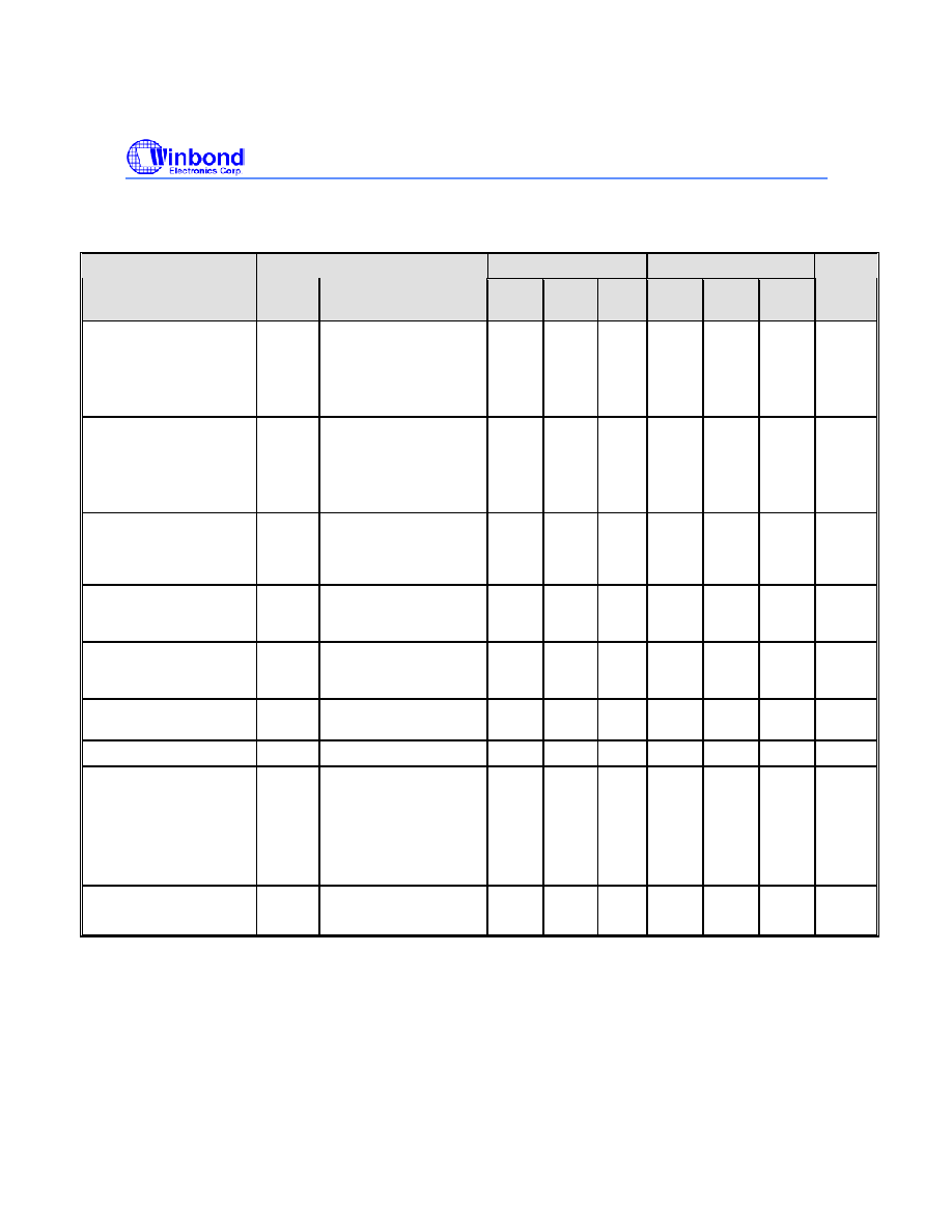
Table 8.3 IDL PCM Timing Parameters
F ST
B C L K T
PC M T
PC M R
D 7 D 6 D 5 D 4 D 3 D 2 D 1 D 0
D 7 D 6 D 5 D 4 D 3 D 2
D 1 D 0
D 7 D 6 D 5 D 4 D 3 D 2 D 1 D 0
D 7 D 6 D 5 D 4 D 3 D 2
D 1 D 0
0
1
2
3
4
5
6
7
8
9
10
11
12
13
14
15
16
17
18
T
F S
T
F SR H
T
F SF H
T
F SR S
T
B D T D
T
B D T D
T
B D T D
T
B D T D
T
H ID
T
H ID
T
D R S
T
D R S
T
D R H
T
D R H
B C H = 0
B 1 C hannel
B C H = 1
B 2 C hannel
M SB
M SB
M SB
M SB
L SB
L SB
L SB
L SB
T
B C K
T
B C K H
T
B C K L
-1
W6811
Publication Release Date: October 10, 2002
- 19 -
Revision A9
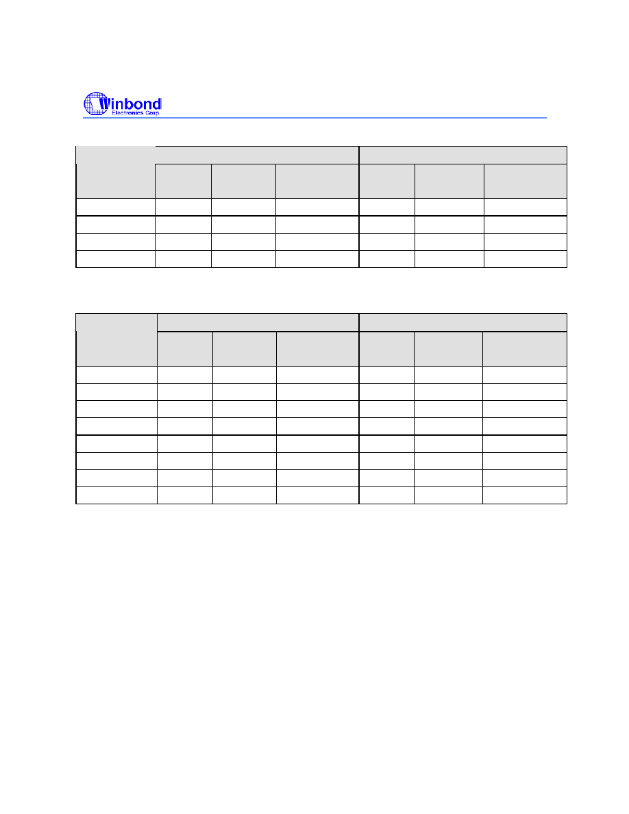
Figure 8.4 GCI PCM Timing
SYMBOL
DESCRIPTION
MIN
TYP
MAX UNIT
1/T
FST
FST
Frequency
--- 8 --- kHz
1/T
BCK
BCLKT
Frequency
512
--- 6176
kHz
T
BCKH
BCLKT High Pulse Width
50
---
---
ns
T
BCKL
BCLKT Low Pulse Width
50
---
---
ns
T
FSRH
BCLKT 0 Falling Edge to FST Rising Edge Hold
Time
20 --- --- ns
T
FSRS
FST Rising Edge to BCLKT 1 Falling edge Setup
Time
60 --- --- ns
T
FSFH
BCLKT 1 Falling Edge to FST Falling Edge Hold
Time
20 --- --- ns
T
FDTD
FST Rising Edge to Valid PCMT Delay Time
---
---
60
ns
T
BDTD
BCLKT Rising Edge to Valid PCMT Delay Time
---
---
60
ns
T
HID
Delay Time from the BCLKT 16 Falling Edge (B1
channel) or BCLKT 32 Falling Edge (B2 Channel) to
PCMT Output High Impedance
10 --- 50 ns
T
DRS
Valid PCMR to BCLKT Rising Edge Setup Time
20
---
---
ns
T
DRH
PCMR Hold Time from BCLKT Rising Edge
---
---
60
ns
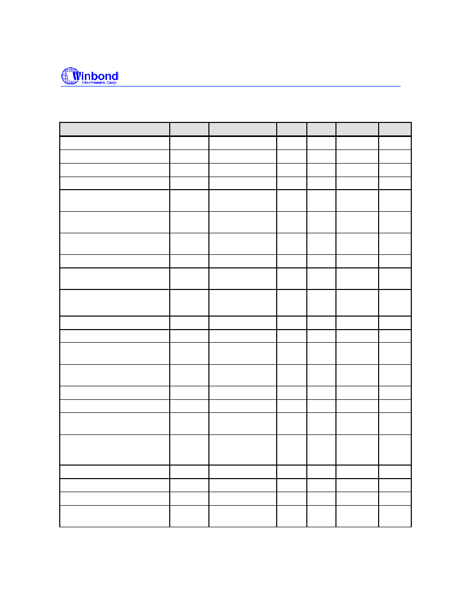
Table 8.4 GCI PCM Timing Parameters
FST
B C L K T
PC M T
PC M R
D 7 D 6 D 5 D 4 D 3 D 2 D 1 D 0
D 7 D 6 D 5 D 4 D 3 D 2
D 1 D 0
D 7 D 6 D 5 D 4 D 3 D 2 D 1 D 0 D 7 D 6 D 5 D 4 D 3 D 2 D1 D 0
T
FS
T
FD TD
T
B D TD
T
B D TD
T
B D T D
T
H ID
T
H ID
T
D R S
T
D R S
T
D R H
T
D R H
B C H = 0
B 1 C hannel
B C H = 1
B 2 C hannel
M SB
M SB
M SB
M SB
L SB
L SB
L SB
L SB
T
FSR H
T
FSFH
T
FSR S
T
B C K
T
B C K H
T
B C K L
2
3
4
5
6
7
8
9 10 11 12 13 14 15 16 17 18 19 20 21 22 23 24 25 26 27 28 29 30 31 32 33 34
1
0

W6811
- 20 -
SYMBOL
DESCRIPTION
MIN
TYP
MAX UNIT
1/T
MCK
Master Clock Frequency
---
256
512
1536
1544
2048
2560
4096
--- kHz
T
MCKH
/ T
MCK
MCLK Duty Cycle for 256 kHz
Operation
45%
55%
T
MCKH
Minimum Pulse Width High for MCLK(512 kHz or
Higher)
50 --- --- ns
T
MCKL
Minimum Pulse Width Low for MCLK (512 kHz or
Higher)
50 --- --- ns
T
FTRHM
MCLK falling Edge to FST Rising Edge Hold
Time
50 --- --- ns
T
FTRSM
FST Rising Edge to MCLK Falling edge Setup
Time
50 --- --- ns
T
RISE
Rise Time for All Digital Signals
---
---
50
ns
T
FALL
Fall Time for All Digital Signals
---
---
50
ns
Table 8.5 General PCM Timing Parameters
W6811
Publication Release Date: October 10, 2002
- 21 -
Revision A9
9. ABSOLUTE MAXIMUM RATINGS
9.1. A
BSOLUTE
M
AXIMUM
R
ATINGS
Condition
Value
Junction temperature
150
0
C
Storage temperature range
-65
0
C to +150
0
C
Voltage Applied to any pin Analog
Digital
(V
SSA
- 0.3V) to (V
DDA
+ 0.3V)
(V
SSD
- 0.3V) to (V
DDD
+ 0.3V)
Voltage applied to any pin Analog
(Input current limited to +/-20 mA) Digital
(V
SSA
≠ 1.0V) to (V
DDA
+ 1.0V)
(V
SSD
≠ 1.0V) to (V
DDD
+ 1.0V)
Lead temperature (soldering ≠ 10 seconds)
300
0
C
V
DDA
- V
SSA
; V
DDD
- V
SSD
-0.5V to +6V
V
DDD
≠ V
DDA
2
< 0.3V
1. Stresses above those listed may cause permanent damage to the device. Exposure to the absolute
maximum ratings may affect device reliability. Functional operation is not implied at these conditions.
2. At any time, the digital power supply should not be higher the 0.3V from the analog power supply.
9.2. O
PERATING
C
ONDITIONS
Condition
Value
Industrial operating temperature
-40
0
C to +85
0
C
Analog supply voltage (V
DDA
)
+4.5V to +5.5V
Digital supply voltage (V
DDD
)
+2.7V to +3.3V
Ground voltage (V
SSA,
V
SSD
) 0V
Note: Exposure to conditions beyond those listed under Absolute Maximum Ratings may adversely
affect the life and reliability of the device.
W6811
- 22 -
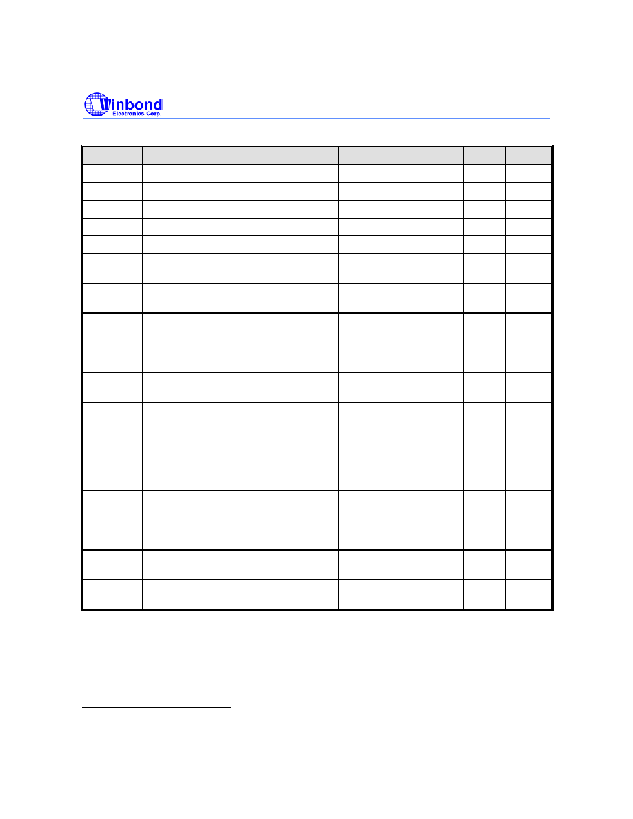
10. ELECTRICAL CHARACTERISTICS
10.1. G
ENERAL
P
ARAMETERS
Symbol Parameters
Conditions
Min
(2)
Typ
(1)
Max
(2)
Units
V
IL
Input Low Voltage
0.5
V
V
IH
Input High Voltage
2.2
V
V
OL
PCMT Output Low Voltage
I
OL
= 1.6 mA
0.4
V
V
OH
PCMT Output High Voltage
I
OL
= -1.6 mA
V
DDD
≠ 0.5
V
I
DDA
I
DDD
V
DDA
Current (Operating) -ADC+DAC
PUI = 1
FSX running MCLK
running
5.5
25
8
1000
mA
µA
I
SBA
I
SBD
V
CCA
Current (Standby)
PUI = 1
FSX = 0 MCLK running
200
0.2
500
100
nA
µA
I
PDA
I
PDD
V
CCA
Current (Power Down)
V
CCD
Current (Power Down)
PUI = 0
PUI = 0
200
200
500
500
nA
nA
I
IL
Input Leakage Current
V
SSD
<V
IN
<V
DDD
+/-10
µA
I
OL
PCMT Output Leakage Current
V
SSA
<PCMT<V
DDA
High Z State
+/-10
µA
C
IN
Digital Input Capacitance
10
pF
C
OUT
PCMT Output Capacitance
PCMT High Z
15
pF
1. Typical values: T
A
= 25∞C ,
V
DDA
= 5.0 V,
V
DDD
= 3.0 V
2. All min/max limits are guaranteed by Winbond via electrical testing or characterization. Not all
specifications are 100 percent tested.
W6811
Publication Release Date: October 10, 2002
- 23 -
Revision A9
10.2. A
NALOG
S
IGNAL
L
EVEL AND
G
AIN
P
ARAMETERS
V
DDA
=5V
±10%; V
SSA
=0V; T
A
=-40
∞C to +85∞C; all analog signals referred to V
AG
;
TRANSMIT
(A/D)
RECEIVE
(D/A)
UNIT
PARAMETER SYM.
CONDITION
TYP.
MIN.
MAX.
MIN. MAX.
Absolute
Level
L
ABS
0 dBm0 = 0dBm @ 600
1.096
--- --- --- --- V
PK
Max. Transmit
Level
T
XMAX
3.17 dBm0 for
µ-Law
3.14 dBm0 for A-Law
1.579
1.573
---
---
---
---
---
---
---
---
V
PK
V
PK
Absolute Gain
(0 dBm0 @
1020 Hz;
T
A
=+25
∞C)
G
ABS
0 dBm0 @ 1020 Hz;
T
A
=+25
∞C
0 -0.25
+0.25
-0.25
+0.2
5
dB
Absolute Gain
variation with
Temperature
G
ABS
T
T
A
=0
∞C to T
A
=+70
∞C
T
A
=-40
∞C to T
A
=+85
∞C
0 -0.03
-0.05
+0.03
+0.05
-0.03
-0.05
+0.0
3
+0.0
5
dB
Frequency
Response,
Relative to
0dBm0 @
1020 Hz
G
RTV
15
Hz
50 Hz
60 Hz
200 Hz
300 to 3000 Hz
3300 Hz
3400 Hz
3600 Hz
4000 Hz
4600 Hz to 100 kHz
---
---
---
---
---
---
---
---
---
---
---
---
---
-1.0
-0.20
-0.35
-0.8
---
---
---
-40
-30
-26
-0.4
+0.15
+0.15
0
0
-14
-32
-0.5
-0.5
-0.5
-0.5
-0.20
-0.35
-0.8
---
---
---
0
0
0
0
+0.1
5
+0.1
5
0
0
-14
-30
dB
Gain Variation
vs. Level Tone
(1020 Hz
relative to ≠10
dBm0)
G
LT
+3 to ≠40 dBm0
-40 to ≠50 dBm0
-50 to ≠55 dBm0
---
---
---
-0.3
-0.6
-1.6
+0.3
+0.6
+1.6
-0.2
-0.4
-1.6
+0.2
+0.4
+1.6
dB
W6811
- 24 -
10.3. A
NALOG
D
ISTORTION AND
N
OISE
P
ARAMETERS
V
DDA
=5V
±10%; V
SSA
=0V; T
A
=-40
∞C to +85∞C; all analog signals referred to V
AG
;
TRANSMIT (A/D)
RECEIVE (D/A)
PARAMETER
SYM.
CONDITION
MIN.
TYP.
MAX
.
MIN.
TYP.
MAX.
UNIT
Total Distortion vs. Level
Tone (1020 Hz,
µ-Law,
C-Message Weighted)
D
LT
µ
+3 dBm0
0 dBm0 to -30 dBm0
-40 dBm0
-45 dBm0
36
36
29
25
---
---
---
---
---
---
---
---
34
36
30
25
---
---
---
---
---
---
---
---
dBC
Total Distortion vs. Level
Tone (1020 Hz, A-Law,
Psophometric Weighted)
D
LTA
+3
dBm0
0 dBm0 to -30 dBm0
-40 dBm0
-45 dBm0
36
36
29
25
---
---
---
---
---
---
---
---
34
36
30
25
---
---
---
---
---
---
---
---
dBp
Spurious Out-Of-Band at
RO- (300 Hz to 3400 Hz
@ 0dBm0)
D
SPO
4600 Hz to 7600 Hz
7600 Hz to 8400 Hz
8400 Hz to 100000 Hz
---
---
---
---
---
---
---
---
---
---
---
---
---
---
---
-30
-40
-30
dB
Spurious In-Band (700
Hz to 1100 Hz @
0dBm0)
D
SPI
300 to 3000 Hz
---
--- -47
---
--- -47
dB
Intermodulation
Distortion (300 Hz to
3400 Hz ≠4 to ≠21 dBm0
D
IM
Two
tones
--- --- -41
--- --- -41 dB
Crosstalk (1020 Hz @
0dBm0)
D
XT
--- --- -75
--- --- -75 dBm0
Absolute Group Delay
ABS
1200
Hz
--- --- 360
--- --- 240
µsec
Group Delay Distortion
(relative to group delay
@ 1200 Hz)
D
500 Hz
600 Hz
1000 Hz
2600 Hz
2800 Hz
---
---
---
---
---
---
---
---
---
---
750
380
130
130
750
---
---
---
---
---
---
---
---
---
---
750
370
120
120
750
µsec
Idle Channel Noise
N
IDL
µ-Law; C-message
A-Law; Psophometric
---
---
---
---
5
-69
---
---
---
---
13
-79
dBrnc
dBm0p
W6811
Publication Release Date: October 10, 2002
- 25 -
Revision A9
10.4. A
NALOG
I
NPUT AND
O
UTPUT
A
MPLIFIER
P
ARAMETERS
V
DDA
=5V
±10%; V
SSA
=0V; T
A
=-40
∞C to +85∞C; all analog signals referred to V
AG
;
PARAMETER
SYM.
CONDITION
MIN.
TYP.
MAX.
UNIT.
AI Input Offset Voltage
V
OFF,AI
AI+,
AI-
--- ---
±25
mV
AI Input Current
I
IN,AI
AI+,
AI-
---
±0.1
±1.0
µA
AI Input Resistance
R
IN,AI
AI+, AI- to V
AG
10 --- ---
M
AI Input Capacitance
C
IN,AI
AI+,
AI-
--- --- 10
pF
AI Common Mode Input
Voltage Range
V
CM,AI
AI+,
AI-
1.2 --- V
DDA
-1.2 V
AI Common Mode Rejection
Ratio
CMRR
TI
AI+,
AI-
---
60
---
dB
AI Amp Gain Bandwidth
Product
GBW
TI
AO, R
LD
10k
--- 2150
---
kHz
AI Amp DC Open Loop Gain
G
TI
AO, R
LD
10k
--- 95 ---
dB
AI Amp Equivalent Input
Noise
N
TI
C-Message
Weighted
--- -24
---
dBrnC
AO Output Voltage Range
V
TG
R
LD
=10k
to V
AG
R
LD
=2k
to V
AG
0.5
1.0
---
---
V
DDA
-0.5
V
DDA
-1.0
V
Load Resistance
R
LDTGRO
AO, RO to V
AG
2 --- ---
k
Load Capacitance
C
LDTGRO
AO,
RO
---
--- 100
pF
AO & RO Output Current
I
OUT1
0.5
AO,RO-
V
DDA
-0.5
±1.0
--- ---
mA
RO- Output Resistance
R
RO-
RO-, 0 to 3400
Hz
--- 1 ---
RO- Output Offset Voltage
V
OFF,RO-
RO- to V
AG
---
---
±25
mV
Analog Ground Voltage
V
AG
Relative to V
SSA
2.429 2.5 2.573
V
V
AG
Output Resistance
R
VAG
Within
±25mV
change
--- 2.5 12.5
Power Supply Rejection Ratio
(0 to 100 kHz to V
DDA
, C-
message)
PSRR Transmit
Receive
30
30
80
75
---
---
dBC
PAI Input Offset Voltage
V
OFF,PAI
PAI
--- ---
±20
mV
PAI Input Current
I
IN,PAI
PAI
---
±0.05 ±1.0
µA
PAI Input Resistance
R
IN,PAI
PAI to V
AG
10
---
---
M
PAI Amp Gain Bandwidth
Product
GBW
PI
PAO- no load
---
1000
---
kHz
W6811
- 26 -
PARAMETER
SYM.
CONDITION
MIN.
TYP.
MAX.
UNIT.
Output Offset Voltage
V
OFF,PO
PAO+ to PAO-
---
---
±50
mV
Load Resistance
R
LDPO
PAO+,
PAO-
differentially
300 --- ---
Load Capacitance
C
LDPO
PAO+,
PAO-
differentially
--- --- 1000 pF
PO Output Current
I
OUTPO
0.5
AO,RO-
V
DDA
-0.5
±10.0 --- ---
mA
PO Output Resistance
R
PO
PAO+ to PAO-
---
1
---
PO Differential Gain
G
PO
R
LD
=300
,
+3dBm0, 1 kHz,
PAO+ to PAO-
-0.2 0 +0.2
dB
PO Differential Signal to
Distortion C-Message
weighted
D
PO
Z
LD
=300
Z
LD
=100nF +
100
Z
LD
=100nF + 20
45
---
---
60
40
40
---
---
---
dBC
PO Power Supply Rejection
Ratio (0 to 25 kHz to V
DDA
,
Differential out)
PSRR
PO
0 to 4 kHz
4 to 25 kHz
40
---
55
40
---
---
dB
W6811
Publication Release Date: October 10, 2002
- 27 -
Revision A9
10.5. D
IGITAL
I/O
10.5.1.
µ-Law Encode Decode Chatacteristics
Digital Code
D7 D6 D5 D4 D3 D2 D1 D0
Normalized
Encode
Decision
Levels
Sign Chord Chord Chord Step Step Step Step
Normalized
Decode
Levels
1 0 0 0 0 0 0 0 8031
:
1 0 0 0 1 1 1 1 4191
:
1 0 0 1 1 1 1 1 2079
:
1 0 1 0 1 1 1 1 1023
:
1 0 1 1 1 1 1 1 495
:
1 1 0 0 1 1 1 1 231
:
1 1 0 1 1 1 1 1 99
:
1 1 1 0 1 1 1 1 33
:
1 1 1 1 1 1 1 0 2
1 1 1 1 1 1 1 1 0
8159
7903
:
4319
4063
:
2143
2015
:
1055
991
:
511
479
:
239
223
:
103
95
:
35
31
:
3
1
0
Notes:
Sign bit = 0 for negative values, sign bit = 1 for positive values
W6811
- 28 -
10.5.2. A-Law Encode Decode Characteristics
Digital Code
D7 D6 D5 D4 D3 D2 D1 D0
Normalized
Encode
Decision
Levels
Sign Chord Chord Chord Step Step Step Step
Normalized
Decode
Levels
1 0 1 0 1 0 1 0 4032
:
1 0 1 0 0 1 0 1 2112
:
1 0 1 1 0 1 0 1 1056
:
1 0 0 0 0 1 0 1 528
:
1 0 0 1 0 1 0 1 264
:
1 1 1 0 0 1 0 1 132
:
1 1 1 0 0 1 0 1 66
:
1 1 0 1 0 1 0 1 1
4096
3968
:
2048
2048
:
1088
1024
:
544
512
:
272
256
:
136
128
:
68
64
:
2
0
Notes:
1. Sign bit = 0 for negative values, sign bit = 1 for positive values
2. Digital code includes inversion of all even number bits
W6811
Publication Release Date: October 10, 2002
- 29 -
Revision A9
10.5.3. PCM Codes for Zero and Full Scale
µ-Law
A-Law
Level
Sign bit
(D7)
Chord bits
(D6,D5,D4)
Step bits
(D3,D2,D1,D0)
Sign bit
(D7)
Chord bits
(D6,D5,D4)
Step bits
(D3,D2,D1,D0)
+ Full Scale
1
000
0000
1
010
1010
+ Zero
1
111
1111
1
101
0101
- Zero
0
111
1111
0
101
0101
- Full Scale
0
000
0000
0
010
1010
10.5.4. PCM Codes for 0dBm0 Output
µ-Law
A-Law
Sample
Sign bit
(D7)
Chord bits
(D6,D5,D4)
Step bits
(D3,D2,D1,D0)
Sign bit
(D7)
Chord bits
(D6,D5,D4)
Step bits
(D3,D2,D1,D0)
1 0
001
1110
0
011
0100
2 0
000
1011
0
010
0001
3 0
000
1011
0
010
0001
4 0
001
1110
0
011
0100
5 1
001
1110
1
011
0100
6 1
000
1011
1
010
0001
7 1
000
1011
1
010
0001
8 1
001
1110
1
011
0100
W6811
- 30 -
11. TYPICAL APPLICATION CIRCUIT
0.1
µ
F
27k
27k
-
V
AUDIOOUT
+
V
DDA
Power
Control
2.048 MHz
PCM OUT
PCM IN
8 kHz
V
DDD
27k
0.01
µ
F
27k
27k
27k
1.0
µ
F
1.0
µ
F
V
AUDIOIN
-
V
AUDIOIN+
V
AG
24
AI+ 23
AI- 22
AO 21
µ
/A 20
V
SSA
19
FSX 16
PCMO 15
BCLKT 14
MCLK 13
1 V
REF
2 RO -
3 PAI
4 PAO -
5 PAO+
6 V
DDA
9 FSR
10 PCMI
11 BCLKR
12 PUI
PDIP/SOG/SSOP/TSSOP
V
SSD
17
8 V
DDD
NC 18
7 NC
V
DDD
0.1
µ
F
0.1
µ
F
-
+
V
DDA
Power
Control
2.048 MHz
PCM OUT
PCM IN
8 kHz
V
DDD
0.01
µ
F
27k
1.0
µ
F
µ
V
AUDIOIN
-
V
AUDIOIN+
V
AG
24
AI+ 23
AI- 22
AO 21
µ
/A 20
V
SSA
19
FSX 16
PCMO 15
BCLKT 14
MCLK 13
1 V
REF
2 RO -
3 PAI
4 PAO -
5 PAO+
6 V
DDA
9 FSR
10 PCMI
11 BCLKR
12 PUI
V
SSD
17
8 V
DDD
NC 18
7 NC
V
AG
24
AI+ 23
AI- 22
AO 21
µ
/A 20
V
SSA
19
FST 16
PCMT 15
BCLKT 14
MCLK 13
1 V
REF
2 RO -
3 PAI
4 PAO -
5 PAO+
6 V
DDA
9 FSR
10 PCMR
11 BCLKR
12 PUI
V
SSD
17
8 V
DDD
NC 18
7 NC
V
DDD
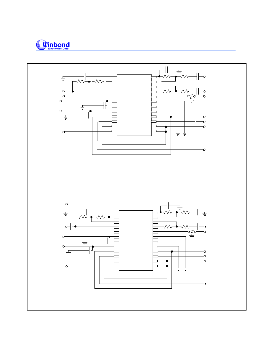
Figure 11.1 Typical circuit for Differential Analog I/O's
0.1
µ
F
27k
27k
2.048 MHz
PCM OUT
PCM IN
8 kHz
V
DD
27k
0.01
µF
27k
27k
27k
1.0
µ
F
1.0
µ
F
V
AUDIOIN
AUDIO OUT
R
L
2k
100
µ
F
AUDIO OUT
R
L
150
Power
Control
V
AG
24
AI+ 23
AI- 22
AO 21
µ/A 20
V
SSA
19
FSX 16
PCMO 15
BCLKT 14
MCLK 13
1 V
REF
2 RO-
3 PAI
4 PAO-
5 PAO+
6 V
DDA
9 FSR
10 PCMI
11 BCLKR
12 PUI
PDIP/SOG/SSOP/TSSOP
V
SSD
17
8 V
DDD
NC 18
7 NC
V
DDA
V
DDD
0.1
µ
F
0.1
µ
F
27k
27k
2.048 MHz
PCM OUT
PCM IN
8 kHz
V
DD
27k
1.0
µ
F
V
AUDIOIN
AUDIO OUT
R
L
2k
100
µ
F
AUDIO OUT
R
L
150
Power
Control
V
AG
24
AI+ 23
AI- 22
AO 21
µ/A 20
V
SSA
19
FSX 16
PCMO 15
BCLKT 14
MCLK 13
1 V
REF
2 RO-
3 PAI
4 PAO-
5 PAO+
6 V
DDA
9 FSR
10 PCMI
11 BCLKR
12 PUI
V
SSD
17
8 V
DDD
NC 18
7 NC
V
AG
24
AI+ 23
AI- 22
AO 21
µ/A 20
V
SSA
19
FST 16
PCMT 15
BCLKT 14
MCLK 13
1 V
REF
2 RO-
3 PAI
4 PAO-
5 PAO+
6 V
DDA
9 FSR
10 PCMR
11 BCLKR
12 PUI
V
SSD
17
8 V
DDD
NC 18
7 NC
V
DDA
V
DDD
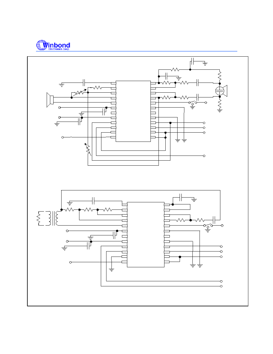
Figure 11.2 Typical circuit for Single Ended Analog I/O's
W6811
Publication Release Date: October 10, 2002
- 31 -
Revision A9
0.1
µ
F
27k
2.048 MHz
PCM OUT
PCM IN
8 kHz
V
DD
1k
0.01
µ
F
100k
100k
1k
1.0
µ
F
1.0
µ
F
27k
1.5k
1.5k
Electret
Microphone
WM
-
54B Panasonic
27k
Speake
Power
Control
1k
200
p
F
V
AG
24
AI+ 23
AI- 22
AO 21
µ
/A 20
V
SSA
19
FSX 16
PCMO 15
BCLKT 14
MCLK 13
1 V
REF
2 RO -
3 PAI
4 PAO -
5 PAO+
6 V
DDA
9 FSR
10 PCMI
11 BCLKR
12 PUI
PDIP/SOG/SSOP/TSSOP
V
SSD
17
8 V
DDD
NC 18
7 NC
V
DDA
V
DDD
0.1
µ
F
0.1
µ
F
27k
2.048 MHz
PCM OUT
PCM IN
8 kHz
V
DD
0.01
µ
F
1k
1.0
µ
F
27k
27k
1.5k
1.5k
Electret
Microphone
WM
-
54B Panasonic
Speake
Power
Control
1k
200
p
F
V
AG
24
AI+ 23
AI- 22
AO 21
µ
/A 20
V
SSA
19
FSX 16
PCMO 15
BCLKT 14
MCLK 13
1 V
REF
2 RO -
3 PAI
4 PAO -
5 PAO+
6 V
DDA
9 FSR
10 PCMI
11 BCLKR
12 PUI
V
SSD
17
8 V
DDD
NC 18
7 NC
V
AG
24
AI+ 23
AI- 22
AO 21
µ
/A 20
V
SSA
19
FST 16
PCMT 15
BCLKT 14
MCLK 13
1 V
REF
2 RO -
3 PAI
4 PAO -
5 PAO+
6 V
DDA
9 FSR
10 PCMR
11 BCLKR
12 PUI
V
SSD
17
8 V
DDD
NC 18
7 NC
V
DDA
V
DDD
Figure 11.3 Handset Interface
0.1
µ
F
27k
27k
4.096 MHz
PCM OUT
PCM IN
8 kHz
V
DD
27k
0.01
µF
27k
1.0
µ
F
600
N=
1
N=
1
TIP
RI
NG
600
B1 ≠ 0V
B2 - +5V
Power
Control
V
AG
24
AI+ 23
AI- 22
AO 21
µ/A 20
V
SSA
19
FSX 16
PCMO 15
BCLKT 14
MCLK 13
1 V
REF
2 RO-
3 PAI
4 PAO-
5 PAO+
6 V
DDA
9 FSR
10 PCMI
11 BCLKR
12 PUI
PDIP/SOG/SSOP/TSSOP
V
SSD
17
8 V
DDD
NC 18
7 NC
V
DDD
0.1
µ
F
0.1
µ
F
27k
4.096 MHz
PCM OUT
PCM IN
8 kHz
V
DD
600
N=
1
N=
1
600
N=
1
N=
1
TIP
RI
NG
600
B1 ≠ 0V
B2 - +5V
Power
Control
V
AG
24
AI+ 23
AI- 22
AO 21
µ/A 20
V
SSA
19
FSX 16
PCMO 15
BCLKT 14
MCLK 13
1 V
REF
2 RO-
3 PAI
4 PAO-
5 PAO+
6 V
DDA
9 FSR
10 PCMI
11 BCLKR
12 PUI
PDIP/SOG/SSOP/TSSOP
V
SSD
17
8 V
DDD
NC 18
7 NC
V
AG
24
AI+ 23
AI- 22
AO 21
µ/A 20
V
SSA
19
FST 16
PCMT 15
BCLKT 14
MCLK 13
1 V
REF
2 RO-
3 PAI
4 PAO-
5 PAO+
6 V
DDA
9 FSR
10 PCMR
11 BCLKR
12 PUI
PDIP/SOG/SSOP/TSSOP
V
SSD
17
8 V
DDD
NC 18
7 NC
V
DDD
Figure 11.4 Transformer Interface Circuit in GCI mode
W6811
- 32 -
12. PACKAGE SPECIFICATION
12.1. 24L TSSOP - 4.4X7.8
MM
PLASTIC THIN SHRINK SMALL OUTLINE PACKAGE (TSSOP) DIMENSIONS
DIMENSION IN MM
DIMENSION IN INCH
SYMBOL
MIN NOM MAX MIN NOM MAX
A
1.20
0.043
A1 0.05 0.15
0.002 0.006
A2 0.80 0.90 1.05 0.031 0.035 0.041
L 0.50 0.60 0.75 0.020 0.024 0.030
E
6.40 BSC.
0.252 BSC.
HE 4.30 4.40 4.50 0.169 0.173 0.177
D 7.70 7.80 7.90 0.303 0.307 0.311
b 0.19 0.30
0.007 0.012
c 0.09 0.20
0.004 0.008
L1
1.0 REF.
0.039 REF
e
0.65 BSC.
0.026 BSC
01 0 8 0 8
W6811
Publication Release Date: October 10, 2002
- 33 -
Revision A9
12.2. 24L SOP-300
MIL
SMALL OUTLINE PACKAGE (SAME AS SOG & SOIC) DIMENSIONS
DIMENSIONS IN MM
DIMENSIONS IN INCH
SYMBOL
MIN MAX MIN MAX
A 2.35
2.65
0.093
0.104
A1 0.10
0.30
0.004
0.012
b 0.33
0.51
0.013
0.020
c 0.23
0.32
0.009
0.013
E 7.40
7.60
0.291
0.299
D 12.60
13.00
0.946
0.512
e
1.27 BSC.
0.050 BSC.
H
E
10.00 1065 0.394 0.419
Y
0.10
0.004
L 0.40
1.27
0.016
0.050
0 0
8
0
8
E
1
20
11
10
GAUGE PLANE
SEATING PLANE

W6811
- 34 -
12.3. 24L SSOP-150
MIL
SHRINK SMALL OUTLINE PACKAGE DIMENSIONS
DIMENSION IN MM
DIMENSION IN INCH
SYMBOL
MIN NOM MAX MIN NOM MAX
A
1.63
1.78
0.064
0.070
A1 0.10
0.004
A2
1.50
0.059
b 0.20 0.30
0.008 0.012
c 0.18 0.25
0.006 0.010
D 8.50 8.65 8.80 0.335 0.341 0.346
H
E
5.80 6.00 6.20 0.228 0.236 0.244
E 3.81 3.91 4.00 0.150 0.154 0.157
e 0.50
0.635
0.76
0.020 0.025 0.030
L 0.40
0.64 0.016
0.025
L1 1.04
0.041
Y
0.10
0.004
0 0 8 0 8
H
W6811
Publication Release Date: October 10, 2002
- 35 -
Revision A9
12.4. 24L PDIP
≠ 300
MIL
PLASTIC DUAL INLINE PACKAGE DIMENSIONS
DIMENSION IN MM
DIMENSION IN INCH
SYMBOL
MIN NOM MAX MIN NOM MAX
A
4.45
0.175
A1 0.25
0.010
A2 3.18 3.30 3.43 0.125 0.130 0.135
B 0.41 0.46 0.56 0.016 0.018 0.022
B1 1.47 1.52 1.63 0.058 0.060 0.064
c 0.20 0.25 0.36 0.008 0.010 0.014
D 31.95
32.26 1.258
1.270
E 7.37 7.62 7.87 0.290 0.300 0.310
E1 6.43 6.55 6.68 0.253 0.258 0.263
e1 2.29 2.54 2.79 0.090 0.100 0.110
L 3.05 3.30 3.56 0.120 0.130 0.140
· 0∞ 15∞ 0∞ 15∞
e
A
8.38 8.89 9.40 0.330 0.350 0.370
S
2.29
0.090
e
A
2
A
c
E
Base Plane
Mounting Plane
1
A
1
e
L
A
S
1
E
D
1
B
B
24
1
12
13
·

W6811
- 36 -
13. ORDERING INFORMATION
Part
Number
Description
When ordering W6811 series devices, please refer to the following part numbers.
Part Number
W6811IW
W6811IS
W6811IR
W6811IE
Package Type:
W
=
24-Lead Plastic Thin Small Outline Package (TSSOP) Type 1
S
=
24-Lead Plastic Small Outline Package (SOG/SOP)
R
=
24-Lead Plastic Small Outline Package (SSOP)
E
=
24-Lead Plastic Dual Inline Package (PDIP)
Product Family
W6811 Product
W6811I _
W6811
Publication Release Date: October 10, 2002
- 37 -
Revision A9
14. VERSION HISTORY
VERSION DATE PAGE
DESCRIPTION
A7 August
9,
2002
Preliminary
A8 Septembe
r 26, 2002
A9 October
10, 2002
Headquarters
Winbond Electronics Corporation America
Winbond Electronics (Shanghai) Ltd.
No. 4, Creation Rd. III
2727 North First Street, San Jose,
27F, 299 Yan An W. Rd. Shanghai,
Science-Based Industrial Park, CA 95134, U.S.A.
200336 China
Hsinchu, Taiwan
TEL: 1-408-9436666
TEL: 86-21-62365999
TEL: 886-3-5770066
FAX: 1-408-5441798
FAX: 86-21-62356998
FAX: 886-3-5665577
http://www.winbond-usa.com/
http://www.winbond.com.tw/
Taipei Office
Winbond Electronics Corporation Japan Winbond Electronics (H.K.) Ltd.
9F, No. 480, Pueiguang Rd. 7F Daini-ueno BLDG, 3-7-18
Unit 9-15, 22F, Millennium City,
Neihu District,
Shinyokohama Kohoku-ku,
No. 378 Kwun Tong Rd.,
Taipei, 114, Taiwan
Yokohama, 222-0033
Kowloon, Hong Kong
TEL: 886-2-81777168
TEL: 81-45-4781881
TEL: 852-27513100
FAX: 886-2-87153579
FAX: 81-45-4781800
FAX: 852-27552064
Please note that all data and specifications are subject to change without notice.
All the trademarks of products and companies mentioned in this datasheet belong to their respective owners.
The information contained in this datasheet may be subject to change without
notice. It is the responsibility of the customer to check the Winbond USA website
(
www.winbond-usa.com
) periodically for the latest version of this document, and
any Errata Sheets that may be generated between datasheet revisions.