W6811
- 2 -
1. GENERAL DESCRIPTION
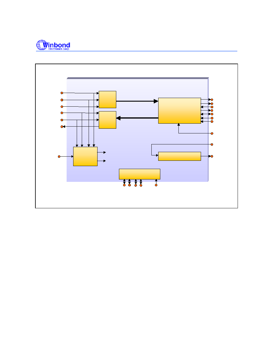
The W6811 is a general-purpose single channel PCM CODEC with pin-selectable
µ-Law or A-Law
companding. The device is compliant with the ITU G.712 specification. It operates off of a separated
analog (5V) and digital (3V) power supplies and is available in 24-pin PDIP, SOG, SSOP, and TSSOP
package options. Functions performed include digitization and reconstruction of voice signals, and
band limiting and smoothing filters required for PCM systems. The filters are compliant with ITU G.712
specification. W6811 performance is specified over the industrial temperature range of ≠40
∞C to
+85
∞C.
The W6811 includes an on-chip precision voltage reference and an additional power amplifier,
capable of driving 300
loads differentially up to a level of 6.3V peak-to-peak. The analog section is
fully differential, reducing noise and improving the power supply rejection ratio. The data transfer
protocol supports both long-frame and short-frame synchronous communications for PCM
applications, and IDL and GCI communications for ISDN applications. W6811 accepts seven master
clock rates between 256 kHz and 4.096 MHz, and an on-chip pre-scaler automatically determines the
division ratio for the required internal clock.
2. FEATURES
∑ Power supply:
Analog 4.5 ≠ 5.5V
Digital 2.7 ≠ 3.3V
∑ Typical power dissipation of 25 mW,
power-down mode of 0.5
µW
∑ Fully-differential analog circuit design
∑ On-chip precision reference of 1.575 V for
a 0 dBm TLP at 600
∑ Push-pull power amplifiers with external
gain adjustment with 300
load capability
∑ Seven master clock rates of 256 kHz to
4.096 MHz
∑ Pin-selectable
µ-Law and A-Law
companding (compliant with ITU G.711)
∑ CODEC A/D and D/A filtering compliant
with ITU G.712
∑ Industrial temperature range (≠40∞C to
+85
∞C)
∑ Four packages: 24-pin PDIP, SOG, SSOP,
and TSSOP
APPLICATIONS
∑ Digital Telephone Systems
∑ Central Office Equipment (Gateways,
Switches, Routers)
∑ PBX Systems (Gateways, Switches)
∑ PABX/SOHO Systems
∑ Local Loop card
∑ SOHO Routers
∑ VoIP Terminals
∑ Enterprise Phones
∑ ISDN Terminals
∑ Analog line cards
∑ Digital Voice Recorders

W6811
- 4 -
4. TABLE OF CONTENTS
1. GENERAL DESCRIPTION ................................................................................................................. 2
2. FEATURES ......................................................................................................................................... 2
3. BLOCK DIAGRAM .............................................................................................................................. 3
4. TABLE OF CONTENTS ...................................................................................................................... 4
5. PIN CONFIGURATION ....................................................................................................................... 6
6. PIN DESCRIPTION............................................................................................................................. 7
7. FUNCTIONAL DESCRIPTION............................................................................................................ 9
7.1. Transmit Path............................................................................................................................. 9
7.2. Receive Path............................................................................................................................ 10
7.3. Power Management................................................................................................................. 11
7.3.1. Analog Supply ................................................................................................................ 11
7.3.2. Digital Supply ................................................................................................................. 11
7.3.3. Analog Ground Reference Bypass................................................................................. 11
7.3.4. Analog Ground Reference Voltage Output .................................................................... 11
7.4. PCM Interface .......................................................................................................................... 11
7.4.1. Long Frame Sync ........................................................................................................... 12
7.4.2. Short Frame Sync .......................................................................................................... 12
7.4.3. GCI Interface .................................................................................................................. 12
7.4.4. IDL Interface................................................................................................................... 13
7.4.5. System Timing................................................................................................................ 13
8. TIMING DIAGRAMS.......................................................................................................................... 14
9. ABSOLUTE MAXIMUM RATINGS.................................................................................................... 21
9.1. Absolute Maximum Ratings ................................................................................................... 21
9.2. Operating Conditions ............................................................................................................. 21
10. ELECTRICAL CHARACTERISTICS ............................................................................................... 22
10.1. General Parameters .............................................................................................................. 22
10.2. Analog Signal Level and Gain Parameters............................................................................ 23
10.3. Analog Distortion and Noise Parameters .............................................................................. 24
10.4. Analog Input and Output Amplifier Parameters ..................................................................... 25
10.5. Digital I/O ............................................................................................................................... 27
10.5.1. µ-Law Encode Decode Characteristics........................................................................ 27
10.5.2. A-Law Encode Decode Characteristics ....................................................................... 28
10.5.3. PCM Codes for Zero and Full Scale ............................................................................ 29
10.5.4. PCM Codes for 0dBm0 Output .................................................................................... 29
11. TYPICAL APPLICATION CIRCUIT................................................................................................. 30

W6811
Publication Release Date: October 23, 2003
- 5 -
Revision A10
12. PACKAGE SPECIFICATION .......................................................................................................... 32
12.1. 24L TSSOP ≠ 4.4X7.8mm ..................................................................................................... 32
12.2. 24L SOP ≠ 300mil.................................................................................................................. 33
12.3. 24L SSOP ≠ 209mil ............................................................................................................... 34
12.4. 24L PDIP ≠ 300 mil ................................................................................................................ 35
13. ORDERING INFORMATION........................................................................................................... 36
14. VERSION HISTORY ....................................................................................................................... 37