Document Outline
- Main Menu
- 4-bit µC Products
- Search
- Web

W741E260
4-BIT FLASH MICROCONTROLLER
Publication Release Date: March 1998
- 1 -
Revision A2
Table of Contents--
GENERAL DESCRIPTION .............................................................................................................................. 2
FEATURES...................................................................................................................................................... 2
PIN CONFIGURATION.................................................................................................................................... 4
PIN DESCRIPTION ......................................................................................................................................... 5
BLOCK DIAGRAM........................................................................................................................................... 6
FUNCTIONAL DESCRIPTION ........................................................................................................................ 7
ABSOLUTE MAXIMUM RATINGS ................................................................................................................ 37
DC CHARACTERISTICS............................................................................................................................... 37
AC CHARACTERISTICS............................................................................................................................... 39
PAD ASSIGNMENT AND POSITIONS.......................................................................................................... 39
TYPICAL APPLICATION CIRCUIT................................................................................................................ 41
INSTRUCTION SET TABLE.......................................................................................................................... 42
PACKAGE DIMENSIONS.............................................................................................................................. 93

W741E260
- 2 -
GENERAL DESCRIPTION
The W741E260 is a high-performance 4-bit microcontroller (
µC) that provides an LCD driver and the
flash EEPROM for the program memory. The device contains a 4-bit ALU, two 8-bit timers, two
dividers (for two oscillators) in dual-clock operation, a 32
◊ 4 LCD driver, and five 4-bit I/O ports
(including 1 output port for LED driving). There are also five interrupt sources and 8-level subroutine
nesting for interrupt applications. The W741E260 operates on very low current and has three power
reduction modes, hold mode and stop mode in single-clock operation and the dual-clock slow
operation, which help to minimize power dissipation.
This chip is available for W741C250 and W741C260 bodies, which can be selected by option code.
The W741E260 is suitable for end product manufacturer engineering testing and earlier samples
before mass production.
FEATURES
∑
Operating voltage: 2.4V to 5.5V (LCD drive voltage: 3.0V, or 4.5V)
∑
Crystal/Ceramic oscillator: up to 4 MHz
∑
RC oscillator: up to 4 MHz
∑
Dual-clock operation is selected by code option
∑
Main oscillator
- Crystal or RC oscillation circuit can be selected by code option
- In crystal mode, high-frequency (400 KHz to 4 MHz) or low-frequency (32.768 KHz) oscillation
should be selected by code option
- In RC mode, attention must be paid to the high/low frequency oscillation option, because the LCD
driver frequency and the ROM code emulation time are related to this option.
∑
Sub-oscillator
- Connect to 32768 Hz crystal only
- Used in dual-clock operation
∑
Memory
- 2048 x 16-bit program flash EEPROM (including 2K x 4-bit look-up table)
- 128 x 4-bit data RAM (including 16 working registers)
- 32 x 4 LCD data RAM
∑
21 input/output pins
- Ports for input only: 2 ports/8 pins
- Input/output ports: 2 ports/8 pins
- High sink current for LED driving: 1 port/4 pins
- MFP output pin: 1 pin (MFP)
∑
Power-down mode
- Hold function: no operation (excluding main oscillator and sub-oscillator)
- Stop function: no operation (excluding sub-oscillator)

W741E260
Publication Release Date: March 1998
- 3 -
Revision A2
- Dual-clock slow operation mode: system is operated by the sub-oscillator
(F
OSC
= Fs and Fm is stopped)
∑
Five types of interrupts
- Four internal interrupts (Divider0, Divider1, Timer0, Timer1) for W741C260 body;
three internal interrupts (Divider0, Timer0, Timer1) for W741C250 body.
- One external interrupt (RC Port) for W741C260 body;
two external interrupts (RC port and INT pin) for W741C250 body.
∑
LCD driver output
- 32 segment x 4 common
- Static, 1/2 duty (1/2 bias), 1/3 duty (1/2 or 1/3 bias), 1/4 duty (1/3 bias) driving mode can be
selected
- LCD driver output pins can be used as DC output port by code option
- Clock source can be main oscillator clock in the single-clock operation mode, or sub-oscillator
clock in the dual-clock operation mode; operation mode is selected by code option
∑
MFP output pin
- Output is software selectable as modulating or nonmodulating frequency
- Works as frequency output specified by Timer 1
∑
Two built-in 14-bit frequency dividers
- Divider0: the clock source is the output of the main oscillator
- Divider1: the clock source is the output of the sub-oscillator
∑
Two built-in 8-bit programmable countdown timers
- Timer 0: one of two internal clock frequencies (F
OSC
/4 or F
OSC
/1024) can be selected
- Timer 1: includes an auto-reload function and one of two internal clock frequencies (F
OSC
or
F
OSC
/64) can be selected, or falling edge of pin RC.0 can be selected (output through MFP pin)
∑
Built-in 18/14-bit watchdog timer selectable for system reset
- Enable/Disable the watchdog timer can be controlled by command or by option code;
the control source (command or option code) can be determined by another option code
∑
Powerful instruction set: 118 instructions for W741C260 body
116 instructions for W741C250 body
∑
8-level subroutine (include interrupt) nesting
∑
Up to 1
µS instruction cycle (with 4 MHz operating frequency)
∑
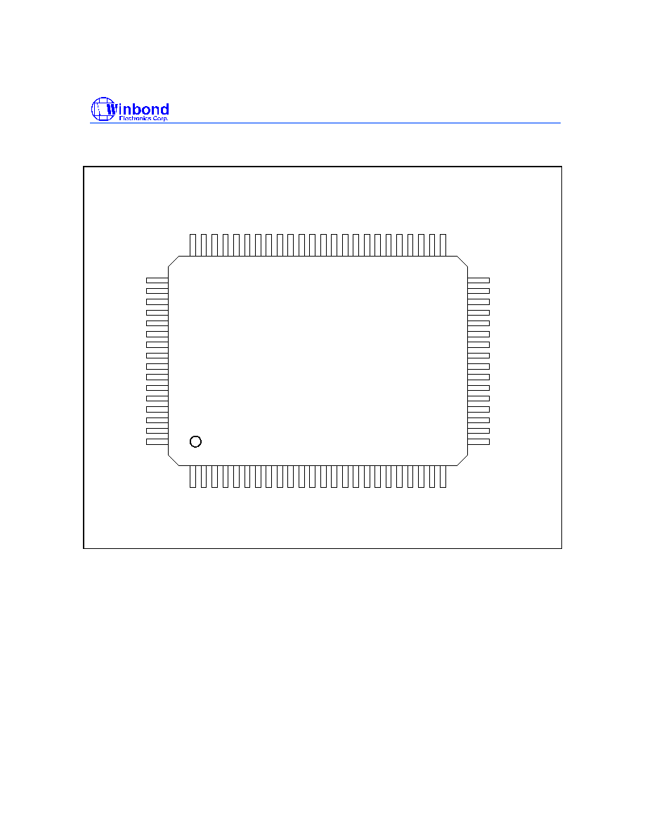
Packaged in 80-pin QFP
W741E260
- 4 -
PIN CONFIGURATION
64 63 62 61 60 59 58 57 56 55 54 53 52 51 50 49 48 47 46
1 2 3 4 5 6 7 8 9 10 11 12 13 14 15 16 17 18 19
33
34
35
36
25
26
27
28
29
30
31
32
65
66
67
68
69
70
71
72
73
74
75
76
77
RD2
RD1
RD0
RC3
RC2
RC1
RC0
RB2
M
F
P
/
R
E
S
X
I
N
1
V
D
D
N
C
D
H
1
D
H
2
V
D
D
3
SEG24
SEG23
SEG22
SEG21
SEG20
SEG19
SEG18
SEG17
SEG16
V
S
S
V
P
P
D
A
T
A
N
C
C
O
M
3
C
O
M
2
C
O
M
1
C
O
M
0
S
E
G
0
S
E
G
1
S
E
G
2
S
E
G
3
S
E
G
4
S
E
G
5
R
E
2
R
E
3
SEG15
SEG14
SEG13
SEG12
RB1
RB0
RB3
S
E
G
3
1
V
D
D
2
V
D
D
1
X
U
O
T
1
R
A
0
20 21 22 23 24
37
38
39
40
45 44 43 42 41
78
79
80
RE1
RE0
RD3
S
E
G
6
S
E
G
7
S
E
G
8
S
E
G
9
S
E
G
1
0
S
E
G
1
1
SEG27
SEG26
SEG25
N
C
N
C
S
E
G
3
0
S
E
G
2
9
S
E
G
2
8
O
X
O
U
T
2
X
I
N
2
R
A
1
N
C
N
C
N
C
M
O
D
E
/
I
N
T
RA2
RA3
W741E260
Publication Release Date: March 1998
- 5 -
Revision A2
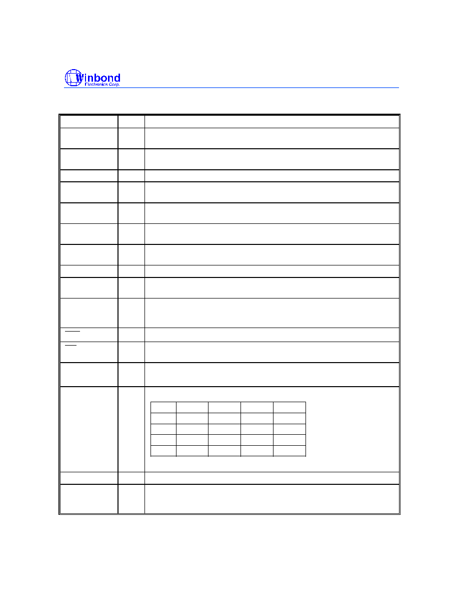
PIN DESCRIPTION
SYMBOL I/O
FUNCTION
XIN1
I
Input pin for main-oscillator.
Connected to crystal or resistor to generate system clock by code option.
XOUT1
O
Output pin for main-oscillator.
Connected to crystal or resistor to generate system clock by code option.
XIN2
I
Input pin for sub-oscillator. Connected to 32.768 KHz crystal.
XOUT2
O
Output pin for sub-oscillator with internal oscillation capacitor. Connected
to 32.768 KHz crystal.
RA0 to RA3
I/O
Input/Output port.
Input/output mode specified by port mode 1 register (PM1).
RB0 to RB3
I/O
Input/Output port.
Input/output mode specified by port mode 2 register (PM2).
RC0 to RC3
I
4-bit port for input only.
Each pin has an independent interrupt capability.
RD0 to RD3
I
4-bit port for input only.
RE0 to RE3
O Output port only.
This port provides high sink current to drive LEDs.
MFP
O
Output pin only.
This pin can output modulating or nonmodulating frequency, or Timer 1
clock output specified by mode register 1 (MR1).
RES
I
System reset pin with pull-high resistor.
INT
I
External interrupt pin with pull-high resistor. This pin is bonding option for
the W741C250 body.
SEG0 to
SEG31
O
LCD segment output pins.
Also can be used as DC output ports specified by option codes.
COM0 to
COM3
O
LCD common signal output pins.
Static
COM0
COM1
COM2
COM3
Used
Not Used
1/2 Duty
Not Used
Not Used
Not Used
Not Used
1/3 Duty
Not Used
1/4 Duty
Used
Used
Used
Used
Used
Used
Used
Used
Used
The LCD alternating frequency can be selected by code option.
DH1, DH2
I
Connection terminals for voltage doubler (halver) capacitor.
V
DD1,
V
DD2,
V
DD3
I
Positive (+) supply voltage terminal.
Refer to Functional Description.