 | –≠–ª–µ–∫—Ç—Ä–æ–Ω–Ω—ã–π –∫–æ–º–ø–æ–Ω–µ–Ω—Ç: W78C354 | –°–∫–∞—á–∞—Ç—å:  PDF PDF  ZIP ZIP |

Preliminary W78C354
MONITOR MICROCONTROLLER
Publication Release Date: October 1996
- 1 -
Revision A1
GENERAL DESCRIPTION
The W78C354 is a high-performance monitor microcontroller that is based on the embedded 80C32
microcontroller core. The W78C354 includes a 16 KB ROM, 512 byte internal data RAM, a 6-bit A/D
converter, two 12-bit and fourteen 8-bit PWM static DACs, one 12-bit and three 8-bit PWM dynamic
DACs, a sync processor, an I
2
C port, a DDC port, a watchdog timer, and glue logic specially designed
for monitor applications.
The W78C354 is suitable for monitors applying VESA DDC1/DDC2B/DDC2B+. This product's high
level of integration and the availability of a one-time programmable (OTP) flash PROM version(the
W78E354) help to reduce unit costs, development costs, and development time.
FEATURES
∑
80C32 MCU core included
∑
20 MHz maximum operating frequency
∑
16 KB ROM for program storage
∑
512 bytes of on-chip data RAM:
-
Lower 256 bytes accessed as in the 80C32
-
Higher 256 bytes accessed as an external data memory via "MOVX @Ri".
∑
One SPI/RS232 port (80C32 standard serial port)
∑
One external interrupt input
∑
Two timers/counters
∑
One 8-bit auto-reload timer for software time base
∑
PWM DACs:
-
Two 12-bit PWM/BRM static DACs
-
Fourteen 8-bit PWM static DACs
-
One 12-bit PWM/BRM dynamic DAC
-
Three 8-bit PWM dynamic DACs
∑
One 6-bit ADC with 4 multiplexed analog inputs
∑
Sync processor:
-
Horizontal & vertical polarity detector
-
Sync separator for composite sync
-
Horizontal & vertical frequency counter
-
Programmable dummy frequency generator
-
Programmable H-clamp pulse output
-
Safe operation area (SOA) output
-
Self-test pattern output
∑
One software I
2
C port
∑
One DDC port (master/slave mode I
2
C, supports DDC1/DDC2B/DDC2B+)
∑
Watchdog timer
∑
Moire cancellation
∑
Two 15 mA output pins for driving LED
∑
Power-low reset
∑
OTP type: W78E354 (16 KB flash PROM)
∑
Three package types:
-
PLCC68 (W78C/E354P), DIP48 (W78C/E354E), DIP40 (W78C/E354)
W78C354
- 2 -
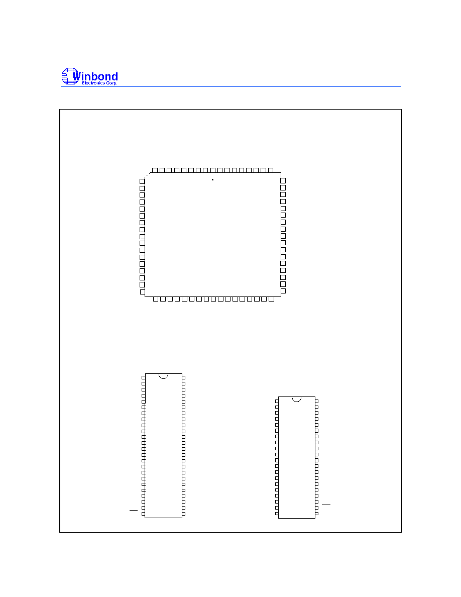
PIN CONFIGURATIONS
W78C/E354P (PLCC68)
SDAC10
10
14
13
12
11
16
15
17
21
20
19
18
23
22
24
26
25
60
56
57
58
59
54
55
53
49
50
51
52
47
48
46
44
45
43
42
41
40
39
38
37
36
35
34
33
32
31
30
29
28
27
61
62
63
64
65
66
67
68
1
2
3
4
5
6
7
8
9
SDAC11
P2.6
P2.7
OSCOUT
OSCIN
VSS
P2.0
P2.1
SDAC12
SDAC13
P2.2
P2.3, STP
P3.4, T0
P3.5, T1
HIN
VIN
H
O
U
T
V
O
U
T
B
S
D
A
C
0
B
S
D
A
C
1
P
3
.
0
,
R
X
D
P
3
.
1
,
T
X
D
/
R
S
T
V
S
S
V
S
S
A
A
D
C
0
A
D
C
1
V
A
A
A
D
C
2
,
P
1
.
6
A
D
C
3
,
P
1
.
7
N
C
P
3
.
2
,
I
N
T
0
P
3
.
6
P4.0
P4.1
P1.0, ISCL
P1.1, ISDA
P1.2, DSCL
DDAC1
DDAC2
BDDAC
SDAC0
P4.2
VPP
P4.3
DDAC0
(Only for W78E354P)
VDD
P1.5, SOA
P1.4, HCLAMP
P1.3, DSDA
P
3
.
3
S
D
A
C
1
S
D
A
C
2
P
4
.
4
S
D
A
C
3
S
D
A
C
4
P
3
.
7
V
D
D
P
4
.
5
P
4
.
6
S
D
A
C
5
S
D
A
C
6
S
D
A
C
7
S
D
A
C
8
S
D
A
C
9
P
2
.
4
P
2
.
5
VDD
1
2
3
4
5
6
7
8
9
10
11
12
13
14
15
16
17
18
19
20
47
48
42
43
44
45
46
38
39
40
41
34
35
36
37
29
30
31
32
33
SDAC4
SDAC3
SDAC2
SDAC1
P3.3
SDAC0
BDDAC
DDAC2
DDAC1
DDAC0
VPP
P1.3, DSDA
P1.4, HCLAMP
P1.5, SOA
P3.2, INT0
P3.6
P1.0, ISCL
P1.1, ISDA
P1.2, DSCL
SDAC5
SDAC7
P2.4, SDAC10
P2.0
OSCOUT
OSCIN
P2.1
P2.2
P2.3, STP
P3.4, T0
P3.5, T1
HIN
HOUT
VIN
VOUT
SDAC6
VDD
1
2
3
4
5
6
7
8
9
10
11
12
13
14
15
16
17
18
19
20
39
40
34
35
36
37
38
30
31
32
33
26
27
28
29
21
22
23
24
25
SDAC4
SDAC3
SDAC2
SDAD1
SDAD0
BDDAC
DDAC0
VPP
P1.5, SOA
P1.4, HCLAMP
P1.3, DSDA
P1.0, ISCL
P1.1, ISDA
P1.2, DSCL
P3.1, TXD
RST
ADC0
NC
P3.2, INT0
SDAC5
SDAC7
P2.4, SDAC10
P2.5, SDAC11
P2.6, SDAC12
P2.7, SDAC13
VSS
P2.0
OSCOUT
OSCIN
P2.1
P2.2
P2.3, STP
HIN
VIN
HOUT
BSDAC0
VOUT
P3.0, RXD
SDAC6
VSSA
ADC0
VAA
NC
BSDAC0
P3.1, TXD
P3.0, RXD
RST
21
22
23
24
28
27
26
25
P2.5, SDAC11
P2.6, SDAC12
P2.7, SDAC13
VSS
(Only for W78E354E)
(Only for W78E354)
W78C/E354E (DIP48)
W78C/E354 (DIP40)
W78C354
Publication Release Date: October 1996
- 3 -
Revision A1
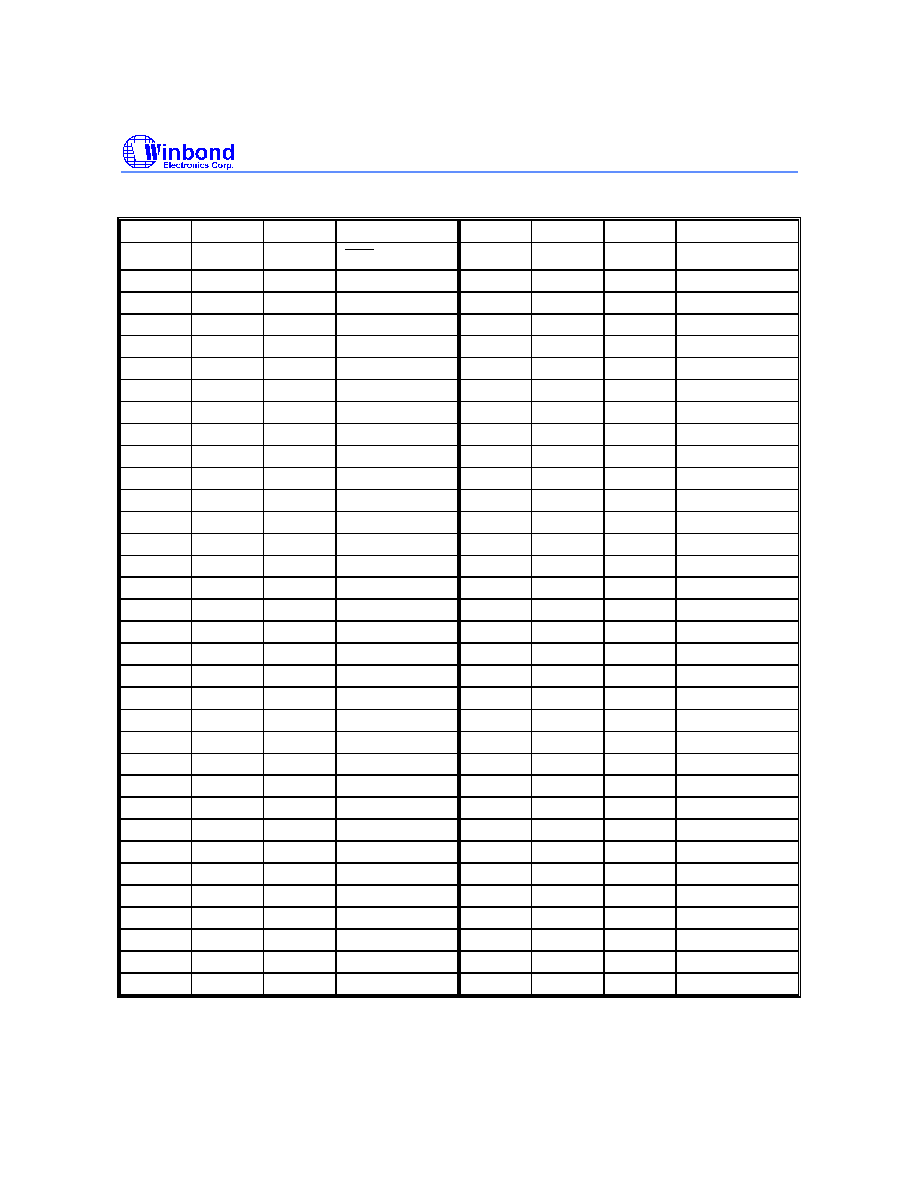
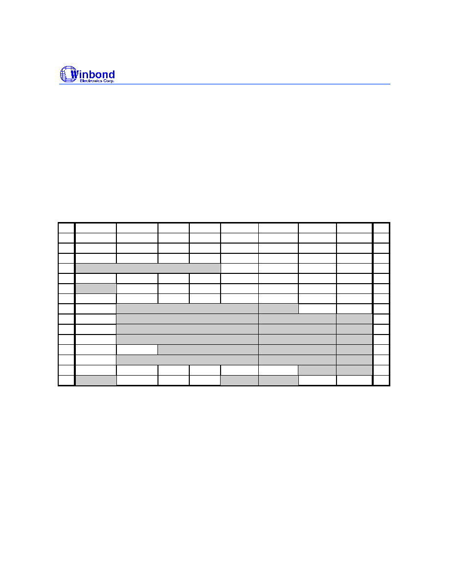
PIN ARRANGEMENT REFERENCE TABLE
DIP-40
DIP-48 PLCC-68
PIN NAME
DIP-40
DIP-48 PLCC-68
PIN NAME
22
24
33
RST
-
-
37
ADC1
15
17
25
HIN
-
-
39
ADC2(P1.6)
16
18
26
VIN
-
-
40
ADC3(P1.7)
17
19
27
HOUT
-
27
38
V
AA
18
20
28
VOUT
-
25
35
V
SSA
35
42
60
SDAC0
11
11
17
P2.0
36
44
62
SDAC1
12
12
18
P2.1
37
45
63
SDAC2
13
13
21
P2.2
38
46
65
SDAC3
14
14
22
P2.3 (STP)
39
47
66
SDAC4
4
4
8
P2.4 (SDAC10)
1
1
3
SDAC5
5
5
9
P2.5 (SDAC11)
2
2
4
SDAC6
6
6
12
P2.6 (SDAC12)
3
3
5
SDAC7
7
7
13
P2.7 (SDAC13)
-
-
6
SDAC8
20
22
31
P3.0 (RXD )
-
-
7
SDAC9
21
23
32
P3.1 (TXD )
-
-
10
SDAC10
25
29
42
P3.2 (INT0)
-
-
11
SDAC11
-
43
61
P3.3
-
-
19
SDAC12
-
15
23
P3.4 (T0)
-
-
20
SDAC13
-
16
24
P3.5 (T1)
19
21
29
BSDAC0
-
30
43
P3.6
-
-
30
BSDAC1
-
-
67
P3.7
40
48
68
V
DD
-
-
44
P4.0
10
10
16
V
SS
-
-
45
P4.1
34
41
59
BDDAC
-
-
53
P4.2
33
38
56
DDAC0
-
-
55
P4.3
-
39
57
DDAC1
-
-
64
P4.4
-
40
58
DDAC2
-
-
1
P4.5
26
31
46
P1.0 (ISCL)
-
-
2
P4.6
27
32
47
P1.1 (ISDA)
24
28
41
NC
28
33
48
P1.2 (DSCL)
32
37
54
V
PP
29
34
49
P1.3 (DSDA)
-
-
52
V
DD
30
35
50
P1.4 (HCLAMP)
-
-
34
V
SS
31
36
51
P1.5 (SOA)
8
8
14
OSCOUT
23
26
36
ADC0
9
9
15
OSCIN

W78C354
- 4 -
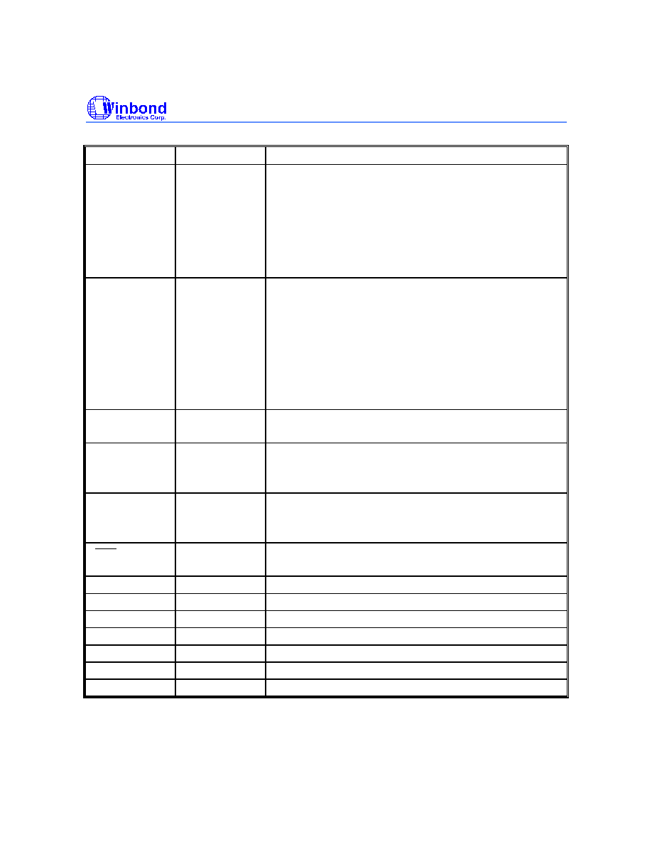
PIN DESCRIPTION
PIN NAME
I/O TYPE
FUNCTION
SDAC0
-
7
O
8-bit PWM static DAC output.
Sink/source current 4 mA/-4 mA.
SDAC8
-
13
O
8-bit PWM static DAC output.
Sink/source current 4 mA/-4 mA.
BSDAC0
-
1
O
12-bit PWM/BRM static DAC output.
Sink/source current 8 mA/-8 mA.
DDAC0
-
2
O
8-bit PWM dynamic DAC output.
Sink/source current 8 mA/-8 mA.
BDDAC
O
12-bit PWM/BRM dynamic DAC output.
Sink/source current 8 mA/-8 mA.
ADC0
ADC1
ADC2 (P1.6)
ADC3 (P1.7)
I
Analog signal input channel to AD converter.
Alternate function:
ADC2: P1.6 input (input only).
ADC3: P1.7 input (input only).
P1.0
-
P1.1
I/O
General purpose I/O.
Open-drain, Sink current 2 mA.
P1.2 (DSCL)
P1.3 (DSDA)
I/O
General purpose I/O.
Open-drain, Sink current 6 mA.
Alternate function:
P1.2: DDC port serial clock DSCL.
P1.3: DDC port serial data DSDA.
P1.4
(HCLAMP)
I/O
General purpose I/O.
Sink/source current 4 mA/-100
µ
A.
Alternate function:
P1.4: HCLAMP (H-clamp pulse) output.
While outputing special function, P1.4 sink/source current is
4 mA/-4 mA.
P1.5 (SOA)
I/O
General purpose O/P.
Sink/source current 4 mA/-4 mA.
Alternate function:
P1.5: SOA (safe operation area) output.
P2.0
-
P2.1
I/O
General purpose I/O.
Sink/source current 15 mA/-100
µ
A.
W78C354
Publication Release Date: October 1996
- 5 -
Revision A1
Pin Description, continued
PIN NAME
I/O TYPE
FUNCTION
P2.2
P2.3
(
STP)
P2.4 (SDAC10)
P2.5 (SDAC11)
P2.6 (SDAC12)
P2.7 (SDAC13)
I/O
General purpose I/O.
Sink/source current 4 mA/-100
µ
A.
Alternate function:
P2.3: STP (Self-Test Pattern) output.
P2.4
-
P2.7: SDAC10
-
13 outputs.
While outputing special function, P2.3
-
P2.7 sink/source
current is 4 mA/-4 mA.
P3.0 (RXD)
P3.1 (TXD)
P3.2 (INT0)
P3.3
P3.4 (T0)
P3.5 (T1)
P3.6
P3.7
I/O
General purpose I/O.
Sink/Source current 2 mA/-100
µ
A.
Alternate function:
P3.0: Serial input port.
P3.1: Serial output port.
P3.2: External interrupt input.
P3.4, P3.5: Timer/counter 0, 1 external inputs.
P4.0
-
P4.6
O
Output port.
Sink/source current 2 mA/-2 mA.
HIN
VIN
I
HIN: Hsync/composite sync input.
VIN: Vsync input.
Schmitt trigger input pin.
HOUT
VOUT
O
HOUT: Hsync output.
VOUT: Vsync output.
Sink/source current 4 mA/-4 mA.
RST
I
Reset the controller (active low).
Schmitt trigger input pin.
OSCOUT
O
Output from inverting oscillator amplifier.
OSCIN
I
Input to inverting oscillator amplifier.
V
PP
I
High voltage supply input for flash PROM.
V
DD
I
Positive power supply for digital circuit, +5V.
V
SS
I
Digital ground.
V
AA
I
Positive power supply for analog circuit, +5V.
V
SSA
I
Analog ground.
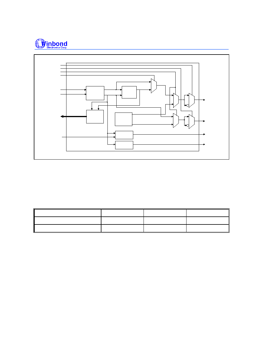
BLOCK DIAGRAM
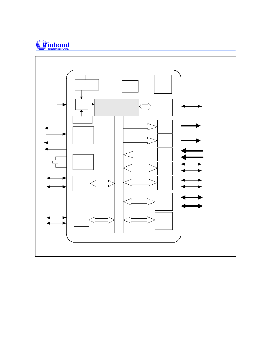
W78C354
- 6 -
CPU
CORE
16K x 8
Mask
ROM
512 x 8
RAM
Power source
Supervisor
Serial
Port
WDT
Timer0
Timer1
TXD
RXD
V
V
RST
SDAC
DDAC
ADC
SDAC0 to 13, BSDAC0 to 1
DDAC0 to 2, BDDAC
ADC0 to 3
ISDA
ISCL
DDC
Port
DSDA
DSCL
Interrupt
Processor
P2
P4
I/O
Port
INT0
T0
T1
Oscillator
Sync.
Processor
HOUT, VOUT
HIN, VIN
HCLAMP
Reset
Circuit
Auto
Reload
Timer
SOA
DD
V
AA
V
,
I
SS
2
C
SSA
W78C354
Publication Release Date: October 1996
- 7 -
Revision A1
FUNCTIONAL DESCRIPTION
The W78C354's core architecture consists of an 80C32 MCU surrounded by various special function
registers, or SFRs (some of these are 80C32 standard registers, while others are newly added; see
Table 1), three general purpose I/O ports (P1, P2, and P3), one output-only port (P4), 256 bytes of
scratchpad RAM, two timer/counters (Timer0 and Timer1) and one 80C32 standard serial port. The
processor supports 109 different instructions (without "MOVX A, @DPTR" and "MOVX @DPTR, A"),
which are all compatible with the 80C32 family instruction set.
There are two major differences between the W78C354 and 80C32. First, the W78C354 cannot
access an external program or data memory. This function is unnecessary, because the W78C354's
16 KB of internal ROM and 512 bytes of on-chip RAM should be enough for most monitor
applications. Second, the W78C354 has a number of new SFRs (see Table 2), which provide more
powerful functions.
Table 1. W78C354 special function registers (SFRs)
F8
FF
F0
+ B
F7
E8
EF
E0
+ ACC
E7
D8
+ S1CON
S1STA
S1DAT
S1ADR
DF
D0
+ PSW
D7
C8
+ CONTREG4
CF
C0
C7
B8
+ IP
SBRM0
SBRM1
PORT4
SOAREG
SOACLR
BF
B0
+ P3
ADC
INTVECT
STATUS
HFCOUNTL
HFCOUNTH
VFCOUNTL
VFCOUNTH
B7
A8
+ IE
SDAC7
SDAC8
SDAC9
SDAC10
SDAC11
SDAC12
SDAC13
AF
A0
+ P2
SDAC0
SDAC1
SDAC2
SDAC3
SDAC4
SDAC5
SDAC6
A7
98
+ SCON
SBUF
BSDAC0
BSDAC1
WDTCLR
DDAC0
DDAC1
DDAC2
9F
90
+ P1
AUTOLOAD
DHREG
DVREG
DDC1
INTMSK
BDDAC
DBRM
97
88
+ TCON
TMOD
TL0
TL1
TH0
TH1
PARAL
PARAH
8F
80
+ CONTREG1
SP
DPL
DPH
CONTREG5
CONTREG2
PCON
87
Notes:
1. SFRs with a "+" are both byte and bit-addressable.
2. The registers in the shaded region are newly added to the 80C32.
A. Memory Address Space
The W78C354 operates in three separate address spaces:
(1) The first (Figure 1-1) is the 16 KB internal program space (0000H
-
3FFFH).
(2) The second (Figure 1-2) is the data memory space, which is 256 bytes in size (0000H
-
00FFH).
The data memory is integrated inside the chip rather than outside the chip, as in a standard
80C32. This data memory space must be accessed by the "MOVX @Ri" instruction.
(3) The third (Figure 1-3) is the same as in the standard 80C32.
W78C354
- 8 -
0000H
3FFFH
00H
FFH
00H
On-Chip
Program Memory
On-Chip
Data Memory
FFH
7FH
80H
(Direct Addressing)
(Direct/Indirect
Addressing)
SFR
Scratchpad
RAM
(Indirect Addressing)
Scratchpad
RAM
(MOVX @Ri)
Figure 1-1
Figure 1-3
Figure 1-2
Figure 1. Memory address space
B. Modified 80C32 SFRs
1. Timer/Counter Control Register (TCON):
BIT
NAME
FUNCTION
TCON.7
TF1
Timer 1 overflow flag.
Set by hardware on timer/counter overflow. Cleared by hardware when
processor vectors to interrupt routine.
TCON.6
TR1
Timer 1 run control bit.
Set/cleared by software to turn timer/counter on or off.
TCON.5
TF0
Timer 0 overflow flag.
Set by hardware on timer/counter overflow. Cleared by hardware when
processor vectors to interrupt routine.
TCON.4
TR0
Timer 0 run control bit.
Set/cleared by software to turn timer/counter on or off.
TCON.3
-
Reserved
TCON.2
-
Reserved
TCON.1
IE0
Interrupt 0 edge flag.
Set by hardware when external interrupt edge detected. Cleared by
hardware when interrupt processed.
TCON.0
IT0
Interrupt 0 type control bit.
Set/cleared by software to specify falling edge/low level triggered external
interrupt.
Note: The registers in the shaded region are modified from the 80C32 SFRs.

W78C354
Publication Release Date: October 1996
- 9 -
Revision A1
2. Power Control Register (PCON):
NAME
FUNCTION
SMOD
Double baud rate bit.
-
Reserved
-
Reserved
-
Reserved
GF1
General-purpose flag bit.
GF0
General-purpose flag bit.
-
Reserved
IDL
Idle mode bit.
Notes:
1. The SFR is not bit-addressable.
2. The registers in the shaded region are modified from the 80C32 SFRs.
3. Interrupt Enable Register (IE):
BIT
NAME
FUNCTION
IE.7
EA
If EA = 0, no interrupt will be acknowledged (disable all interrupts).
If EA = 1, each interrupt source is individually enabled or disabled by
setting or clearing its enable bit.
IE.6
-
(Reserved)
IE.5
*1
Set/clear to enable/disable the DDC port's I
2
C interrupt.
IE.4
ES
Set/clear to enable/disable the serial port 0 interrupt.
IE.3
ET1
Set/clear to enable/disable the Timer 1 overflow interrupt.
IE.2
*1
Set/clear to enable/disable the *2 interrupt.
IE.1
ET0
Set/clear to enable/disable the Timer 0 overflow interrupt.
IE.0
EX0
Set/clear to enable/disable the external interrupt 0.
Notes:
*1. No name for ASSEMBLER, must be used via "IE.x".
".
*2. DSCLINT+ADCINT+TIMEOUT+SOAINT+VEVENT+PARAINT +DDC1INT.

W78C354
- 10 -
4. Interrupt Priority Register (IP)
BIT
NAME
FUNCTION
IP.7
-
(Reserved)
IP.6
-
(Reserved)
IP.5
*1
Define the DDC port's I
2
C interrupt priority level.
If IP.5 = 1, the priority level is higher.
IP.4
PS
Define the serial port interrupt priority level.
If PS = 1, the priority level is higher.
IP.3
PT1
Define the Timer 1 interrupt priority level.
If PT1 = 1, the priority level is higher.
IP.2
*1
Define the *2 priority level.
If IP.2 = 1, the priority level is higher.
IP.1
PT0
Define the Timer 0 interrupt priority level.
If PT0 = 1, the priority level is higher.
IP.0
PX0
Define the external interrupt 0 priority level.
If PX0 = 1, the priority level is higher.
Notes:
*1. No name for ASSEMBLER, must be used via "IP.x".
*2. DSCLINT+ADCINT+TIMEOUT+SOAINT+VEVENT+PARAINT+DDC1INT.
C. Newly Added Special Function Registers
In addition to the 80C32 SFRs, the W78C354 has forty-nine new SFRs in the SFR address space, as
listed in Table 2.
Table 2. New special function registers
REGISTER
ADDRESS
FUNCTION
LENGTH
R/W
TYPE
RESET
CONTENT
1
CONTREG1
80H
Control register 1, bit-addressable
8
R/W
00H
2
CONTREG5
84H
Control register 5
8
R/W
00H
3
CONTREG2
85H
Control register 2
8
W
00H
4
PARAL
8EH
Parabola interrupt generator low byte register
8
W
00H
5
PARAH
8FH
Parabola interrupt generator high byte register
8
W
00H
6
AUTOLOAD
91H
8-bit auto-reload timer register
8
W
00H
7
DHREG
92H
Dummy Hsync frequency generator register
4
W
00H
8
DVREG
93H
Dummy Vsync frequency generator register
8
W
00H
9
DDC1
94H
DDC port's DDC1 data buffer
8
W
00H
10
INTMSK
95H
Interrupt mask register
8
W
00H
11
BDDAC
96H
8-bit PWM register for 12-bit PWM/BRM dynamic DAC
8
W
00H
12
DBRM
97H
4-bit BRM register for 12-bit PWM/BRM dynamic DAC
4
W
00H

W78C354
Publication Release Date: October 1996
- 11 -
Revision A1
Table 2. New special function registers, continued
REGISTER
ADDRESS
FUNCTION
LENGTH
R/W
TYPE
RESET
CONTENT
13
BSDAC0
9AH
8-bit PWM register for 12-bit PWM/BRM Static DAC0
8
W
00H
14
BSDAC1
9BH
8-bit PWM register for 12-bit PWM/BRM Static DAC1
8
W
00H
15
WDTCLR
9CH
Watch-dog timer clear register
-
W
-
16
DDAC0
9DH
8-bit PWM dynamic DAC0 register
8
W
00H
17
DDAC1
9EH
8-bit PWM dynamic DAC1 register
8
W
00H
18
DDAC2
9FH
8-bit PWM dynamic DAC2 register
8
W
00H
19
SDAC0
A1H
8-bit PWM static DAC0 register
8
W
00H
20
SDAC1
A2H
8-bit PWM static DAC1 register
8
W
00H
21
SDAC2
A3H
8-bit PWM static DAC2 register
8
W
00H
22
SDAC3
A4H
8-bit PWM static DAC3 register
8
W
00H
23
SDAC4
A5H
8-bit PWM static DAC4 register
8
W
00H
24
SDAC5
A6H
8-bit PWM static DAC5 register
8
W
00H
25
SDAC6
A7H
8-bit PWM static DAC6 register
8
W
00H
26
SDAC7
A9H
8-bit PWM static DAC7 register
8
W
00H
27
SDAC8
AAH
8-bit PWM static DAC8 register
8
W
00H
28
SDAC9
ABH
8-bit PWM static DAC9 register
8
W
00H
29
SDAC10
ACH
8-bit PWM static DAC10 register
8
W
00H
30
SDAC11
ADH
8-bit PWM static DAC11 register
8
W
00H
31
SDAC12
AEH
8-bit PWM static DAC12 register
8
W
00H
32
SDAC13
AFH
8-bit PWM static DAC13 register
8
W
00H
33
ADC
B1H
6-bit ADC result register
8
R
00H
34
INTVECT
B2H
Interrupt vector register
8
R/W
00H
35
STATUS
B3H
Status register
4
R
00H
36
HFCOUNTL
B4H
Horizontal frequency counter low byte register
8
R
00H
37
HFCOUNTH
B5H
Horizontal frequency counter high byte register
8
R
00H
38
VFCOUNTL
B6H
Vertical frequency counter low byte register
8
R
00H
39
VFCOUNTH
B7H
Vertical frequency counter high byte register
8
R
00H
40
SBRM0
B9H
4-bit BRM register for 12-bit PWM/BRM Static DAC0
4
W
00H
41
SBRM1
BAH
4-bit BRM register for 12-bit PWM/BRM Static DAC1
4
W
00H
42
PORT4
BBH
Output latch register
7
W
00H
43
SOAREG
BCH
Safe operation area register
8
W
00H
44
SOACLR
BDH
Safe operation area clear register
-
W
-
45
CONTREG4
C8H
Control register 4
8
R/W
00H
46
S1CON
D8H
SIO1 port control register
8
R/W
00H
47
S1STA
D9H
SIO1 port status register
8
R
F8H
48
S1DAT
DAH
SIO1 port data register
8
R/W
00H
49
S1ADR
DBH
SIO1 port address register
8
R/W
00H
Notes:
1. "-" means the SFR has no real hardware but only an address.
2. Three SFRs (CONTREG1, CONTREG4, SICON) can be accessed by bit addressing.
D. Status and Control Register Overview
1. STATUS: Status Register
W78C354
- 12 -
BIT
NAME
FUNCTION
0
HP
Hsync polarity. 0: Positive, 1: Negative.
1
VP
Vsync polarity. 0: Positive, 1: Negative.
2
NOH
Set by hardware if no Hsync.
3
NOV
Set by hardware if no Vsync.
2. CONTREG1: Control Register1, Bit-addressable
BIT
NAME
FUNCTION
0
ADCS0
ADC channel select bit 0.
1
ADCS1
ADC channel select bit 1.
2
ENDDC1
Enable/Disable DDC1 mode.
0: Disable DDC1 mode; the pin P1.3/DSDA is accessed data in the
DDC2B/2B+ mode.
1: Enable DDC1 mode ; the pin P1.3/DSDA is output data in the DDC1 mode.
3
HCES
H-Clamp Edge Select.
0: Pin P1.4 will output H-clamp pluse, if the leading edge of Hsync occurs.
1: Pin P1.4 will output H-clamp pluse, if the trailing edge of Hsync occurs.
4
HCWS0
H-Clamp Width Select bit 0.
5
HCWS1
H-Clamp Width Select bit 1.
6
DUMMYEN
Enable/Disable dummy frequency generator.
0: Disable, 1: Enable.
7
ADCSTRT
Start ADC conversion.
0: Stop, 1: Start.
3. CONTREG2: Control Register2
BIT
NAME
FUNCTION
0
ENVS
Enable/Disable Vsync Separator.
0: Disable, 1: Enable.
1
HSPS
Hout Sync Polarity Select.
0: Positive, 1: Negative.
2
VSPS
Vout Sync Polarity Select.
0: Positive, 1: Negative.
3
-
Reserved.
W78C354
Publication Release Date: October 1996
- 13 -
Revision A1
3. CONTREG2: Control Register2, continued
BIT
NAME
FUNCTION
4
EINTES
External INT Edge Select.
0: High-level/rising-edge triggered.
1: Low-level/falling-edge triggered.
5
ENM0
Enable/Disable SDAC0 morie cancel function.
0: Disable, 1: Enable.
6
ENM1
Enable/Disable SDAC1 morie cancel function.
0: Disable, 1: Enable.
7
VDISHC
Disable H-Clamp pulse at the Vsync pulse period. In initial state, it
enables the H-Clamp output.
0: Enable, 1: Disable.
4. CONTREG4: Control Register4, Bit-addressable
BIT
NAME
FUNCTION
0
P24SF
Enable/Disable Port 2.4 Special Function.
P24SF = 0: General I/0 pin.
P24SF = 1 and P2.4 = 0: SDAC10 output.
1
P25SF
Enable/Disable Port 2.5 Special Function.
P25SF = 0: General I/0 pin.
P25SF = 1 and P2.5 = 0: SDAC11 output.
2
P26SF
Enable/Disable Port 2.6 Special Function.
P26SF = 0: General I/0 pin.
P26SF = 1 and P2.6 = 0: SDAC12 output.
3
P27SF
Enable/Disable Port 2.7 Special Function.
P27SF = 0: General I/0 pin.
P27SF = 1 and P2.7 = 0: SDAC13 output.
4
P14SF
Enable/Disable Port 1.4 Special Function.
P14SF = 0: General I/0 pin.
P14SF = 1 and P1.4 = 0: H-Clamp output.
5
P15SF
Enable/Disable Port 1.5 Special Function.
P15SF = 0: General I/0 pin.
P15SF = 1 and P1.5 = 0: SOA output.
6
P23SF
Enable/Disable Port 2.3 Special Function.
P23SF = 0: General I/0 pin.
P23SF = 1 and P2.3 = 0: STP output.
7
INVSTP
Invert Self-Test Pattern.
Note: To let the Px.y output special function, set PxySF and clear Px.y.

W78C354
- 14 -
5. CONTREG5: Control Register5
BIT
NAME
FUNCTION
0
-
Reserved.
1
-
Reserved.
2
-
Reserved.
3
-
Reserved.
4
-
Reserved.
5
HDSEL
HCLAMP Source SELect.
6
DPARAINT
Enable parabola interrupt with dummy signal.
DPARAINT = 0; V dummy signal will generate V
EVENT
interrupt.
DPARAINT = 1; V dummy signal will not generate V
EVENT
interrupt.
7
-
Reserved.
E. I/O Port
The I/O ports available in the W78C354 vary with the package, as shown in the table below:
I/O PORT
68-PIN PLCC
48-PIN DIP
40-PIN DIP
Port 1
6 bits
6 bits
6 bits
Port 2
8 bits
8 bits
8 bits
Port 3
8 bits
7 bits
3 bits
Port 4
7 bits
N.A.
N.A.
P1, P2, and P3 are the SFR latches of ports 1, 2, and 3, respectively. Writing a "1" to a bit of a port
SFR (P1, P2, or P3) causes the corresponding port output pin to switch to high. Writing a "0" causes
the port output pin to switch to low. When a port is used as an input, the external state of the port pin
will be read into the port SFR (i.e., if the external state is low, the corresponding SFR bit will contain a
"0"; if it is high, the bit will contain a "1"). The block diagrams and control registers are shown below.
E-1 Port 1
Besides general purpose I/O functions, port 1 provides the functions shown in the following table.
PINS
SPECIAL FUNCTION
SPECIAL FUNCTION
CONTROL BIT
DESCRIPTION
P1.0
ISCL
-
s/w I
2
C SCL pin
P1.1
ISDA
-
s/w I
2
C SDA pin
P1.2
DSCL
-
DDC port's SCL pin
P1.3
DSDA
-
DDC port's SDA pin
P1.4
HCLAMP
P14SF
H-clamp pulse output
P1.5
SOA
P15SF
SOA output
W78C354
Publication Release Date: October 1996
- 15 -
Revision A1
CL
D
Q
Q
Int.Bus
Write to
Latch
Read
Latch
Read
Pin
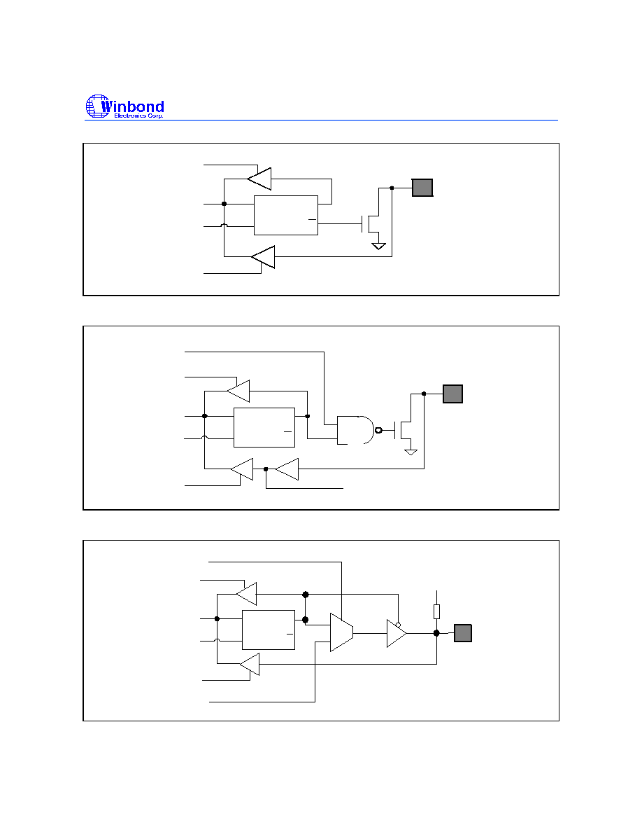
P1.0/P1.1
Figure 2-1. P1.0/P1.1 architecture
CL
D
Q
Q
Int.Bus
Write to
Latch
SCL output/
Read
Latch
SCL input
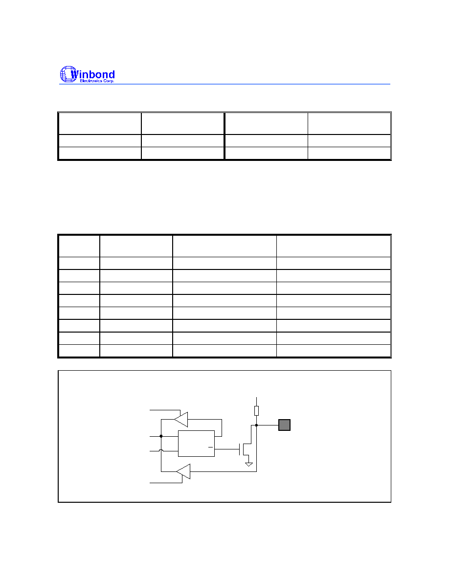
P1.2/P1.3
Read
Pin
SDA output
/
SDA
input
Figure 2-2. P1.2/P1.3 architecture
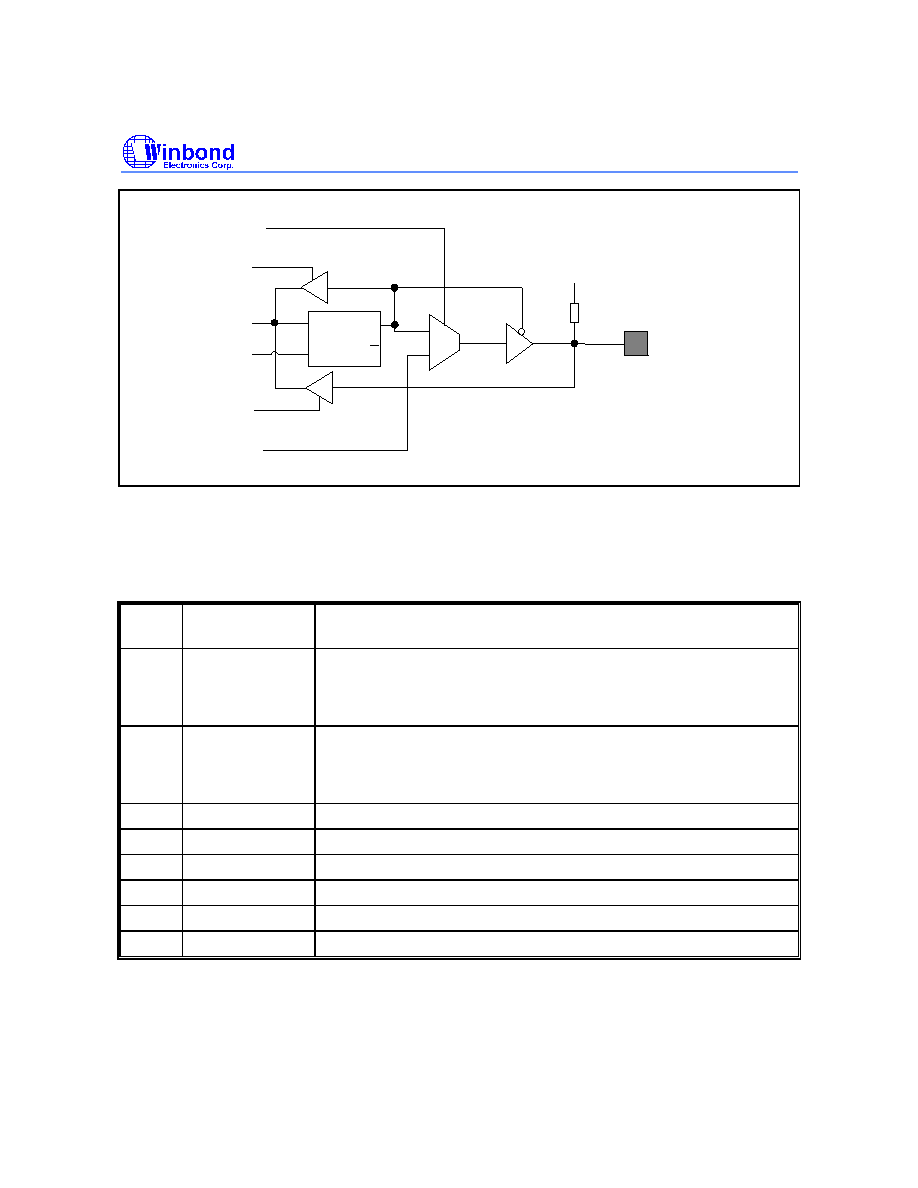
CL
D
Q
Q
Int.Bus
Write to
Latch
Hclamp/SOA
Read
Latch
Read
Pin
P1.4/P1.5
Vcc
Internal
Pullup
P14SF/P15SF
0
1
Figure 2-3. P1.4/P1.5 architecture
W78C354
- 16 -
To use the alternate function H-clamp pulse (SOA output) of P1.4 (P1.5), bit P14SF (P15SF) of the
SFR CONTREG4 must be set to "1" and a "0" must be written to P1.4 (P1.5).
CONDITION OF P14SF
PORT 1.4 I/O PIN
FUNCTION
CONDITION OF P14SF
PORT 1.5 I/O PIN
FUNCTION
P14SF = 0
General I/O pin
P15SF = 0
General output pin
P14SF = 1 & P1.4 = 0
Hclamp pulse output
P15SF = 1 & P1.5 = 0
SOA output
E-2 Port 2
Port 2.0
-
2.2 are used for general purpose I/O functions only, whereas 2.3
-
2.7 have alternate
functions, as shown below. In the 40-pin and 48-pin DIP packages, SDAC10
-
13 have no dedicated
output pins, but share pins with P2.4
-
P2.7. Each pin can be used as an I/O or SDAC output pin by bit-
addressing SFR CONTREG4. When a pin is used for a special function, the output source current is 4
mA. Otherwise, the source current is 100
µ
A.
PINS
SPECIAL
FUNCTION
SPECIAL FUNCTION
CONTROL BIT
DESCRIPTION
P2.0
-
-
-
P2.1
-
-
-
P2.2
-
-
-
P2.3
STP
P23SF
Self -test pattern output
P2.4
SDAC10
P24SF
SDAC10 PWM output
P2.5
SDAC11
P25SF
SDAC11 PWM output
P2.6
SDAC12
P26SF
SDAC12 PWM output
P2.7
SDAC13
P27SF
SDAC13 PWM output
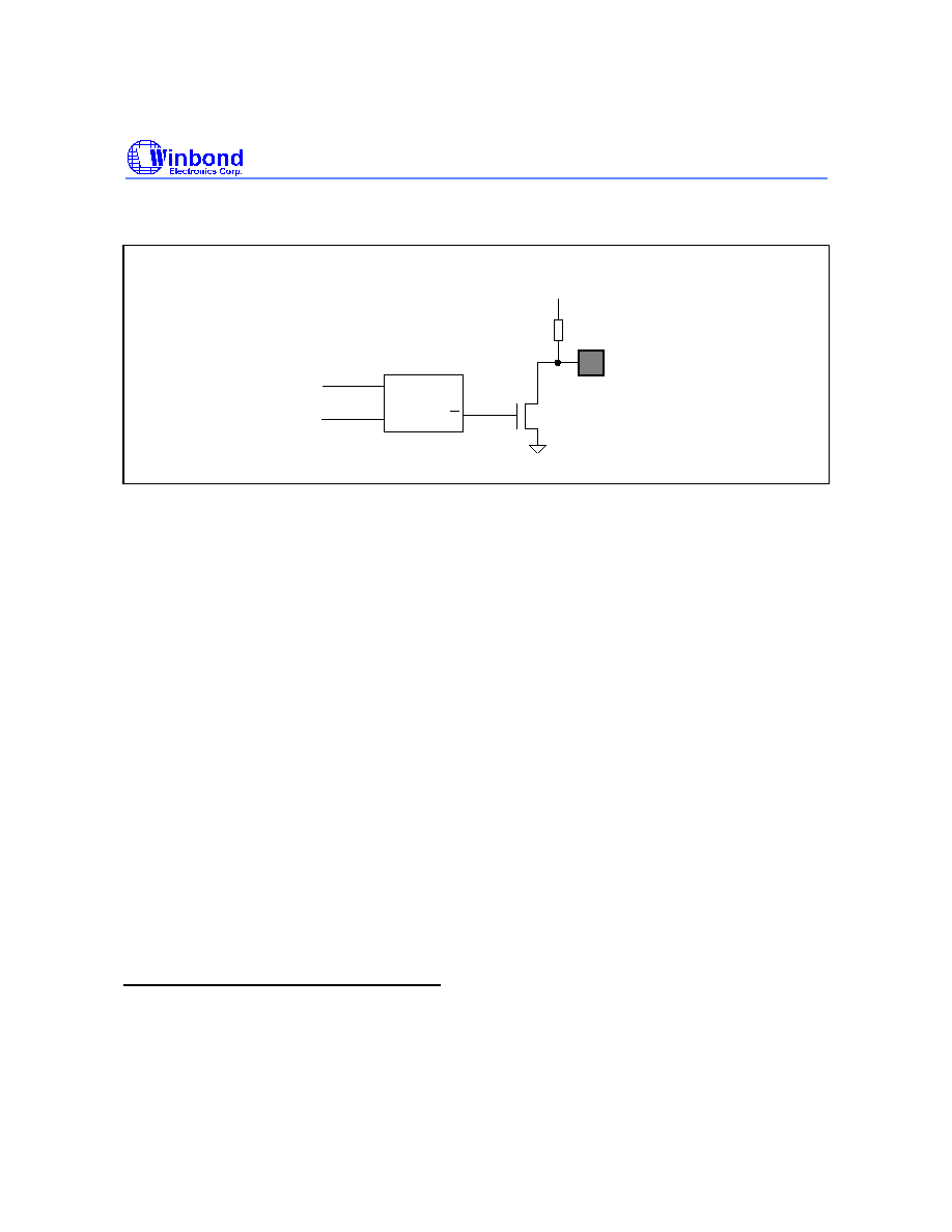
CL
D
Q
Q
Int.Bus
Write to
Latch
Read
Latch
Read
Pin
P2.0 to P2.2
Vcc
Internal
Pullup
Figure 3-1. P2.0 to P2.2 architecture
W78C354
Publication Release Date: October 1996
- 17 -
Revision A1
SDAC
CL
D
Q
Q
Int.Bus
Write to
Latch
Read
Latch
Read
Pin
P2.n/SDAC
Vcc
Internal
Pullup
P2nSF
0
1
n+6
n+6
Figure 3-2. P2.4 to P2.7 architecture (where n = 4
-
7)
E-3 Port 3
The architecture of Port 3 is similar to that of P2.0. There are no special function control bits for these
bits; the output latch of the bits must be set to high to enable the special functions.
PINS
SPECIAL
FUNCTION
DESCRIPTION
P3.0
SPID/RXD
If serial port is in mode 0, the pin works as the data line of the SPI
port.
If serial port is in mode 1, 2, or 3, the pin works as the RXD of the
80C32 standard.
P3.1
SPIC/TXD
If serial port is in mode 0, the pin works as the clock line of the SPI
port.
If serial port is in mode 1, 2, or 3, the pin works as the TXD of the
80C32 standard.
P3.2
INT0
External Interrupt input
P3.3
-
P3.4
T0
Counter/Timer 0 input
P3.5
T1
Counter/Timer 1 input
P3.6
-
P3.7
-
W78C354
- 18 -
E-4 Port 4
Port 4 is an output port. The W78C354 can write data to this port using SFR PORT4.
CL
D
Q
Q
Int.Bus
Write to
Latch
Vcc
Internal
Pullup
P4.0 to P4.6
Figure 4-1. Port 4 architecture
F. SPI (Synchronous Peripheral Interface) and RS232 Port
∑
P3.0 (RXD) and P3.1 (TXD) can be used as an SPI port (serial port mode 0 on the standard 80C32)
or an RS232 port (serial port mode 1, 2, or 3 on the standard 80C32).
∑
The SPI port can be used to communicate with an OSD chip, DAC, and so on.
∑
The RS232 port can be used to communicate with an auto-alignment system, by using a 18.432
MHz crystal. Maximum baud rate is 19200 bps.
G. DDC Port (Display Data Channel Port)
The DDC port is composed of the SIO1 and DDC1 ports, and the SIO1 port shares the DSDA pin with
the DDC1 port (as shown in Figure 5). The DDC port is designed to support DDC1, DDC2B, and
DDC2B+ applications.
G-1 SIO1 Port
SIO1 is an I
2
C serial I/O port. SIO1 provides a serial interface that meets the I
2
C bus specification
and supports all transfer modes from and to the I
2
C bus. The SIO1 port handles byte transfers
autonomously.
The W78C354 interfaces to the SIO1 port through the following four special function registers:
S1CON (SIO1 control register), S1STA (SIO1 status register), S1DAT (SIO1 data register), and
S1ADR (SIO1 address register). The SIO1 port interfaces to the DDC I
2
C bus via two pins: P1.2 /
DSCL (DDC I
2
C serial clock line) and P1.3/DSDA (DDC I
2
C serial data line). The output latches of
P1.2 and P1.3 must be set to "1" in order to enable the SIO1 port. For more detailed information,
refer to the description of the Philips I
2
C bus.
G-1.1 S1ADR (SIO1 Address Register) (DAH)
The W78C354 can read from and write to this 8-bit newly added SFR S1ADR. When the the SIO1
port is in a master mode, the content of this register is irrelevant. In slave mode, the seven most
significant bits must be loaded with the address that owns the slave.

W78C354
Publication Release Date: October 1996
- 19 -
Revision A1
7
6
5
4
3
2
1
0
S1ADR
X
X
X
X
X
X
X
-
|--------------- Address that owns slave ---------------|
G-1.2 S1DAT (SIO1 Data Register) (DBH)
This register contains a byte of serial data that is waiting to be transmitted or has just been received.
When the W78C354 is not performing a shifting operation, data can be read from or written to SFR
S1DAT. Data in the S1DAT remain stable as long as SI is set. Data in the S1DAT are shifted from the
most significant bit to the least significant bit, and while data are being shifted out, data on the bus
are simultaneously being shifted in. S1DAT always contains the last data byte present on the bus.
Thus, if arbitration is lost, the transition from master transmitter to slave receiver is made with the
correct data in S1DAT.
7
6
5
4
3
2
1
0
S1DAT
SD7
SD6
SD5
SD4
SD3
SD2
SD1
SD0
MSB
LSB
Eight bits of data in the S1DAT are shifted out or in, followed by an acknowledge bit. The
acknowledge (ACK) bit is controlled by the SIO1 port hardware and cannot be accessed by the
W78C354. Serial data are shifted through the ACK flag into S1DAT on the rising edges of the serial
clock pulses on the SCL line and are shifted out from the S1DAT on the falling edges of the SCL
clock pulse. When a byte has been shifted into the S1DAT, the serial data are available in S1DAT,
and the acknowledge bit is returned by the control logic during the ninth clock pulse.
G-1.3 S1CON (SIO1 Control Register) (D8H)
The newly added SFR S1CON can be read or written by the programmer. Two bits (SI and STO) are
affected by the SIO1 port hardware. When a serial interrupt is requested, the bit SI is automatically
set, and when a stop condition is present on the bus, the bit STO is cleared. The bit STO is also
cleared when ENS1 = "0."
7
6
5
4
3
2
1
0
S1CON
CR2 ENS1 STA
STO
SI
AA
CR1
CR0
G-1.4 ENS1 (SIO1 Enable Bit)
When the bit ENS1 is "0," the SDA and SCL outputs are in a high impedance state, the SIO1 port is
in the "not addressed" slave mode, and no other bits are affected, except that the bit STO in S1CON
is forced to "0." P1.2 and P1.3 may be used as open drain I/O pins.
When ENS1 is "1," SIO1 is enabled. The P1.2 and P1.3 pins must be set to high.

W78C354
- 20 -
G-1.5 STA (SIO1 Start Flag)
When STA is "1," the SIO port will enter the master mode. After the SIO1 port checks the status of
the I
2
C bus, it will generate a start condition if the bus is free. If the bus is not free, the SIO1 port will
wait for a stop condition and then generate a start condition after a delay.
If the bit STA is set while SIO1 is already in master mode and one or more bytes are to be
transmitted or received, SIO1 will transmit a repeated start condition. The bit STA may also be set
when SIO1 is an addressed slave.
When STA is "0," no start condition or repeated start condition will be generated.
G-1.6 STO (SIO1 Stop Flag)
When STO is "1," the SIO1 port is in the master mode and a stop condition is transmitted to the I
2
C
bus. When the stop condition is detected on the bus, the SIO1 port will clear STO. In the slave mode,
STO may be set to recover from an error condition. In this case, no stop condition exists the I
2
C bus,
but the SIO1 port behaves as if a stop condition has been received and switches to the defined "not
addressed" slave receiver mode. STO is automatically cleared by hardware.
G-1.7 SI (SIO1 Serial Interrupt Flag)
When SI is "1," if the bits EA and ES1 (in the IE register) are also set, then once a serial interrupt is
requested, SI will automatically be set by hardware. The only state that does not cause SI to be set is
state F8H, which indicates that no relevant state information is available.
When the bit SI is "1," the low period of the serial clock on the SCL pin is extended, and the serial
transfer is suspended. SI must be reset by software.
When SI is "0," no serial interrupt is requested, so there is no extension of the serial clock on the SCL
pin.
G-1.8 AA (SIO1 Assert Acknowledge Flag)
If AA is "1," an acknowledge signal (low level to the SDA pin) will be generated during the
acknowledge clock pulse on the SCL pin when:
(1) The address owning the slave has been received.
(2) A data byte has been received while the SIO1 port is in the master receiver mode.
(3) A data byte has been received while the SIO1 port is in the addressed slave receiver mode.
If the bit AA is "0," a not acknowledge signal (high level to the SDA pin) will be generated during the
acknowledge clock pulse on the SCL pin when:
(1) A data byte has been received while the SIO1 port is in the master receiver mode
(2) A data byte has been received while the SIO1 port is in the addressed slave receiver mode.
G-1.9 CR0, CR1 and CR2 (SIO1 Clock Rate Bits)
When the SIO1 port is in master mode, these three bits will determine the serial clock frequency (see
the table below). These bits are unimportant when SIO1 is in slave mode. In slave mode, the SIO1
port will automatically synchronize with any clock frequency up to 100 KHz on the I
2
C bus.
W78C354
Publication Release Date: October 1996
- 21 -
Revision A1
Table 3. Serial clock rates
BIT FREQUENCY (KHz) AT THE SCL
PIN
CR2
CR1
CR0
16 MHz
18.432 MHz
20 MHz
FORMULA
0
0
0
63
72
78
F
OSC
/256
0
0
1
71
82
89
F
OSC
/224
0
1
0
83
96
-
F
OSC
/192
0
1
1
100
-
-
F
OSC
/160
1
0
0
17
19
20
F
OSC
/960
1
0
1
-
-
-
F
OSC
/120
1
1
0
-
-
-
F
OSC
/60
G-1.10 S1STA (SIO1 Status Register) (D9H)
The newly added SFR S1STA is an 8-bit read-only register. The three least significant bits are always
zero. The five most significant bits contain the status code. There are 26 possibile status codes.
When the S1STA contains F8H, no serial interrupt is requested. All other the S1STA values
correspond to defined SIO1 states (refer to the Philips specification for the I
2
C bus). When each of
these states is entered, a status interrupt is requested (SI = 1). A valid status code is present in the
S1STA one machine cycle after the bit SI is set by hardware and is still present one machine cycle
after the bit SI has been reset by software.
G-2 DDC1 Port
DDC1 is a serial output port that supports DDC1 communication. After the DDC1 control circuit loads
the next data byte from the data buffer to the shift register and generates a DDC1INT signal to the
CPU, eight data bits and one zero (for the "acknowledge" signal) are shifted out to the DSDA pin
sequentially on each rising edge of the VIN signal. In the interrupt service routine, the W78C354
should fetch the next byte of EDID data and write it to SFR DDC1. If the bit ENDDC1 of SFR
CONTREG1 is cleared to zero, the shift register is stopped, and the DSDA output is kept high.
∑
One DDC1 port to support DDC1; ENDDC1 must be set to 1.
∑
One SIO1 port support DDC2B/2B+; ENDDC1 must be set to 0.

W78C354
- 22 -
DDC1 port
ENDDC1
P1.2/DSCL
P1.3/DSDA
SIO1 port
Support DDC2B/2B+
Support DDC1
SCL
SDA
SDA
SCL
0
1
V
SDA
IN
SCL
IN
OUT
IN
OUT
Figure 5. DDC port
H. Interrupts
The W78C354 has six interrupt sources. Five (except INT1, at vector address 0013H) are identical to
those in the 80C51 series, while the sixth (at vector address 002BH) is newly added. All the interrupt
sources and the corresponding interrupt vector addresses for the W78C354 are described in the
following table:
SOURCE
VECTOR
ADDRESS
DESCRIPTION
PRIORITY
IE0
0003H
External interrupt 0 (same as the 80C31)
Highest
TF0
000BH
Timer 0 overflow interrupt (same as the 80C31)
*1
0013H
Replaces INT1 of the 80C31
TF1
001BH
Timer 1 overflow interrupt (same as the 80C31)
RI+TI
0023H
Serial port interrupt (same as the 80C31)
*2
002BH
New (similar to TF2+EXF2 in the 80C32)
Lowest
Notes:
*1. DSCLINT+ADCINT+TIMEOUT+SOAINT+VEVENT+PARAINT+DDC1INT.
*2. This is the interrupt generated by the I
2
C in the DDC port.
W78C354
Publication Release Date: October 1996
- 23 -
Revision A1
H-1. Interrupt at Vector Address 0013H
The interrupt at vector address 0013H is driven by another seven different sources, which are a high-
to-low transition on the DSCL pin of the DDC port, the A/D converter, the auto-reload timer, the SOA
output, Vsync frequencg event, the parabola interrupt generator, and DDC1 in the DDC port. These
sources are described below.
(1) DSCLINT:
Interrupt generated when DSCL-pin changes from high to low and stays high for 12 clock periods.
Once DDCLINT interrupt is received, the programmer should disable DDC1 port by writing "0" to the
bit ENDDC1 of SFR CONTREG1.
16 MHz
18.432 MHz
20 MHz
DSCL low
750 nS
651 nS
600 nS
(2) ADCINT:
Refer to section K for a description of the ADC.
(3) TIMEOUT:
Refer to section I for a description of the auto-reload timer.
(4) SOAINT:
When an SOA condition occurs, SOAINT will interrupt the CPU to perform the necessary operations.
Refer to section M-6 for a description of the SOA function.
(5) VEVENT:
When the V retrace signal is detected or the V-frequency counter overflows, which means that the
Vsync frequency is so low that it is out of range, the W78C354 will generate the VEVENT interrupt. In
the interrupt service routine, the programmer can check bit 3 (NOV) of SFR STATUS to determine
whether the V frequency is out of range. If NOV = 1, the software should go to DPMS process. If NOV
= 0, the software can read the HFCOUNT and VFCOUNT registers, and the bits HP and VP of
STATUS will determine the preset mode of the incoming frequency. Refer to section M for a
description of the sync processor.
(6) PARAINT:
The parabola interrupt generator is used to generate interrupts to the W78C354 for loading the
parabola waveform data to dynamic DACs. The software should calculate the value of the PARAH
and PARAL registers by (Vcount
◊
16)
˜
section number. Refer to section J for a description of the
parabola interrupt generator.
(7) DDC1INT:
Refer to section G-2 for a description of the DDC1 operation.
Programmer must read SFR INTVECT (bits 0
-
6) to determine the source of the interrupt request.
These seven interrupt sources can be enabled individually by setting SFR INTMSK (bits 0
-
6). The
newly added interrupt at vector address 002BH is driven by the I
2
C circuit in the DDC port.
The interrupt enable control bits for the two interrupts at 0013H and 002BH are IE.2 and IE.5 in the IE
register, respectively. The interrupt priority control bits are IP.2 and IP.5 in the IP register. The
interrupts can be disabled by clearing IE.7 (disable all interrupts). For example, the programmer can
enable the A/D converter interrupt by the "MOV INTMSK, #00000010B" instruction. When the

W78C354
- 24 -
converter is completed, the interrupt will be generated and the bit ADCINT in the INTVECT will
automatically be set. To clear the bit ADCINT to receive the next interrupt, the programmer can use
the "MOV INTVECT, #00000010B" instruction. See Figure 6.
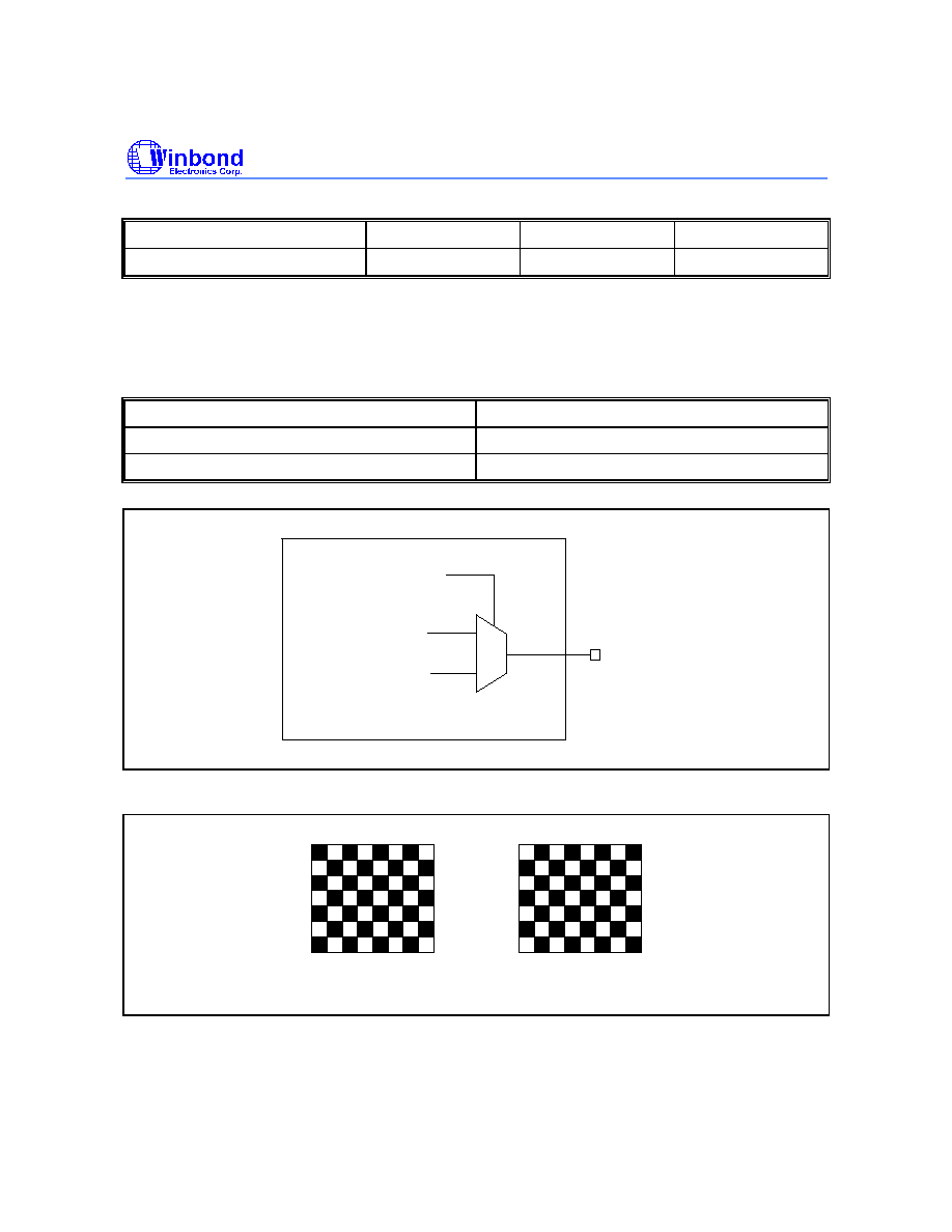
I C in DDC port
2
OR
TIMEOUT source
DSCLINT source
ADCINT source
PARAINT source
VEVENT source
DDC1INT source
IE0
TF0
TF1
RI+TI
INTMSK
IE
0013H
001BH
0023H
002BH
000BH
0003H
IE.3
IE.4
IE.5
IE.2
IE.1
IE.0
IE.7
IP
IP.0
IP.1
IP.2
IP.3
IP.4
IP.5
Vector Address
High Priority
Low Priority
Interrupt Polling
Sequence
SOAINT source
TIMEOUT
DSCLINT
ADCINT
PARAINT
VEVENT
DDC1INT
SOAINT
INTVECT
Bit 0
Bit 1
Bit 2
Bit 4
Bit 3
Bit 6
Bit 5
Figure 6. Interrupt block diagram
H-2. Newly Added External Interrupt 0 Function (INT0)
INT0 can be set to be falling-edge or low-level active by setting/clearing the IT0 bit in TCON. If
programmers wish to use a rising-edge or high-level signal as interrupt on the pin INT0, INT0 can also
be activated by setting/clearing the EINTES bit in SFR CONTREG2 (see Figure 7). In other words,
there are four trigger types for INT0 (falling-edge, low-level, rising-edge. and high-level). In the initial
state, INT0 will be triggered by a rising-edge or high-level signal.
0
1
EINTES
IE0
IT0
1
INT0
(P3.2)
0
Figure 7. External interrupt 0

W78C354
Publication Release Date: October 1996
- 25 -
Revision A1
INTVECT
: Interrupt Vector Register (B2H)
BIT
NAME
FUNCTION
0
DSCLINT
Set by hardware when DSCL is toggled low.
1
ADCINT
Set by hardware when ADC conversion is completed.
2
TIMEOUT
Set by hardware when autoload timer times out.
3
SOAINT
Set by hardware when SOA is high.
4
VEVENT
Set by hardware when Vsync or vertical frequency counter times
out.
5
PARAINT
Set by hardware when parabola interrupt generator times out.
6
DDC1INT
Set by hardwrae when DDC port functions in the DDC1 mode .
7
-
Reserved.
Notes:
1. Each of the above interrupt flags will be set by hardware when the corresponding interrupt source is masked by writing a "1"
to the the INTMSK register.
2. To clear the interrupt flag, write a "1" (not "0") to the corresponding bit.
INTMSK
: Interrupt Mask Register (95H)
BIT
NAME
FUNCTION
0
DSCLINT
Enable/Disable DSCLINT interrupt.
0: Disable, 1: Enable.
1
ADCINT
Enable/Disable ADCINT interrupt.
0: Disable, 1: Enable.
2
TIMEOUT
Enable/Disable TIMEOUT interrupt.
0: Disable, 1: Enable.
3
SOAINT
Enable/Disable SOAINT interrupt.
0: Disable, 1: Enable.
4
VEVENT
Enable/Disable VEVENT interrupt.
0: Disable, 1: Enable.
5
PARAINT
Enable/Disable PARAINT interrupt.
0: Disable, 1: Enable.
6
DDC1INT
Enable/Disable DDC1INT interrupt.
0: Disable, 1: Enable.
7
-
Reserved
W78C354
- 26 -
I. Timer/Counter
The W78C354 has two 16-bit timer/counters, Timer/counter 0 and Timer/counter 1, which are
identical with those on the standard 80C32, and one 8-bit auto-reload timer. Once the "MOV
AUTOLOAD, #data" instruction is executed, the auto-reload timer will load the specified data and
start to count. If the TIMEOUT bit in INTMSK is set, the auto-reload timer will periodically generate an
interrupt to the CPU.
The auto-reload timer interval is programmable:
∑
Minimum timer interval = 1/(F
CLOCK
°“
1024)
∑
Desired timer interval = Minimum interval
◊
[(preset value of the AUTOLOAD)+1]
∑
Maximum timer interval = Minimum interval
◊
255
∑
AUTOLOAD: 8-bit auto-reload timer register which stores preset value.
16 MHz
18.432 MHz
20 MHz
Minimum Interval
64
µ
S
55
µ
S
51.2
µ
S
Maximum Interval
16.3 mS
14.2 mS
13.1 mS
J. Parabola Interrupt Generator
The parabola interrupt generator is a 16-bit binary count-up auto-reload timer that is used to generate
the parabola interrupt to the W78C354 for loading parabola waveform data to dynamic DACs. It
periodically generates an interrupt by setting the PARAINT bit in INTMSK, if the "MOV PARAL, #Low
byte data" and "MOV PARAH, #High byte data" instructions are executed.
The parabola interrupt generator period is programmable:
Time base = 1/F
CLOCK
∑
Desired interrupt period = Time base
◊
{[preset value of the (PARAH, PARAL)]+1}
∑
Maximum period = Time base
◊
65535
∑
PARAL: Parabola interrupt generator register that stores low byte preset value
∑
PARAH: Parabola interrupt generator register that stores high byte preset value
K. 6-bit A/D Converter
The 6-bit analog-to-digital converter uses the successive approximation method to convert one of the
four analog input channels into a digital data value. The A/D converter resolution is
±
1 LSB, and the
conversion time is 100 usec. The result is read from SFR ADC.
Bit-pairs (ADCS1, ADCS2) in SFR CONTREG1 are used to select one of the four channels as the
analog input (see Table 3). Conversion is started by setting the bit ADCSTRT in CONTREG1 by
software. When the A/D conversion is completed, the ADCSTRT bit is automatically cleared by
hardware to stop the A/D converter's operation, and the ADCINT bit in INTVECT is set by hardware at
the same time. To enable the A/D converter interrupt, set the ADCINT bit in INTMSK.
Table 4. Select A/D converter channel
(ADCS1, ADCS0)
(0, 0)
(0, 1)
(1, 0)
(1, 1)
Selected channel
ADC0
ADC1
ADC2
ADC3

W78C354
Publication Release Date: October 1996
- 27 -
Revision A1
L. PWM DACs
There are two 12-bit and fourteen 8-bit PWM static DACs and one 12-bit and three 8-bit PWM
dynamic DACs on this chip. The number of the PWM outputs is different with the package.
68-PIN PLCC
48-PIN DIP
40-PIN DIP
8-bit SDAC
14
8 + 4*
8 + 4*
12-bit SDAC
2
1
1
8-bit DDAC
3
3
1
12-bit DDAC
1
1
1
Note : 4* : the SDAC
S
share with P2.4~P2.7
L-1.1 14-channel 8-bit PWM Static DAC
The static DACs (SDAC0 to 13) are used to generate DC voltage control (0 to 5V) by an RC circuit,
as shown in Figure 8, and to execute the "MOV SDACn, #Value" instruction. There are 14 registers,
corresponding to the 14 channels of 8-bit PWM output. The unused PWM channel can be used as an
output pin, since 0 or 5V can be obtained from the pin.
∑
Duty cycle of the PWM output = Preset value of SDACn
°“
255, where n = 0 to 13
∑
DC voltage after low-pass filter = V
CC
◊
duty cycle
∑
SDAC0
-
SDAC13: 8-bit PWM static DAC registers storing preset values
PRESET VALUE
DUTY CYCLE
DC VOLTAGE
0
0/255
0V
1
1/255
1/255
◊
5V
n
n/255
n/255
◊
5V
255
255/255
+5V
∑
PWM frequency F
PWM
= F
CLOCK
°“
255
Fclock
16 MHz
18.432 MHz
20 MHz
F
PWM
62.745 KHz
72.282 KHz
78.431 KHz
T
PWM
15.94
µ
S
13.83
µ
S
12.75
µ
S

W78C354
- 28 -
8/12bit SDAC
Low-pass filter
V
OUTPUT
R
C
W78C354
Figure 8. SDAC application circuit (where T = RC, V
OUTPUT
= V
CC
◊
n/255, if T >> T
PWM
)
When bit ENM0 of SFR CONTREG2 is set to high, SDAC0 will output PWM in one frame and then
keep low for the next frame. Thus SDAC0 can be used for H moire cancellation. SDAC1 can also be
configured with the same operation for V moire cancellation by setting bit ENM1. The application
circuit is shown below.
SDAC0
(H-moire)
SDACx
(H-phase)
H-phase
Control
Circuit
Figure 9. Moire application circuit
L-1.2 Two-channel 12-bit PWM/BRM Static DAC
The two 12-bit PWM/BRM outputs (BSDAC0,1) are composed of an 8-bit PWM and a 4-bit BRM (bit
rate multiplier). The value of the 4-bit BRMs (SFRs SBRM0, 1) determine to which positions one
clock pulse will be added in every 16 PWM outputs of 12-bit PWM/BRM static DAC0,1. When the
"MOV BSDACn, #value" or "MOV SBRMn, #value" instruction is executed, the related output pin will
output the PWM waveform needed by the user. The 12-bit PWM/BRM frequency is the same as that
of the 8-bit PWM output.
VALUE OF SBRM0 OR SBRM1
(BIT3 BIT2 BIT1 BIT0)
ONE CLOCK PLUSE INCREMENTED IN THE N-TH
OUTPUT EVERY 16 PWM OUTPUTS
0000
None
0001
n = 8
0010
n = 4, 12
0100
n = 2, 6, 10, 14
1000
n = 1, 3, 5, 7, 9, 11, 13, 15
W78C354
Publication Release Date: October 1996
- 29 -
Revision A1
In the following table, in the positions marked with an "
§
" one clock pulse will be added to every 16
PWM outputs.
SBRM0,
PWM/BRM OUTPUT CYCLE
SBRM1
0
1
2
3
4
5
6
7
8
9
10
11
12
13
14
15
0000
-
-
-
-
-
-
-
-
-
-
-
-
-
-
-
-
0001
-
-
-
-
-
-
-
-
§
-
-
-
-
-
-
-
0010
-
-
-
-
§
-
-
-
-
-
-
-
§
-
-
-
0011
-
-
-
-
§
-
-
-
§
-
-
-
§
-
-
-
0100
-
-
§
-
-
-
§
-
-
-
§
-
-
-
§
-
0101
-
-
§
-
-
-
§
-
§
-
§
-
-
-
§
-
0110
-
-
§
-
§
-
§
-
-
-
§
-
§
-
§
-
0111
-
-
§
-
§
-
§
-
§
-
§
-
§
-
§
-
1000
-
§
-
§
-
§
-
§
-
§
-
§
-
§
-
§
1001
-
§
-
§
-
§
-
§
§
§
-
§
-
§
-
§
1010
-
§
-
§
§
§
-
§
-
§
-
§
§
§
-
§
1011
-
§
-
§
§
§
-
§
§
§
-
§
§
§
-
§
1100
-
§
§
§
-
§
§
§
-
§
§
§
-
§
§
§
1101
-
§
§
§
-
§
§
§
§
§
§
§
-
§
§
§
1110
-
§
§
§
§
§
§
§
-
§
§
§
§
§
§
§
1111
-
§
§
§
§
§
§
§
§
§
§
§
§
§
§
§
L-2. Three-channel 8-bit and One-channel 12-bit PWM Dynamic DACs
The 8-bit PWM dynamic DACs (DDAC0-2) and 12-bit PWM dynamic DAC (BDDAC) are used to
achieve geometric compensation by generating a parabola output waveform by the integrator circuit
shown in Figure 6 and by executing the "MOV DDACn, #value," "MOV BDDAC, #value," or "MOV
DBRM, #value" instructions by a software program. The PWM waveforms and operating criteria of
the related registers are similar to those of the static DACs. The unused dynamic DACs can be used
as static DACs.
W78C354
8/12 bit DDAC
2.5 V
V
output
R
C
Figure 10. Dynamic DAC application circuit
W78C354
- 30 -
The objective of the dynamic DAC is to generate geometric compensation parabola waveforms.
Several examples are given below.
L-3. Examples
L-3.1 DDAC0 used to compensate for H size distortion
1. Pincushion (PCC amplitude)
2. Trapezoid (Keystone)
3. CBOW (S-comp)
25%
25%
4. PCC corner
L-3.2 DDAC1 used to compensate for H center distortion
1. Pin balance (Bow)
2. Key balance (Tilt)
M. Sync Processor
The sync processor is composed of a polarity detector, sync separator, H/V frequency counter, H/V
dummy frequency generator, H-clamp generator, and SOA generator. Figure 11 is a block diagram of
the sync processor. The related control bits are defined in SFR CONTREG2. The sync processor
supports powerful functions that enable users to employ the V/H , H-clamp, and SOA outputs to easily
control and protect the deflection circuit.
W78C354
Publication Release Date: October 1996
- 31 -
Revision A1
H/V
AD[7:0]
1
0
0
0
0
0
1
1
1
1
VSPS
HSPS
DUMMYEN
ENVS
VIN
HIN
VDISHC
Frequency
Counter
Polarity
Detect &
Restoration
VREST
HREST
Sync
Separator
VSEP
VDUMMY
HDUMMY
H/V Dummy
Sync
Generator
VOUT
HOUT
H - Clamp
SOA
H-Clamp
Generator
SOA
Generator
Figure 11. Sync processor
M-1. Polarity Detector
The H/V polarity is detected automatically and can be read from SFR STATUS. The polarity of the
H/V input signals is then restored (they signals become HREST/VREST) for internal processing and
output to HOUT/VOUT to drive the deflection circuit.
Maximum sync width to HIN pin: (1/F
CLOCK
)
◊
2
14
Maximum sync width to VIN pin: (1/F
CLOCK
)
◊
2
14
FCLOCK
16 MHz
18.432 MHz
20 MHz
Max. sync width for HIN
1024
µ
S
888
µ
S
819
µ
S
Max. sync width for V
IN
1024
µ
S
888
µ
S
819
µ
S
M-2. Sync Separator
Vsync is separated from the composite sync automatically, without any additional software
programming. Figure 12 shows the waveforms of V
OUT
that result from a composite or non-composite
Hsync input.
If ENVS = 1, the limitations on the Vsync signal are:
V
IN
pulse width must be larger than Wvmin = [(1/F
CLOCK
)
°—
128.5]
±
1/(2
◊
F
CLOCK
)
V
OUT
is delayed from V
IN
signal by Tdelay = [(1/F
CLOCK
)
°—
128.5]
±
1/(2
◊
F
CLOCK
)
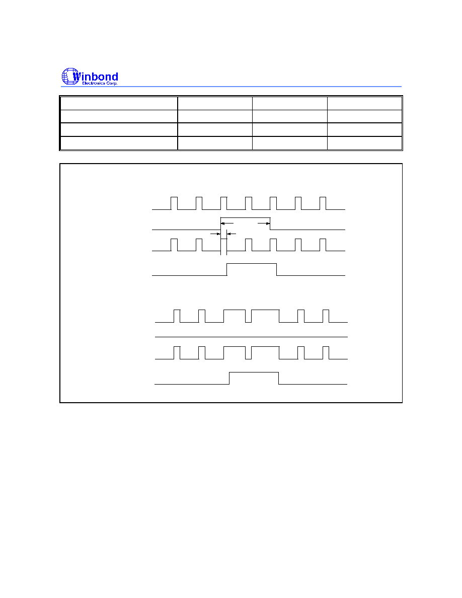
W78C354
- 32 -
F
CLOCK
16 MHz
18.432 MHz
20 MHz
1/Fclock
62.5 nS
54 nS
50 nS
Min. Vsync width (Wvmin)
8031
±
31 nS
6939
±
27 nS
6425
±
25 nS
V
OUT
delay from V
IN
(Tdelay)
8031
±
31 nS
6939
±
27 nS
6425
±
25 nS
H
vmin
1. Withot composite sync
H
V
V
2. With composite sync
delay
T
W
H
IN
V
IN
H
OUT
V
OUT
IN
(H+V)
IN
OUT
OUT
“
Figure 12. Vsync separator output (when DUMMYEN = 0, ENVS = 1)
M-3. Horizontal & Vertical Frequency Counter
There are two 16-bit counters that automatically count the horizontal and vertical frequency. When a
VEVENT interrupt occurs, the W78C354 reads the count value (H
COUNT
and V
COUNT
) from the 8-bit
counter registers (HFCOUNTH, HFCOUNTL, VFCOUNTH, and VFCOUNTL) to calculate the H and V
frequency by the formulas listed below.
W78C354
Publication Release Date: October 1996
- 33 -
Revision A1
V frequency:
∑
Resolution of V frequency counter: V
RESOL
= (1/F
CLOCK
)
◊
16
∑
V-frequency: V
FREQ
= 1/(V
COUNT
◊
V
RESOL
)
∑
Lowest V frequency can be detected: F
CLOCK
°“
1048576
H frequency:
∑
Resolution of H frequency counter: H
RESOL
= (1/F
CLOCK
)
°“
8
∑
H-frequency: H
FREQ
= 1/(H
COUNT
◊
H
RESOL
)
∑
Lowest H frequency can be detected: F
CLOCK
°“
8192
16 MHz
18.432 MHz
20 MHz
Vresol
1
µ
S
868 nS
800 nS
Lowest V
FREQ
15 Hz
17.6 Hz
19 Hz
Hresol
7.8 nS
6.8 nS
6.3 nS
Lowest H
FREQ
1.9 KHz
2.3 KHz
2.4 KHz
M-4. Dummy Frequency Generator
The dummy H and V frequencies are generated for factory burn-in measurement and for displaying a
warning message when there is no input H/V frequency. The dummy sync generator includes two
newly added SFRs, DHREG and DVREG. DHREG is a 4-bit register used to determine the dummy
Hsync output frequency. DVREG is an 8-bit register that can be used to preset a constant into
DVREG to determine the dummy Vsync output frequency by the formulas listed below.
∑
Dummy Hsync frequency F
dH
= F
CLOCK
°“
32
°“
(DHREG+1)
∑
Dummy Vsync frequency F
dV
= F
dH
°“
8
°“
(DVREG+1)
Example: Assume system clock = 16 Mhz
DHREG
F
DH
DVREG
F
DV
15
31.25K
48
79.7 Hz
12
38.5K
59
80.2 Hz
10
45.5K
70
80.1 Hz
9
50K
77
80.1 Hz
7
62.5K
96
80.5 Hz
5
82K
127
80.1 Hz
4
100K
155
80.1 Hz

W78C354
- 34 -
The relations between the bit DUMMYEN and the outputs of the H/V frequencies are listed below:
HOUT
VOUT
DUMMYEN = 0
HREST
VREST (if ENVS = 0)
VSEP (if ENVS = 1)
DUMMYEN = 1
H
DUMMY
V
DUMMY
M-5. H-clamp Pulse Generator
If the P14SF bit is set in the newly added SFR CONTREG4 (bit-addressable), the output pin P1.4 can
be used as the H-clamp pulse output (refer to Figure 13). The Hsync trigger type can be selected to
generate the H-clamp output pulse, and the pulse width of the H-clamp output can be determined by
programming the bits HCES, HCWS1, and HCWS2 in SFR CONTREG1. For details, see the
following figure and description.
CONDITION Of P14SF
PORT 1.4 I/O PIN FUNCTION
P14SF = 0
General I/O pin
P14SF = 1 & P1.4 = 0
H-clamp pulse output
0
1
P14SF
P1.4/HCLAMP
P1.4 output latch
H-Clamp pulse
Figure 13. Alternate function of P1.4
1. Select the leading edge or trailing edge of Hsync:
∑
HCES = 0: select leading edge
∑
HCES = 1: select trailing edge
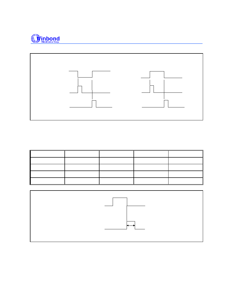
W78C354
Publication Release Date: October 1996
- 35 -
Revision A1
Hsync
Hsync
(a) Negative polarity Hsync
(b) Postive polarity Hsync
(Leading-edge)
(Trailing-edge)
P1.4
P1.4
(Leading-edge)
(Trailing-edge)
P1.4
P1.4
Figure 14. Pin P1.4 outputs the H-clamp pulse at the leading edge or trailing edge of Hsync.
2. Pulse width of H-clamp pulse:
∑
Select the weighting of H-clamp pulse by programming bits HCWS0 and HCWS1 in CONTREG1
∑
Pulse width of H-clamp output: [(1/F
CLOCK
)
◊
Weighting]
±
[ 1/(2
◊
F
CLOCK
)]
(HCWS1, HCWS0)
WEIGHTING
16 MHz
18.432 MHz
20 MHz
(0, 0)
4.5
281
±
31 nS
244
±
27 nS
225
±
25 nS
(0, 1)
8.5
531
±
31 nS
461
±
27 nS
425
±
25 nS
(1, 0)
16.5
1031
±
31 nS
896
±
27 nS
825
±
25 nS
(1, 1)
32.5
2031
±
31 nS
1764
±
27 nS
1625
±
25 nS
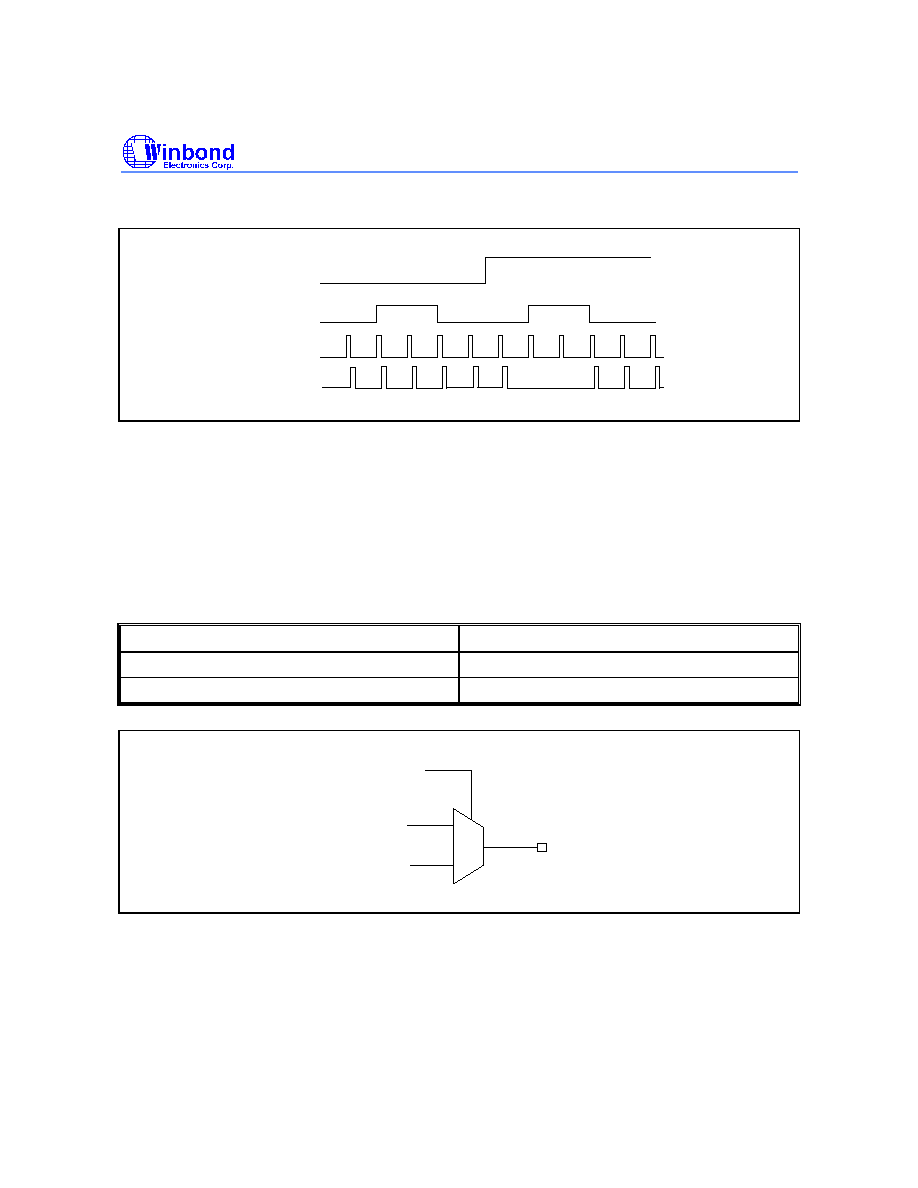
Hsync
H-clamp
output
Figure 15. Pulse width of H-clamp output
W78C354
- 36 -
If the bit VDISHC of SFR CONTREG2 is set high, the H-clamp pulse output will be disabled in the V
sync pulse period.
VDISHC
V
H
H-clamp
IN
IN
Figure 16. Disable H-clamp output
M-6. Safe Operation Area (SOA) Output
The purpose of the SOA output is to protect the HOT (horizontal oscillating transistor) and other
critical circuitry by responding quickly if the Hsync frequency suddenly drops below a preset boundary
frequency. When the Hsync frequency is lower than the preset boundary frequency for three
consecutive cycles or stops for a certain period, the SOA pin (P1.5) will change to a "high" state to
activate an external circuit to protect the monitor. If the bit P15SF is set in SFR CONTREG4, the pin
P1.5 can be used as the SOA output (refer to Figure 17). The SOA pin can be released by writing any
value to SFR SOACLR.
CONDITION Of P15SF
PORT 1.5 I/O PIN FUNCTION
P15SF = 0
General I/O pin
P15SF = 1 & P1.5 = 0
SOA output
0
1
P15SF
P1.5/SOA
P1.5 output latch
SOA output
Figure 17. Alternate function of P1.5
∑
Boundary frequency H
BOUN
D
= 2 MHz
˜
(Value of SOAREG)
Example: If 50 KHz is considered the boundary frequency, then value of SOAREG = 2M
°“
50K =
40.
∑
No Hsync response time = 2048
◊
(1/F
CLOCK
).
W78C354
Publication Release Date: October 1996
- 37 -
Revision A1
16 MHz
18.432 MHz
20 MHz
No Hsync response time
128
µ
S
111
µ
S
102
µ
S
M-7. Self-test Pattern Output
When the dummy frequency generator is enabled, if bit P23SF of SFR CONTREG4 is set, the STP
output will provide a checkerboard pattern for burn-in or self-diagnostic purposes. The bit INVSTP of
CONTREG4 can invert the checkerboard pattern to avoid phosphor damage during factory burn-in.
CONDITION Of P23SF
PORT 2.3 I/O PIN FUNCTION
P23SF = 0
General I/O pin
P23SF = 1 & P2.3 = 0
STP output
0
1
P23SF
P2.3/STP
P2.3 output latch
STP output
Figure 18. Alternate function of P2.3
INVSTP = 0
INVSTP = 1
Figure 19. Checkerboard pattern

W78C354
- 38 -
N. Power Supervisor, Watchdog Timer, and Reset Circuitry
Reset signals can come from three sources: an external reset input (active low), power-low detection,
or the watchdog timer. Figure 20 is a block diagram of the reset circuitry. The power-low detection
circuit generates a reset signal if V
CC
falls below 3.8V, and the reset signal will keep twenty-four
machine cycle after V
CC
rises to 4.3V. Thus we can make sure the chip can be reseted perfectly
when the monitor is first powered on, and avoid the w78c354's overwriting the E
2
PROM mistakenly
when the monitor is powered down. The power-low detection circuit can be enabled or disabled by
code option 1.
The purpose of the watchdog timer is to reset the W78C354 if it enters an abnormal processor state
(caused by electrical noise or RFI, for example). The clock source of the watchdog timer comes from
the internal system clock. The timer can be enabled or disabled by the code option 2. When enabled,
the watchdog circuitry will generate a system reset if the user's program fails to reload the watchdog
timer within a specified length of time after executing the "MOV WDTCLR, # Value" instruction. This
length of time is known as the "watchdog interval" (T
WDT
). Four selections are available for the
watchdog interval (type A, B, C, and D); the selections, which are programmed by code option 3, are
indicated by the formulas in table below.
There are three code options in the reset circuitry:
∑
Code option 1: Enable/disable the power-low detector.
∑
Code option 2: Enable/disable the watchdog timer.
∑
Code option 3: Select one watchdog interval (type A, B, C, D as listed in the table below.)
Watchdog
Timer
Power-low
Detector
Enable/Disable
External reset
System Reset
Code option 2
Code option 1
Enable/Disable
Code option 3
Watchdog interval
Figure 20. Reset circuitry

W78C354
Publication Release Date: October 1996
- 39 -
Revision A1
Table4. Watchdog Interval
T
WDT
F
CLOCK
CODE OPTION 3
FORMULA
16 MHz
18.432 MHz
20 MHz
Type-A
2
19
/F
CLOCK
32 mS
28 mS
26 mS
Type-B
2
21
/F
CLOCK
131 mS
113 mS
104 mS
Type-C
2
23
/F
CLOCK
524 mS
452 mS
417 mS
Type-D
2
24
/F
CLOCK
1048 mS
905 mS
834 mS
ABSOLUTE MAXIMUM RATINGS
PARAMETER
SYMBOL
MIN.
MAX.
UNIT
DC Power Supply
V
CC
-
V
SS
-0.3
+7.0
V
Input Voltage
V
IN
V
SS
-0.3
V
CC
+0.3
V
Operating Temperature
T
A
0
70
∞
C
Storage Temperature
T
ST
-55
+150
∞
C
Note: Exposure to conditions beyond those listed under Absolute Maximum Ratings may adversely affect the life and reliability of the
device.
DC ELECTRICAL CHARACTERISTICS
V
CC
-
V
SS
= 5V
±
10%, T
A
= 25
∞
C, F
OSC
= 20 MHz, unless otherwise specified
PARAMETER
SYM.
CONDITIONS
MIN.
TYP
.
MAX.
UNIT
Operating Voltage
V
DD
4.5
5
5.5
V
Operating Current
I
DD
No load, V
DD
= 5.5V
-
-
65
mA
Idle Current
I
IDLE
Idle mode, V
DD
= 5.5V
-
-
30
mA
Logic 0 Input Current
P1, P2, P3
(except P1.0 to P1.3,P1.5)
I
IN1
V
DD
= 5.5V
V
IN
= 0V
-75
-
-10
µ
A
Input Current
RESET
[*1]
I
IN2
V
DD
= 5.5V
V
IN
= 0V
-250
-
-
µ
A
Input Current
HIN, VIN
[*2]
I
IN3
V
DD
= 5.5V
V
IN
= V
DD
-
-
+30
µ
A
Input Leakage Current
P1.0 to P1.3, ADC0 to
ADC3
I
LK
V
DD
= 5.5V
0V < V
IN
< V
DD
-10
-
+10
µ
A
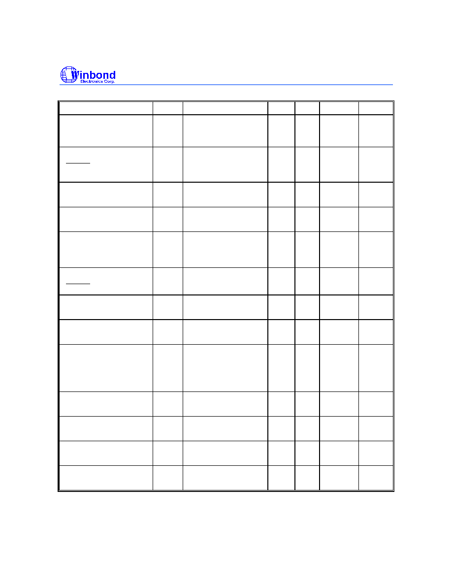
W78C354
- 40 -
DC Electrical Characteristics, continued
PARAMETER
SYM.
CONDITIONS
MIN.
TYP.
MAX.
UNIT
Logical 1-to-0 Transition
Current P1, P2, P3
[*3]
(except P1.0 to P1.3, P1.5)
I
TL
V
DD
= 5.5V
V
IN
= 2.0V
-650
-
-
µ
A
Input Low Voltage
RESET , OSCIN
[*4]
(except P1.0 to P1.3, P1.5)
V
IL1
V
DD
= 4.5V
0
-
0.8
V
Input Low Voltage
HIN, VIN
[*5]
V
IL2
V
DD
= 4.5V
0
-
0.8
V
Input Low Voltage
P1.0 to P1.3
V
IL3
V
DD
= 4.5V
0
-
1.5
V
Input High Voltage
P1, P2, P3
(except P1.0 to P1.3, P1.5)
V
IH1
V
DD
= 5.5V
2.4
-
V
DD
+0.2
V
Input High Voltage
RESET , OSCIN
[*4]
V
IH2
V
DD
= 5.5V
3.5
-
V
DD
+0.2
V
Input High Voltage
HIN, VIN
[*5]
V
IH3
V
DD
= 5.5V
2.4
-
V
DD
+0.2
V
Input High Voltage
P1.0 to P1.3
V
IH4
V
DD
= 5.5V
3.0
-
V
DD
+0.2
V
Output Low Voltage
P1.4, P1.5, P2.2 to P2.7
SDAC0 to SDAC13
H
OUT
, V
OUT
V
OL1
V
DD
= 4.5V
I
OL
= +4 mA
-
-
0.45
V
Output Low Voltage
P1.0, P1.1
V
OL2
V
DD
= 4.5V
I
OL
= +2 mA
-
-
0.4
V
Output Low Voltage
P1.2, P1.3
V
OL3
V
DD
= 4.5V
I
OL
= +6 mA
-
-
0.4
V
Output Low Voltage
P2.0, P2.1
V
OL4
V
DD
= 4.5V
I
OL
= +15 mA
-
-
0.45
V
Output Low Voltage P3,
P4
V
OL5
V
DD
= 4.5V
I
OL
= +2 mA
-
-
0.45
V
W78C354
Publication Release Date: October 1996
- 41 -
Revision A1
DC Electrical Characteristics, continued
PARAMETER
SYM.
CONDITIONS
MIN.
TYP.
MAX.
UNIT
Output Low Voltage
BSDAC0-1, DDAC0-2,
BDDAC
V
OL6
V
DD
= 4.5V
I
OL
= +8 mA
-
-
0.45
V
Output High Voltage
P1.4, P2, P3
V
OH1
V
DD
= 4.5V
I
OH
= -100
µ
A
2.4
-
-
V
Output High Voltage
P1.5, SDAC0-13, H
OUT
,
V
OUT
, Special Function
of P1.4 and P2.3~P2.7
V
OH2
V
DD
= 4.5V
I
OH
= -4 mA
2.4
-
-
V
Output High Voltage,
BSDAC0-1, DDAC0-2,
BDDAC
V
OH3
V
DD
= 4.5V
I
OH
= -8 mA
2.4
-
-
V
Output High Voltage P4
VOH4
V
DD
= 4.5V
I
OH
= -2mA
2.4
-
-
V
Notes:
1. The
RESET
pin has an internal pull-up resistor with a resistance of about 30 K
.
2. Pins HIN and VIN have an internal pull-down resistor with a resistance of about 200 K
.
3. Pins P1, P2, and P3 (except P1.0-P1.3 and P1.5) source a transition current when they are being externally
driven from 1 to 0. The transition current reaches its maximum value when V
IN
is approximately 2V.
4.
RESET
is a Schmitt trigger input, and OSCIN is a CMOS input.
5. HIN and V
IN
are Schmitt trigger inputs.

W78C354
- 42 -
TYPICAL APPLICATION CIRCUIT
H-Size
V-Size
H-Phase
V-Center
SDAC0
SDAC1
SDAC2
SDAC3
SDA
SCL
P2.0
P2.1
HFLB
VFLB
OSD
MC141540
SS
HOUT
VOUT
P2.2
SDAC4
SDAC5
SDAC6
SDAC7
P2.4/SDAC10
P2.5/SDAC11
P2.6/SDAC12
P2.7/SDAC13
Brightness
Contrast
Rotation
R-Gain
B-Gain
R-Cut off
B-Cut off
G-Cut off
CS0
Mute
Degauss
Power saving
TRAP\CBOW\PIN
TILT\BOW
BDDAC
DDAC0
P3.3
P3.4
P3.5
P4.0
VDD
OSCOUT
OSCIN
30P
30P
16M
P4.1
P4.2
P1.4
P1.5
P2.3
CS1
CS2
SOA Output
H-Clamp Output
STP Output
Auto
Alignment
P3.0/RXD
P3.1/TXD
A
D
C
0
/
R
S
T
HIN
VIN
P1.3/DSDA
P1.2/DSCL
24C04
10k
VDD
R1
R2
R3
VDD
S0
S1
S2
R4
10uF
R5
S3
SCL
SDA
R6
R7
P1.1/ISDA
P1.0/ISCL
E PROM
2
VGA
W78C354
R8
VDD
R9

W78C354
Publication Release Date: October 1996
- 43 -
Revision A1
PACKAGE DIMENSIONS
68-pin PLCC
68
61
60
44
43
27
26
10
9
1
L
c
1
b
2
A
H
D
D
e
b
E H
E
y
A
A
1
Seating Plane
D
G
G
E
Notes:
Symbol
Min.
Nom.
Max.
Max.
Nom.
Min.
Dimension In Inches
Dimension In mm
A
b
c
D
e
H
E
L
y
A
A
1
2
E
b
1
H
D
G
G
D
E
on final visual inspection spec.
4. General appearance spec. should be based
3. Controlling dimension: Inches
protrusion/intrusion.
2. Dimension b1 does not include dambar
flash.
1. Dimensions D & E do not include interlead
0.020
0.143
0.026
0.016
0.006
0.949
0.895
0.980
0.090
0.148
0.028
0.018
0.008
0.954
0.915
0.990
0.100
0.050
0.185
0.153
0.032
0.022
0.012
0.959
0.935
1.000
0.110
0.004
0.51
3.63
0.66
0.41
0.15
24.10
22.73
24.90
2.29
3.76
0.71
0.46
0.20
24.23
23.24
25.15
2.54
1.27
4.70
3.89
0.81
0.56
0.30
24.36
23.75
25.40
2.79
0.10
10
0
0
10
0.044
0.056
1.12
1.42
24.36
24.23
24.10
0.959
0.954
0.949
23.75
23.24
22.73
0.935
0.915
0.895
25.40
25.15
24.90
1.000
0.990
0.980
48-pin DIP
Max.
Nom.
Min.
Dimension In Inches
Dimension In mm
A
B
c
D
e
A
L
S
A
A
1
2
E
B
1
1
e
E
1
a
15
E
Seating Plane
Base Plane
B
B
e
1
1
S
D
E
A
L
1
C
A 1
e
A
a
48
1
25
24
A 2
Notes:
1. Dimensions D Max. & S include mold flash or
the bar burrs.
2. Dimension E1 does not include interlead flash.
3. Dimensions D & E1 include mold mismatch and
are determined at the mold parting line.
4. Dimension B1 does not include dambar
protrusion/intrusion.
5. Controlling dimension: Inches.
6. General appearance spec. should be based
on final visual inspection spec.
Min.
Nom.
Max.
Symbol
0
15
0
0.63 0.65 0.67 16.0 16.5 17.0
0.08
2.1
0.12 0.13 0.14
3.0
3.3
3.5
0.55
0.54
0.11
0.55
0.10
0.09
2.2
2.5
2.7
13.8 13.9 14.1
0.60
0.59
0.61 14.9 15.2 15.4
2.45 2.46
62.2 62.4
0.01
0.00
0.01
0.2
0.2
0.3
0.05
0.04
0.05
0.01
0.01
0.02
0.15
0.15
0.16
0.01
0.21
1.2
1.2
1.3
0.4
0.4
0.5
3.8
3.9
4.0
0.2
5.3

W78C354
- 44 -
40-pin DIP
Seating Plane
1. Dimensions D Max. & S include mold flash or
tie bar burrs.
2. Dimension E1 does not include interlead flash.
3. Dimensions D & E1 include mold mismatch and
are determined at the mold parting line.
6. General appearance spec. should be based on
final visual inspection spec.
.
1.372
1.219
0.054
0.048
Notes:
Symbol
Min.
Nom.
Max.
Max.
Nom.
Min.
Dimension In Inches
Dimension in mm
A
B
c
D
e
A
L
S
A
A
1
2
E
0.050
1.27
0.210
5.334
0.010
0.150
0.016
0.155
0.018
0.160
0.022
3.81
0.406
0.254
3.937
0.457
4.064
0.559
0.008
0.120
0.670
0.010
0.130
0.014
0.140
0.203
3.048
0.254
3.302
0.356
3.556
0.540
0.550
0.545
13.72
13.97
13.84
17.01
15.24
14.986
15.494
0.600
0.590
0.610
2.286
2.54
2.794
0.090
0.100
0.110
B
1
1
e
E
1
a
2.055
2.070
52.20
52.58
0
15
0.090
2.286
0.650
0.630
16.00
16.51
protrusion/intrusion.
4. Dimension B1 does not include dambar
5. Controlling dimension: Inches.
15
0
e
A
A
a
c
E
Base Plane
1
A
1
e
L
A
S
1
E
D
1
B
B
40
21
20
1
2
Headquarters
No. 4, Creation Rd. III,
Science-Based Industrial Park,
Hsinchu, Taiwan
TEL: 886-3-5770066
FAX: 886-3-5792697
http://www.winbond.com.tw/
Voice & Fax-on-demand: 886-2-7197006
Taipei Office
11F, No. 115, Sec. 3, Min-Sheng East Rd.,
Taipei, Taiwan
TEL: 886-2-7190505
FAX: 886-2-7197502
Winbond Electronics (H.K.) Ltd.
Rm. 803, World Trade Square, Tower II,
123 Hoi Bun Rd., Kwun Tong,
Kowloon, Hong Kong
TEL: 852-27513100
FAX: 852-27552064
Winbond Electronics North America Corp.
Winbond Memory Lab.
Winbond Microelectronics Corp.
Winbond Systems Lab.
2727 N. First Street, San Jose,
CA 95134, U.S.A.
TEL: 408-9436666
FAX: 408-5441798
Note: All data and specifications are subject to change without notice.