 | –≠–ª–µ–∫—Ç—Ä–æ–Ω–Ω—ã–π –∫–æ–º–ø–æ–Ω–µ–Ω—Ç: W78C378 | –°–∫–∞—á–∞—Ç—å:  PDF PDF  ZIP ZIP |

Preliminary W78E378/W78C378/W78C374
MONITOR CONTROLLER
Publication Release Date: December 1999
- 1 - Revision A1
GENERAL DESCRIPTION
The W78E378, W78C378 and W78C374B are ASIC which is a stand-alone high-performance
microcontroller specially designed for monitor control applications. The device integrates the
embedded 80C31 microcontroller core, on-chip MTP or Mask ROM, 576 bytes of RAM, and a number
of dedicated hardware monitor functions. Additional special function registers are incorporated to
control the on-chip peripheral hardware. The chip is used to control the interface signal of other
devices in the monitor and to process the video sync signals. Because of the highly integration and
Flash cell for program memory, the device can offer users the competitive advantages of low cost
and reduced development time.
FEATURES
∑
80C31 MCU Core Embedded
∑
32K Bytes MTP-ROM (W78E378)
∑
32K Bytes Mask-ROM (W78C378)
∑
16K Bytes Mask-ROM (W78C374B)
∑
Total 576 Bytes of On-chip Data RAM
-
256 bytes accessed as in the 80C32
-
320 bytes accessed as external data memory via "MOVX @Ri"
∑
PWM DACs
-
Eight 8-bit Static PWM DACs: DAC0
-
DAC8
-
Three 8-bit Dynamic PWM DACs: DAC9
-
DAC10
∑
Sync Processor
-
Horizontal & Vertical Polarity Detector
-
Sync Separator for Composite Sync
-
12-bit Horizontal & Vertical Frequency Counter
-
Programmable Dummy Frequency Generator
-
Programmable H-clamp Pulse Output
-
SOA Interrupt
-
Hsync/2 Output
∑
Serial Ports:
-
DDC1 Port- support DDC1
-
SIO1 & SIO2 Ports - each can support DDC2B/2B+/2Bi/2AB (each has 2 slave addresses)
∑
Two 16-bit Timer/Counters (8031's Timer0 & Timer1)
∑
One External Interrupt Input (8031's INT0 )
∑
One Parabola Interrupt Generator
∑
One ADC with 7 Multiplexed Analog Inputs
∑
Two 12 mA(min) Output Pins for Driving LEDs
∑
Watchdog Timer (2
22
/Fosc = 0.42s @Fosc = 10 MHz)
∑
Power Low Reset
∑
Frequency: 10 MHz max. (with the same performance as a normal 8051 that uses 20 MHz)
∑
Packaged in 40/32-pin 600 mil DIP & 44-pin PLCC

Preliminary W78E378/W78C378/W78C374
- 2 -
PIN CONFIGURATIONS
40-pin DIP:
W78E378E
40-pin DIP
W78C378E
P4.1
1
40
P4.2
W78C374E
P4.0 (HFI)
2
32-pin DIP
39
P4.3
P3.5 (ADC4, T0)*
3
1
32
38
P3.6 (ADC5, T1)*
P1.1 (DAC1)*
4
2
31
37
P1.2 (DAC2)*
32-pin DIP:
W78E378
P1.0 (DAC0)*
5
3
30
36
P1.3 (DAC3)*
W78C378
P3.4 (VOUT)
6
4
29
35
P1.4 (DAC4)*
W78C374
P3.3 (HOUT)
7
5
28
34
P1.5 (DAC5)*
H
IN
8
6
27
33
P1.6 (DAC6)*
V
IN
9
7
26
32
P1.7 (DAC7)*
RESET
10
8
25
31
P2.0 (DAC8)
V
DD
11
9
24
30
P2.1 (DAC9)
V
SSA
12
10
23
29
P2.2 (DAC10)
OSCOUT
13
11
22
28
P2.3 (Hclamp)
OSCIN
14
12
21
27
P2.4 (ADC0)
P3.2 ( INT0 )
15
13
20
26
P2.5 (ADC1)
P3.1 (SCL)*
16
14
19
25
P2.6 (ADC2)
P3.0 (SDA)*
17
15
18
24
P2.7 (ADC3)
V
SS
18
16
17
23
P3.7 (ADC6)*
P4.7 (HFO)
19
22
P4.4 (SCL2)*
P4.6
20
21
P4.5 (SDA2)*
44-pin PLCC
H
V
RESET
V
V
VDDA
VSSA
OSCOUT
OSCIN
NC
P1.5
P1.6
P1.7
P2.0
P2.1
P2.2
P2.3
P
3
.
1
V
S
S
P
3
.
0
P
3
.
7
P
4
.
6
P
4
.
5
P
4
.
4
P
4
.
7
7
8
9
10
11
12
13
14
15
16
17
1
8
1
9
2
0
2
2
2
6
2
5
2
4
2
3
2
8
2
1
2
7
39
29
30
32
33
31
35
34
36
37
38
1
2
3
4
5
6
4
0
4
1
4
2
4
3
4
4
P
3
.
4
P
1
.
0
P
1
.
1
P
3
.
5
P
3
.
6
P
1
.
2
P
4
.
3
P
1
.
3
P3.2
P3.3
P
4
.
2
P
4
.
1
P
4
.
0
P1.4
P2.5
P2.4
P
2
.
7
P
2
.
6
V
S
S
W78E378P
W78C378P
W78C374P
DD
DD
IN
IN

Preliminary W78E378/W78C378/W78C374
Publication Release Date: December 1999
- 3 - Revision A1
PIN DESCRIPTION
PIN NAME
I/O
DESCRIPTION
RESET
I/O Chip reset input (active low) input &
Internal reset output (generated by WDT or power low)
TTL Schmitt trigger input, internal pull-up ~30 K
I
OL
= +12 mA @V
OL
= 0.45V
V
DD
-
Positive power supply
V
SS
-
Ground
V
SS
-
Ground
OSC
OUT
O Output from the inverting oscillator amplifier
OSC
IN
I
Input to the inverting oscillator amplifier, 10 MHz max.
H
IN
I
Hsync input
TTL Schmitt trigger input , w/o PMOS
V
IH
/V
IL
= 2.0V/0.8V, V+/ V- = ~1.6V/ 1.1V
V
IN
I
Vsync input
TTL Schmitt trigger input, w/o PMOS
V
IH
/V
IL
= 2.0V/0.8V, V+/ V- = ~1.6V/ 1.1V
P1.0 (DAC0)
I/O General purpose I/O, DAC0 special function output
Open-drain output, sink current: 15 mA
P1.1 (DAC1)
I/O General purpose I/O, DAC1 special function output
Open-drain output, sink current: 15 mA
P1.2 (DAC2)
I/O General purpose I/O, DAC2 special function output
Open-drain output, sink current: 4 mA
P1.3 (DAC3)
I/O General purpose I/O, DAC3 special function output
Open-drain output, sink current: 4 mA
P1.4 (DAC4)
I/O General purpose I/O, DAC4 special function output
Open-drain output, sink current: 4 mA
P1.5 (DAC5)
I/O General purpose I/O, DAC5 special function output
Open-drain output, sink current: 4 mA
P1.6 (DAC6)
I/O General purpose I/O, DAC6 special function output
Open-drain output, sink current: 4 mA
P1.7 (DAC7)
I/O General purpose I/O, DAC7 special function output
Open-drain output, sink current: 4 mA

Preliminary W78E378/W78C378/W78C374
- 4 -
Pin Description, Continued
PIN NAME
I/O
DESCRIPTION
P2.0 (DAC8)
I/O General purpose I/O, DAC8 Special Function output
Sink/Source current: 4 mA/-100
µ
A (-4 mA for SF output)
P2.1 (DAC9)
I/O General purpose I/O, DAC9 Special Function output
Sink/Source current: 4 mA/-100
µ
A (-4 mA for SF output)
P2.2 (DAC10)
I/O General purpose I/O, DAC10 Special Function output
Sink/Source current: 4 mA/-100
µ
A (-4 mA for SF output)
P2.3 (Hclamp)
I/O General purpose I/O, Hclamp Special Function output
Sink/Source current: 4 mA/-100
µ
A (-4 mA for SF output)
P2.4 (ADC0)
I/O General purpose I/O, ADC input channel 0
Sink/Source current: 4 mA/-100
µ
A
P2.5 (ADC1)
I/O General purpose I/O, ADC input channel 1
Sink/Source current: 4 mA/-100
µ
A
P2.6 (ADC2)
I/O General purpose I/O, ADC input channel 2
Sink/Source current: 4 mA/-100
µ
A
P2.7 (ADC3)
I/O General purpose I/O, ADC input channel 3
Sink/Source current: 4 mA/-100
µ
A
P3.0 (SDA)
I/O General purpose I/O, DDC port serial data I/O
Schmitt trigger input
V
IH
/V
IL
= 0.7 V
DD
/0.3 V
DD
, V+/V- = ~0.6 V
DD
/ 0.4 V
DD
Open-drain output, sink current: 8 mA
P3.1 (SCL)
I/O General purpose I/O, DDC port serial clock I/O
Schmitt trigger input
V
IH
/V
IL
= 0.7 V
DD
/0.3 V
DD
, V+/V- = ~0.6 V
DD
/ 0.4 V
DD
Open-drain output, sink current: 8 mA
P3.2 ( INT0 )
I/O General purpose I/O, INT0 input
Sink/Source current: 1 mA/ -100
µ
A
P3.3 (H
OUT
)
I/O General purpose I/O, H
OUT
special function output
Sink/Source current: 4 mA/-100
µ
A (-4 mA for SF output)
P3.4 (V
OUT
)
I/O General purpose I/O, V
OUT
special function output
Sink/Source current: 4 mA/-100
µ
A (-4 mA for SF output)
P3.5 (ADC4, T0) I/O General purpose I/O, ADC input channel 4
Open-drain output, sink current: 4 mA
P3.6 (ADC5, T1) I/O General purpose I/O, ADC input channel 5
Open-drain output, sink current: 4 mA
P3.7 (ADC6)
I/O General purpose I/O, ADC input channel 6
Open-drain output, sink current: 4 mA
Preliminary W78E378/W78C378/W78C374
Publication Release Date: December 1999
- 5 - Revision A1
Pin Description, Continued
PIN NAME
I/O
DESCRIPTION
P4.0 (HFI)
I/O P4.0 Output, HFI Input
Sink/Source current: 4 mA/-4 mA
P4.1
O
P4.1 Output
Sink/Source current: 4 mA/-4 mA
P4.2
O
P4.2 Output
Sink/Source current: 4 mA/-4 mA
P4.3
O
P4.3 Output
Sink/Source current: 4 mA/-4 mA
P4.4 (SCL2)
I/O P4.4 Output, SIO2 port serial clock I/O
Schmitt trigger input
V
IH
/V
IL
= 0.7 V
DD
/0.3 V
DD
, V+/V- = ~0.6 V
DD
/0.4 V
DD
Open-drain output, sink current: 8 mA
P4.5 (SDA2)
I/O P4.5 Output, SIO2 port serial data I/O
Schmitt trigger input
V
IH
/V
IL
= 0.7 V
DD
/0.3 V
DD
, V+/V- = ~0.6 V
DD
/0.4 V
DD
Open-drain output, sink current: 8 mA
P4.6
O
P4.6 Output
Sink/Source current: 4 mA/-4 mA
P4.7 (HFO)
O
P4.7 Output, HFO Output
Sink/Source current: 4 mA/-4 mA
Preliminary W78E378/W78C378/W78C374
- 6 -
BLOCK DIAGRAM
CPU
Osc.
Circuit
Reset
Circuit
Power Low
Detection
INT0 (P3.2)
Interrupt
Processor
Timer 0
Timer 1
OSCIN
OSCOUT
80C31 Core excluding internal RAM
ADC
ADC0 (P2.4)
ADC1 (P2.5)
ADC2 (P2.6)
ADC3 (P2.7)
ADC4 (P3.5)
ADC5 (P3.6)
ADC6 (P3.7)
VPP (P3.2)
V
V
8-bit Internal Bus
Watch Dog
Timer
Sync.
Processor
P4
I/O Port
Static DACs
Dynamic DACs
DAC0~7 (P1.0~P1.7)
DAC8~10 (P2.0~P2.2)
SIO1
SCL (P3.1)
SDA (P3.0)
RESET
Program Memory
RAM: 576 Bytes
Data Memory
T0 (P3.5)
T1 (P3.6)
Note:
P1, P4.4~P4.5
P3.0~P3.1 & P3.5~P3.7
are open-drain.
Note:
freq1 = freq2
freq1
freq2
P1, P2, P3
SIO2
SCL2 (P4.4)
SDA2 (P4.5)
HIN, VIN
HFI (P4.0)
VOUT (P3.4)
HOUT (P3.3)
Hclamp (P2.3)
HFO (P4.7)
DD
SS
Preliminary W78E378/W78C378/W78C374
Publication Release Date: December 1999
- 7 - Revision A1
FUNCTIONAL DESCRIPTION
Address Space
Direct Addressing
"MOV"
Indirect Addressing
"MOV @Ri"
Internal RAM
256 Bytes
8051SFRs &
Serial Ports SFRs
Internal
Program Memory
External Access
"MOVX @Ri"
On-Chip Data Memory
128 Bytes
00h
80h
FFh
00h
Direct or Indirect
Addressing
"MOV" or "MOV @Ri"
new SFRs
80h
External Access
"MOVX @Ri"
0000h
External Access
"MOVX @Ri"
On-Chip Data Memory
64 Bytes
C0h
On-Chip Data Memory
128 Bytes
00h
External Access
"MOVX @Ri"
BANK0
BANK1
FFh
7Fh
7Fh
7Fh
BFh
7FFFh
External Access
"MOVX @Ri"
(3FFFh)
Program/Data/SFRs Address Space
SFRs accessed using 'Direct Addressing'
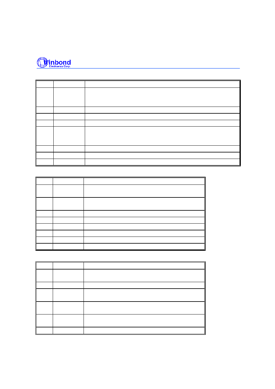
REGISTER
ADDRESS
BITS
POWER
ON RESET
RESET
R/W
1
A*
E0h
8
00h
00h
R/W
2
B*
F0h
8
00h
00h
R/W
3
PSW*
D0h
8
00h
00h
R/W
4
SP
81h
8
00h
00h
R/W
5
DPL
82h
8
00h
00h
R/W
6
DPH
83h
8
00h
00h
R/W
7
IE*
A8h
8
00h
00h
R/W
8
IP*
B8h
8
00h
00h
R/W
9
TCON*
88h
8
00h
00h
R/W
10
TMOD
89h
8
00h
00h
R/W
11
TL0
8Ah
8
00h
00h
R/W
12
TH0
8Ch
8
00h
00h
R/W
13
TL1
8Bh
8
00h
00h
R/W
14
TH1
8Dh
8
00h
00h
R/W
15
PCON
87h
8
00h
x0h
R/W

Preliminary W78E378/W78C378/W78C374
- 8 -
SFRs accessed using 'Direct Addressing', continued
REGISTER
ADDRESS
BITS
POWER
ON RESET
RESET
R/W
16
P1*
90h
8
00h
00h
R/W
17
P2*
A0h
8
FFh
FFh
R/W
18
P3*
B0h
8
1Fh
1Fh
R/W
19
TMREG*
C0h
3
00h
xxh
R/W
20
S1CON*
D8h
8
00h
00h
R/W
21
S1STA
D9h
8
F8h
F8h
R
22
S1DAT
DAh
8
FFh
FFh
R/W
23
S1ADR1
DBh
8
00h
00h
R/W
24
S1ADR2
DCh
8
00h
00h
R/W
25
S2CON*
E8h
8
00h
00h
R/W
26
S2STA
E9h
8
F8h
F8h
R
27
S2DAT
EAh
8
FFh
FFh
R/W
28
S2ADR1
EBh
8
00h
00h
R/W
28
S2ADR2
ECh
8
00h
00h
R/W
Notes:
1. The SFRs marked with an asterisk (*) are both bit- and byte-addressable.
2. Port 1 and P3.5
-
P3.7 outputs low during & after reset.
3. "x" means no reset action.
4. The SFRs in the shaded region are new-defined.
* Modified
PCON
BIT
NAME
FUNCTION
0
ADCS2
ADC channel Select bit 2
1
PD
Power Down bit
2
GF0
General purpose flag bit
3
GF1
General purpose flag bit
4
TEST0
Test purpose flag bit
5
TEST1
Test purpose flag bit
6
ADCcal
Set 0/1 to select 1.0V/3.0V for ADC calibration
7
CPUhalt
Set to let CPU halt when the chip runs internally
*
TMREG: Test Mode Register
BIT
NAME
FUNCTION
0
TM1
Test Mode1
1
TM2
Test Mode2
2
TM3
Test Mode3
Preliminary W78E378/W78C378/W78C374
Publication Release Date: December 1999
- 9 - Revision A1
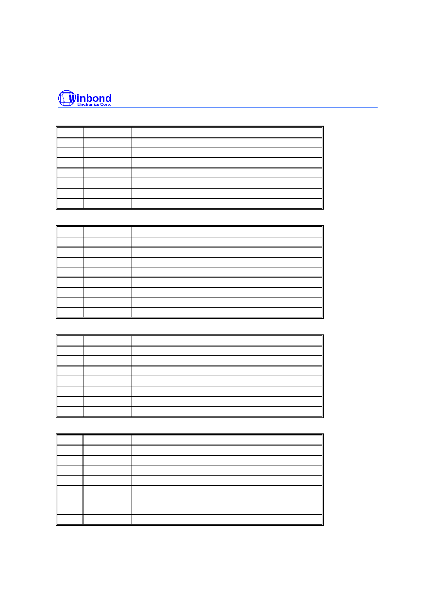
SFRs accessed using 'MOVX @Ri'
REGISTER
ADDRESS
BITS
POWER
ON RESET
RESET
R/W
TYPE
1
CTRL1
80h
8
00h
00h
W
2
CTRL2
81h
8
00h
00h
W
3
P1SF
82h
8
00h
xxh
W
4
P2SF
83h
8
00h
xxh
W
5
P3SF
84h
8
00h
00h
W
6
PARAL
85h
8
00h
00h
R/W
7
PARAH
86h
5
00h
00h
R/W
8
HFCOUNTL
87h
8
x
x
R
9
HFCOUNTH
88h
8
x
x
R
10
VFCOUNTL
89h
8
x
x
R
11
VFCOUNTH
8Ah
8
x
x
R
12
WDTCLR
8Bh
-
x
x
W
13
SOARL
8Ch
8/6
x
x
R/W
14
SOARH
8Dh
8/6
x
x
R/W
15
SOACLR
8Eh
-
x
x
W
16
INTMSK
8Fh
6
00h
00h
R/W
17
INTVECT
90h
6
00h
00h
R
18
INTCLR
91h
6
x
x
W
19
DDC1
92h
8
x
x
W
20
ADC
93h
8
x
x
R
21
DAC0
94h
8
00h
x
R/W
22
DAC1
95h
8
00h
x
R/W
23
DAC2
96h
8
00h
x
R/W
24
DAC3
97h
8
00h
x
R/W
25
DAC4
98h
8
00h
x
R/W
26
DAC5
99h
8
00h
x
R/W
27
DAC6
9Ah
8
00h
x
R/W
28
DAC7
9Bh
8
00h
x
R/W
29
DAC8
9Ch
8
00h
x
R/W
30
DAC9
9Dh
8
00h
x
R/W
31
DAC10
9Eh
8
00h
x
R/W
32
P4
9Fh
8
FFh
FFh
W
33
CTRL3
A0h
0
00h
00h
W
Note: "x" means no reset action.
Preliminary W78E378/W78C378/W78C374
- 10 -
*
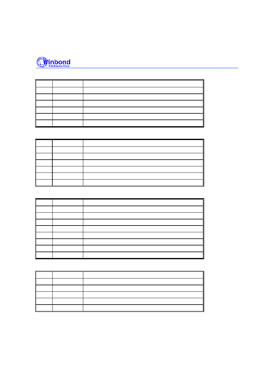
CTRL1: Control Register 1 (Write Only)
BIT
NAME
FUNCTION
0
ADCSTRT
A-to-D Conversion START control
Set by S/W to start conversion.
Cleared by H/W while conversion completed (read SOARH.6 to check).
1
ADCS0
ADC channel Select bit 0
2
ADCS1
ADC channel Select bit 1
3
ENDDC1
Enable DDC1
4
HCES
H-Clamp Edge Select
0: Select leading edge of restored Hsync
1: Select trailing edge of restored Hsync
5
HCWS
H-Clamp Width Select bit
6
DUMMYEN
Dummy signal Enable
7
VSDIS
Vsync Separator Disable, 0: Enable, 1: Disable
*
CTRL2: Control Register 2 (Write Only)
BIT
NAME
FUNCTION
0
HSPS
HSync Polarity Select
0: Positive, 1: Negative
1
VSPS
VSync Polarity Select
0: Positive, 1: Negative
2
HDUMS0
H Dummy frequency Select 0
3
VDUMS
V Dummy frequency Select
4
DDC1B9
Bit 9 in DDC1 mode
5
WDTEN
Enable Watch Dog Timer
6
SOAHDIS
Disable SOA low to high detection
7
OSCHI
OSC freq. Higher than 10 MHz
*
CTRL3: Control Register 3 (Write Only)
BIT
NAME
FUNCTION
0
ENHFO
Enable HF input/output for P4.0/P4.7, respectively
0: Disable, 1: Enable
1
HDUMS1
H Dummy frequency Select 1
2
HFO_POL
Select HFO polarity
0: Positive, 1: Negative
3
HFO_HALF
Select HFO output freq.
0: the same as HFI, 1: half of the HFI
4
ENBNK1
Select on-chip ext. RAM bank
0: Bank 0, 1: Bank 1
5
-
7
-
-
Preliminary W78E378/W78C378/W78C374
Publication Release Date: December 1999
- 11 - Revision A1
*P1SF: Port1 special function output enable register (Write Only)
BIT
NAME
FUNCTION
0
P10SF
Port 1.0 Special Function enable (DAC0 output)
1
P11SF
Port 1.1 Special Function enable (DAC1 output)
2
P12SF
Port 1.2 Special Function enable (DAC2 output)
3
P13SF
Port 1.3 Special Function enable (DAC3 output)
4
P14SF
Port 1.4 Special Function enable (DAC4 output)
5
P15SF
Port 1.5 Special Function enable (DAC5 output)
6
P16SF
Port 1.6 Special Function enable (DAC6 output)
7
P17SF
Port 1.7 Special Function enable (DAC7 output)
*P2SF: Port2 special function output enable register (Write Only)
BIT
NAME
FUNCTION
0
P20SF
Port 2.0 Special Function enable (DAC8 output)
1
P21SF
Port 2.1 Special Function enable (DAC9 output)
2
P22SF
Port 2.2 Special Function enable (DAC10 output)
3
P23SF
Port 2.3 Special Function enable (Hclamp output)
4
P24SF
Port 2.4 Special Function enable (ADC0 input)
5
P25SF
Port 2.5 Special Function enable (ADC1 input)
6
P26SF
Port 2.6 Special Function enable (ADC2 input)
7
P27SF
Port 2.7 Special Function enable (ADC3 input)
*P3SF: Port3 special function output enable register (Write Only)
BIT
NAME
FUNCTION
0
-
2
-
-
3
P33SF
Port 3.3 Special Function enable (H
OUT
)
4
P34SF
Port 3.4 Special Function enable (V
OUT
)
5
-
7
-
-
*HFCOUNTL: Horizontal frequency counter register, low byte (Read Only)
BIT
NAME
FUNCTION
0
HF0
H frequency count bit 0
1
HF1
H frequency count bit 1
2
HF2
H frequency count bit 2
3
HF3
H frequency count bit 3
4
HF4
H frequency count bit 4
5
HF5
H frequency count bit 5
6
HF6
H frequency count bit 6
7
HF7
H frequency count bit 7
Preliminary W78E378/W78C378/W78C374
- 12 -
*HFCOUNTH: Horizontal frequency counter register, high byte (Read Only)
BIT
NAME
FUNCTION
0
HF8
H frequency count bit 8
1
HF9
H frequency count bit 9
2
HF10
H frequency count bit 10
3
HF11
H frequency count bit 11
4
-
5
-
-
6
NOH
Set by hardware if no Hin signal
7
HPOL
Hin polarity. 0: Positive, 1: Negative
*VFCOUNTL: Vertical frequency counter register, low byte (Read Only)
BIT
NAME
FUNCTION
0
VF0
V frequency count bit 0
1
VF1
V frequency count bit 1
2
VF2
V frequency count bit 2
3
VF3
V frequency count bit 3
4
VF4
V frequency count bit 4
5
VF5
V frequency count bit 5
6
VF6
V frequency count bit 6
7
VF7
V frequency count bit 7
*VFCOUNTH: Vertical frequency counter register, high byte (Read Only)
BIT
NAME
FUNCTION
0
VF8
V frequency count bit 8
1
VF9
V frequency count bit 9
2
VF10
V frequency count bit 10
3
VF11
V frequency count bit 11
4
-
5
-
-
6
NOV
Set by hardware if no V
IN
signal
7
VPOL
V
IN
polarity. 0: Positive, 1: Negative
*
INTVECT: Interrupt Vector Register (Read Only)
BIT
NAME
FUNCTION
0
SCLINT
SCL pin pulled low detected
1
ADCINT
ADC conversion completed
2
DDC1INT
DDC1 port buffer empty
3
SOAINT
SOA condition happen
4
VEVENT
Vsync pulse detected or NOV = 1 (V counter overflow)
(The VEVENT is designed to be generated only 'one' time
if no Vsync input.)
5
PARAINT
Parabola Interrupt generated
Preliminary W78E378/W78C378/W78C374
Publication Release Date: December 1999
- 13 - Revision A1
*
INTMSK: Interrupt Mask Register (Read/Write)
BIT
NAME
FUNCTION
0
MSCLINT
Set/clear to enable/disable SCLINT
1
MADCINT
Set/clear to enable/disable ADCINT
2
MDDC1INT Set/clear to enable/disable DDC1INT
3
MSOAINT
Set/clear to enable/disable SOAINT
4
MVEVENT Set/clear to enable/disable VEVENT
5
MPARAINT Set/clear to enable/disable PARAINT
*
INTCLR (Write Only)
BIT
NAME
FUNCTION
0
CSCLINT
Write 1 to this bit to clear SCLINT in INTVECT
1
CADCINT
Write 1 to this bit to clear ADCINT in INTVECT
2
CDDC1INT Write 1 to this bit to clear DDC1INT in INTVECT
3
CSOAINT
Write 1 to this bit to clear SOAINT in INTVECT
4
CVEVENT
Write 1 to this bit to clear VEVENT in INTVECT
5
CPARAINT Write 1 to this bit to clear PARAINT in INTVECT
*PARAL: Parabola interrupt generator register, low byte (Read/Write)
BIT
NAME
FUNCTION
0
PARA0
PARAINT period register bit 0
1
PARA1
PARAINT period register bit 1
2
PARA2
PARAINT period register bit 2
3
PARA3
PARAINT period register bit 3
4
PARA4
PARAINT period register bit 4
5
PARA5
PARAINT period register bit 5
6
PARA6
PARAINT period register bit 6
7
PARA7
PARAINT period register bit 7
*PARAH: Parabola interrupt generator register, high byte (Read/Write)
BIT
NAME
FUNCTION
0
PARA8
PARAINT period register bit 8
1
PARA9
PARAINT period register bit 9
2
PARA10
PARAINT period register bit 10
3
PARA11
PARAINT period register bit 11
4
PARA12
PARAINT period register bit 12
Preliminary W78E378/W78C378/W78C374
- 14 -
*SOARL: SOA register, low byte (Read/Write)
BIT
NAME
FUNCTION
0
SL0
SOA Low register bit 0
1
SL1
SOA Low register bit 1
2
SL2
SOA Low register bit 2
3
SL3
SOA Low register bit 3
4
SL4
SOA Low register bit 4
5
SL5
SOA Low register bit 5
6
(OVL)
OVL = 1: current H count larger than SOARL, for test
7
(OVH)
OVH = 1: current H count smaller than SOARH, for test
*SOARH: SOA register, high byte (Read/Write)
BIT
NAME
FUNCTION
0
SH0
SOA High register bit 0
1
SH1
SOA High register bit 1
2
SH2
SOA High register bit 2
3
SH3
SOA High register bit 3
4
SH4
SOA High register bit 4
5
SH5
SOA High register bit 5
6
(ADCSTRT) ADCSTRT bit status, for test
7
(WDTQ10) Watch Dog Timer, bit 10, for test
*
ADC
Result of the A-to-D conversion.
* DAC0~DAC8
8-bit PWM static DAC register.
*
DAC9~DAC10
8-bit PWM dynamic DAC register.
*
WDTCLR
Watchdog-timer-clear register, without real hardware but an address.
Writing any value to WDTCLR will clear the watchdog timer.
*
SOACLR
Safe-Operation-Area Clear register, without real hardware but an address.
Writing any value to SOACLR will clear the SOAINT.
* DDC1
DDC1 latch buffer.
*
S1CON
SIO1 control register.
*
S1STA
SIO1 status register.
*
S1DAT
SIO1 data register.
*
S1ADR1, S1ADR2 SIO1 address registers.
*
S2CON
SIO2 control register.
*
S2STA
SIO2 status register.
*
S2DAT
SIO2 data register.
*
S2ADR1, S2ADR2 SIO2 address registers.
Preliminary W78E378/W78C378/W78C374
Publication Release Date: December 1999
- 15 - Revision A1
Modified Timer 0 & Timer 1
OSC
6
.
.
TR0
GATE
INT0 pin
(P3.2)
T0 pin
(P3.5)
C/T = 0
C/T = 1
Modified point in Timer 0
(Not divided by 12)
To TL0
OSC
6
.
.
TR1
GATE
T1 pin
(P3.6)
C/T = 0
C/T = 1
Modified point in Timer 1
(Not divided by 12)
To TL1
V
Modified point in Timer 1
(No INT1 pin)
DD
Preliminary W78E378/W78C378/W78C374
- 16 -
DDC1/SIO1 and SIO2 Ports
1. DDC1/SIO1 port
DDC1
ENDDC1
DDC Port
SCL
SDA
SIO1
Support DDC2B/2B+
Support DDC1
IN
IN
OUT
OUT
OUT
SCL
SDA
SDA
SCL
0
1
Vsync
∑
ENDDC1 = 1, used as DDC1 (Display Data Channel) port:
To support DDC1, use Vsync signal for shift clock and P3.0 (SDA) for data output.
∑
ENDDC1 = 0, used as SIO1 port:
To support DDC2B/2B+/2Bi/2AB, use P3.1 (SCL) for serial clock and P3.0 (SDA) for serial data.
SCLINT interrupt is generated when SCL (P3.1) has a high-to-low transition and then keeps at low for
16
◊
1/Fosc.
Fosc
8 MHz
10 MHz
SCL low
2
µ
S
1.6
µ
S
2. SIO2 port:
∑
To support DDC2B/2B+/2Bi/2AB, use P4.4 (SCL) for serial clock and P4.5 (SDA) for serial data.
DDC1 Port
The DDC1 is a serial output port that supports DDC1 communication. To enable the DDC1 port,
ENDDC1 (bit 3 of CTRL1) should be set to '1'. Once previous eight data bits in the shift register and
one null bit (the 9th bit) are shifted out to the SDA sequentially on each
rising edge of the V
IN
signal,
the DDC1 control circuit loads the next data byte from the latch buffer (the DDC1 register) to the shift
register and generates a DDC1INT signal to the CPU. In the interrupt service routine, the S/W should
fetch the next byte of EDID data and write it to the DDC1 register. If ENDDC1 is cleared, the shift
register is stopped, and the SDA output is kept high. The bit DDC1B9 (bit 4 of CTRL2) decides the 9th
bit in a DDC transmission. If DDC1B9 is set, the 9th bit will be '1', otherwise '0'.

Preliminary W78E378/W78C378/W78C374
Publication Release Date: December 1999
- 17 - Revision A1
To use DDC1 port, a user should pay attention to the following items:
(1) When the chip is powered-on or after reset , the 8-bit shift register in DDC1 H/W contains all 0s. If
you write a data to the latch buffer (the DDC1 register), it will be loaded to the shift register at the
9th clock (on V
IN
), so from the 10th clock, the real data bit begins to shift out.
(2) Because there is no reset signal to the latch buffer, it contains a random data after power-on. If
you enable DDC1 without writing data to the latch buffer, SDA will have the random data shifted
out after 9 clocks. The shift register is reset to 00H during CPU reset.
(3) The DDC1 H/W has a counter that counts how many bits shifted out. This counter is initialized to 0
when power-up or reset. When you firstly enable DDC1 after power-on, the first bit is already
shifted out without clock, so the first clock triggers the second data bit (D6) to shift out and "0000
0001 1" will be got. After the first 9 clocks that shift out an invalid byte, the counter counts from 1
to 9 cyclically according to the clock pulse on V
IN
-pin. See the following illustration.
After power on, the
counter count:
0 1 2 3 4 5 6 7 8 9 1 2 3 4 5 6 7 8 9 1 2 3 4 5 6 7 8 9 ...
shifted-out data bit:
0
0 0 0 0 0 0 0 1
1
D7 D6 D5 D4 D3 D2 D1 D0
ack
D7 D6 D5 D4 D3 D2 D1 D0
ack ...
V
IN
clock pulse:
1 2 3 4 5 6 7 8 9 1 2 3 4 5 6 7 8 9 1 2 3 4 5 6 7 8 9 ...
|--> invalid data |--> normal data
(4) The interrupt happens on the failing edge of the following first clock. The next data, which is about
to be shifted out, in the latch buffer is loaded into the shift register at the rising edge of the
following first clock. At the same time, data bit D7 is shifted out and the counter value is "1".
SIO1 Port (with two slave addresses)
The SIO1 port is a serial I/O port, which supports all transfer modes from and to the I
2
C bus. The
SIO1 port handles byte transfers autonomously. To enable this port, the bit ENDDC1 in CTRL1
should be cleared to '0'. The CPU interfaces to the SIO1 port through the following five special
function registers:
S1CON (control register, D8h), S1STA (status register, D9h), S1DAT (data
register, DAh) and
S1ADR1/S1ADR2 (address registers, DBh/DCh). The SIO1 H/W interfaces to the
I
2
C bus via two pins: SDA (P3.0, serial clock line) and SCL (P3.1, serial data line). The output latches
of P3.0 and P3.1 must be set to "1" before using this port.
SIO2 Port (with two slave addresses)
The function of this port is the same as SIO1 port. The CPU interfaces to the SIO2 port through the
following five special function registers:
S2CON (control register, E8h), S2STA (status register, E9h),
S2DAT (data register, EAh) and S2ADR1/S2ADR2 (address registers, EBh/ECh). The SIO2 H/W
interfaces to the I
2
C bus via two pins: SDA2 (P4.5, serial clock line) and SCL2 (P4.4, serial data line).
The output latches of P4.5 and P4.4 must be set to "1" before using this port.
Operation of SIO1 Port: (SIO2 has the same function except their addresses of control registers)
Preliminary W78E378/W78C378/W78C374
- 18 -
a) Control Registers
a-1) The Address Registers, S1ADR1, S1ADR2
The SIO1 is equipped with two address registers: S1ADR1 & S1ADR2. The CPU can read from and
write to these two 8-bit, directly addressable SFRs. The content of these registers are irrelevant when
SIO1 is in master modes. In the slave modes, the seven most significant bits must be loaded with the
MCU's own address. The SIO1 hardware will react if either of the addresses is matched.
7
6
5
4
3
2
1
0
X
X
X
X
X
X
X
-
|------------------------ Own Slave Address -----------------------|
a-2) The Data Register, S1DAT
This register contains a byte of serial data to be transmitted or a byte which has just been received.
The CPU can read from or write to this 8-bit directly addressable SFR while it is not in the process of
shifting a byte. This occurs when SIO1 is in a defined state and the serial interrupt flag (SI) is set.
Data in S1DAT remains stable as long as SI is set. While data is being shifted out, data on the bus is
simultaneously being shifted in; S1DAT always contains the last data byte present on the bus. Thus,
in the event of lost arbitration, the transition from master transmitter to slave receiver is made with
the correct data in S1DAT.
7
6
5
4
3
2
1
0
SD7
SD6
SD5
SD4
SD3
SD2
SD1
SD0
|<---------------------------- Shift direction -----------------------------
S1DAT and the acknowledge bit form a 9-bit shift register, the acknowledge bit is controlled by the
SIO1 hardware and cannot be accessed by the CPU. Serial data is shifted through the acknowledge
bit into S1DAT on the rising edges of serial clock pulses on the SCL line. When a byte has been
shifted into S1DAT, the serial data is available in S1DAT, and the acknowledge bit (ACK or NACK) is
returned by the control logic during the ninth clock pulse. Serial data is shifted out from S1DAT on the
falling edges of SCL clock pulses, and is shifted into S1DAT on the rising edges of SCL clock pulses.
a-3) The Control Register, S1CON
The CPU can read from and write to this 8-bit, directly addressable SFR. Two bits are affected by the
SIO1 hardware: the SI bit is set when a serial interrupt is requested, and the STO bit is cleared when
a STOP condition is present on the bus. The STO bit is also cleared when ENS1 = "0".
7
6
5
4
3
2
1
0
CR2
ENS1
STA
STO
SI
AA
CR1
CR0
ENS1, the SIO1 Enable Bit
ENS1 = "0": When ENS1 is "0", the SDA and SCL outputs are in a high impedance state. SDA and
SCL input signals are ignored, SIO1 is in the not addressed slave state, and STO bit in S1CON is
forced to "0". No other bits are affected. P3.0 (SDA) and P3.1 (SCL) may be used as open drain I/O
ports.
ENS1 = "1": When ENS1 is "1", SIO1 is enabled. The P3.0 and P3.1 port latches must be set to logic
1.

Preliminary W78E378/W78C378/W78C374
Publication Release Date: December 1999
- 19 - Revision A1
STA, the START Flag
STA = "1": When the STA bit is set to enter a master mode, the SIO1 hardware checks the status of
I2C bus and generates a START condition if the bus is free. If the bus is not free, then SIO1 waits for
a STOP condition and generates a START condition after a delay. If STA is set while SIO1 is already
in a master mode and one or more bytes are transmitted or received, SIO1 transmits a repeated
START condition. STA may be set at any time. STA may also be set when SIO1 is an addressed
slave.
STA = "0": When the STA bit is reset, no START condition or repeated START condition will be
generated.
STO, the STOP Flag
STO = "0": When the STO bit is set while SIO1 is in a master mode, a STOP condition is transmitted
to the I2C bus. When the STOP condition is detected on the bus, the SIO1 hardware clears the STO
flag. In a slave mode, the STO flag may be set to recover from an bus error condition. In this case, no
STOP condition is transmitted to the I2C bus. However, the SIO1 hardware behaves as if a STOP
condition has been received and switches to the defined not addressed slave receiver mode. The
STO flag is automatically cleared by hardware. If the STA and STO bits are both set, then a STOP
condition is transmitted to the I2C bus if SIO1 is in a master mode (in a slave mode, SIO1 generates
an internal STOP condition which is not transmitted). SIO1 then transmits a START condition.
SI, the Serial Interrupt Flag
SI = "1": When a new SIO1 state is present in the S1STA register, the SI flag is set by hardware, and,
if the EA and ES bits (in IE register) are both set, a serial interrupt is requested. The only state that
does not cause SI to be set is state F8H, which indicates that no relevant state information is
available. When SI is set, the low period of the serial clock on the SCL line is stretched, and the serial
transfer is suspended. A high level on the SCL line is unaffected by the serial interrupt flag. SI must
be cleared by software.
SI = "0": When the SI flag is reset, no serial interrupt is requested, and there is no stretching on the
serial clock on the SCL line.
AA, the Assert Acknowledge Flag
AA = "1": If the AA flag is set, an acknowledge (low level to SDA) will be returned during the
acknowledge clock pulse on the SCL line when: 1) The own slave address has been received. 2) A
data byte has been received while SIO1 is in the master receiver mode. 3) A data byte has been
received while SIO1 is in the addressed slave receiver mode.
AA = "0": If the AA flag is reset, a not acknowledge (high level to SDA) will be returned during the
acknowledge clock pulse on SCL when: 1) A data has been received while SIO1 is in the master
receiver mode. 2) A data byte has been received while SIO1 is in the addressed slave receiver mode.
CR0, CR1 and CR2, the Clock Rate Bits
These three bits determine the serial clock frequency when SIO1 is in a master mode. It is not
important when SIO1 is in a slave mode. In the slave modes, SIO1 will automatically synchronize
with any clock frequency up to 100 KHz.
Preliminary W78E378/W78C378/W78C374
- 20 -
Bit Freq. (KHz) @Fosc
CR2
CR1
CR0
8 MHz
10 MHz
Fosc Divided
By
0
0
0
31.25
39.1
256
0
0
1
35.7
44.6
224
0
1
0
41.7
52.1
192
0
1
1
50.0
62.5
160
1
0
0
8.3
10.4
960
1
0
1
66.7
83.3
120
1
1
0
133.3
166.7
60
a-4) The Status Register, S1STA
S1STA is an 8-bit read-only register. The three least significant bits are always 0. The five most
significant bits contain the status code. There are 23 possible status codes. When S1STA contains
F8H
, no serial interrupt is requested. All other S1STA values correspond to defined SIO1 states.
When each of these states is entered, a status interrupt is requested (SI = 1). A valid status code is
present in S1STA one machine cycle after SI is set by hardware and is still present one machine
cycle after SI has been reset by software.
In addition, state
00H
stands for a Bus Error. A Bus Error occurs when a START or STOP condition is
present at an illegal position in the format frame. Examples of illegal positions are during the serial
transfer of an address byte, a data byte or an acknowledge bit.
b) Operating Modes
The four operating modes are: Master/Transmitter, Master/Receiver, Slave/Transmitter and
Slave/Receiver. Bits STA, STO and AA in S1CON decide the next action the SIO1 hardware will take
after SI is cleared. When the next action is completed, a new status code in S1STA will be updated
and SI will be set by hardware in the same time. Now, the interrupt service routine is entered (if the
SI_interrupt is enabled), the new status code can be used to decide which appropriate service routine
the software is to branch. Data transfers in each mode are shown in the following figures.
*** Legend for the following four figures:
(STA,STO,SI,AA)=(0,0,0,X)
SLA+W will be transmitted;
ACK bit will be received.
SLA+W has been transmitted;
ACK has been received.
18H
08H
A START has been
transmitted.
Last action is done
Last state
Next setting in S1CON
Expected next action
New state
Next action is done
1) "Data byte will be transmitted":
Software should load the data byte (to be transmitted) into S1DAT
before new S1CON setting is done.
2) "SLA+W (R) will be transmitted":
Software should load the SLA+W/R (to be transmitted) into S1DAT
before new S1CON setting is done.
3) "Data byte will be received":
Software can read the received data byte from S1DAT
while a new state is entered.
Software's access to S1DAT with respect to "Expected next action":
Preliminary W78E378/W78C378/W78C374
Publication Release Date: December 1999
- 21 - Revision A1
(STA,STO,SI,AA)=(0,0,0,X)
SLA+W will be transmitted;
ACK bit will be received.
Master/Transmitter Mode
From Master/Receiver (B)
Set STA to generate
a START.
SLA+W has been transmitted;
ACK has been received.
18H
20H
SLA+W has been transmitted;
NOT ACK has been received.
or
28H
Data byte in S1DAT has been transmitted;
ACK has been received.
Data byte in S1DAT has been transmitted;
NOT ACK has been received.
30H
or
(STA,STO,SI,AA)=(0,0,0,X)
Data byte will be transmitted;
ACK will be received.
(STA,STO,SI,AA)=(1,0,0,X)
A repeated START will be transmitted.
(STA,STO,SI,AA)=(0,1,0,X)
A STOP followed by a START will be
transmitted;
STO flag will be reset.
(STA,STO,SI,AA)=(1,1,0,X)
To Master/Receiver (A)
(STA,STO,SI,AA)=(0,0,0,X)
SLA+R will be transmitted;
ACK bit will be received;
SIO1 will be switched to MST/REC mode.
Send a STOP
Send a STOP
followed by a START
38H
Arbitration lost in SLA+R/W
or Data bytes.
(STA,STO,SI,AA)=(0,0,0,X)
I2C bus will be released;
Not addressed SLV mode will be entered.
(STA,STO,SI,AA)=(1,0,0,X)
A START will be transmitted when
the bus becomes free.
Enter NAslave
Send a START
when bus becomes free
08H
A START has been
transmitted.
10H
A repeated START has been
transmitted.
From Slave Mode (C)
A STOP will be transmitted;
STO flag will be reset.

Preliminary W78E378/W78C378/W78C374
- 22 -
Master/Receiver Mode
(STA,STO,SI,AA)=(0,0,0,X)
SLA+R will be transmitted;
ACK will be received.
50H
Data byte has been received;
ACK has been returned.
SLA+R has been transmitted;
ACK has been received.
40H
From Master/Transmitter (A)
To Master/Transmitter (B)
58H
Data byte has been received;
NOT ACK has been returned.
SLA+R has been transmitted;
NOT ACK has been received.
48H
Set STA to generate
a START.
08H
A START has been
transmitted.
38H
Arbitration lost in NOT ACK bit.
(STA,STO,SI,AA)=(0,0,0,X)
I2C bus will be released;
Not addressed SLV mode will be entered.
Enter NAslave
(STA,STO,SI,AA)=(1,0,0,X)
A START will be transmitted
when the bus becomes free.
Send a START
when bus becomes free
(STA,STO,SI,AA)=(0,0,0,0)
Data byte will be received;
NOT ACK will be returned.
(STA,STO,SI,AA)=(0,0,0,1)
Data byte will be received;
ACK will be returned.
10H
A repeated START has been
transmitted.
(STA,STO,SI,AA)=(0,0,0,X)
SLA+W will be transmitted;
ACK will be received;
SIO1 will be switched to MST/TRX mode.
(STA,STO,SI,AA)=(1,0,0,X)
A repeated START will be transmitted.
(STA,STO,SI,AA)=(0,1,0,X)
A STOP will be transmitted;
STO flag will be reset.
(STA,STO,SI,AA)=(1,1,0,X)
A STOP followed by a START will
be transmitted;
STO flag will be reset.
Send a STOP
Send a STOP
followed by a START
From Slave Mode (C)
Preliminary W78E378/W78C378/W78C374
Publication Release Date: December 1999
- 23 - Revision A1
Slave/Transmitter Mode
A8H
Own SLA+R has been received;
ACK has been returned.
B0H
Arbitration lost in SLA+R/W as master;
Own SLA+R has been received;
ACK has been returned.
or
C8H
Last data byte in S1DAT has been transmitted;
ACK has been received.
B8H
Data byte in S1DAT has been transmitted;
ACK has been received.
C0H
Data byte or Last data byte in S1DAT has
been transmitted;
NOT ACK has been received.
(STA,STO,SI,AA)=(0,0,0,1)
Data byte will be transmitted;
ACK will be received.
(STA,STO,SI,AA)=(0,0,0,0)
Last data byte will be transmitted;
ACK will be received.
(STA,STO,SI,AA)=(0,0,0,1)
Data byte will be transmitted;
ACK will be received.
(STA,STO,SI,AA)=(0,0,0,0)
Last data byte will be transmitted;
ACK will be received.
Set AA
(STA,STO,SI,AA)=(1,0,0,1)
Switch to not addressed SLV mode;
Own SLA will be recognized;
A START will be transmitted when
the bus becomes free.
(STA,STO,SI,AA)=(1,0,0,0)
Switch to not addressed SLV mode;
No recognition of own SLA;
A START will be transmitted when
the bus becomes free.
(STA,STO,SI,AA)=(0,0,0,1)
Switch to not addressed SLV mode;
Own SLA will be recognized.
(STA,STO,SI,AA)=(0,0,0,0)
Switch to not addressed SLV mode;
No recognition of own SLA.
`
Enter NAslave
Send a START
when bus becomes free
To Master Mode (C)
Preliminary W78E378/W78C378/W78C374
- 24 -
88H
Previously addressed with own SLA address;
Data has been received;
NOT ACK has been returned.
60H
Own SLA+W has been received;
ACK has been returned.
68H
Arbitration lost in SLA+R/W as master;
Own SLA+W has been received;
ACK has been returned.
or
Slave/Receiver Mode
A0H
A STOP or repeated START has been
received while still addressed as SLV/REC.
80H
Previously addressed with own SLA address;
Data has been received;
ACK has been returned.
(STA,STO,SI,AA)=(0,0,0,0)
Data will be received;
NOT ACK will be returned.
(STA,STO,SI,AA)=(0,0,0,1)
Data byte will be received;
ACK will be returned.
(STA,STO,SI,AA)=(0,0,0,0)
Data byte will be received;
NOT ACK will be returned.
Set AA
(STA,STO,SI,AA)=(1,0,0,1)
Switch to not addressed SLV mode;
Own SLA will be recognized;
A START will be transmitted when
the bus becomes free.
(STA,STO,SI,AA)=(1,0,0,0)
Switch to not addressed SLV mode;
No recognition of own SLA;
A START will be transmitted when
the bus becomes free.
(STA,STO,SI,AA)=(0,0,0,1)
Switch to not addressed SLV mode;
Own SLA will be recognized.
(STA,STO,SI,AA)=(0,0,0,0)
Switch to not addressed SLV mode;
No recognition of own SLA.
`
Enter NAslave
Send a START
when bus becomes free
To Master Mode (C)
(STA,STO,SI,AA)=(0,0,0,1)
Data will be received;
ACK will be returned.
Preliminary W78E378/W78C378/W78C374
Publication Release Date: December 1999
- 25 - Revision A1
Parabola Interrupt Generator
The parabola interrupt generator is a 13-bit auto-reload timer, which generates an interrupt to the
CPU periodically for software to load the parabola waveform data to the dynamic DACs
(DAC8
-
DAC10). The software should calculate the value of the PARAH and PARAL registers by:
(Vcount
◊
16)
˜
segment number. The segment number is the number of integration segments
between two Vsync pulses. The interrupt interval is programmable:
∑
Time base = 1/Fosc
∑
Programmable interrupt period = Time base
◊
(PARAH
◊
256 + PARAL + 1)
∑
Maximum period = Time base
◊
8192
Note: Zero value in [PARAH, PARAL] is inhibited.
A-to-D Converter (ref. Application Note in Appendix A.)
One 4-bit Analog-to-Digital Converter.
∑
Conversion time = (6/Fosc)
◊
128 sec.
∑
7 channels selected by an analog multiplexer
(ADCS2, ADCS1, ADCS0) (0, 0, 0) (0, 0, 1) (0, 1, 0)
(0, 1, 1) (1, 0, 0) (1, 0, 1) (1, 1, 0)
Selected Channel
ADC0
ADC1
ADC2
ADC3
ADC4
ADC5
ADC6
The conversion of the ADC is started by setting bit ADCSTRT in CTRL1 by software. When the
conversion is completed, the ADCSTRT bit is cleared by hardware automatically, and the ADCINT bit
in INTVECT is set by hardware at the same time if MADCINT in INTMSK is set.
PWM DACs
Eight 8-bit Static DACs: DAC0
-
DAC7
∑
The PWM frequency F
PWM
= Fosc ˜ 255
∑
The duty cycle of the PWM output = Register value ˜ 255
∑
The DC voltage after the low pass filter = V
CC
◊
duty cycle
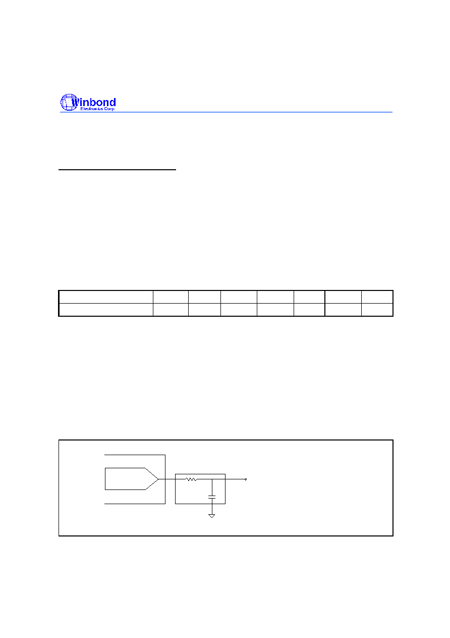
Static DAC application circuit:
Static DAC
Low-pass filter
V
OUTPUT
R
C
T = RC
V
OUTPUT
= V
CC
°—n/255, if T >> T
PWM

Preliminary W78E378/W78C378/W78C374
- 26 -
Three 8-bit Dynamic DACs: DAC8
-
DAC10
The dynamic DACs are especially used to generate parabola waveform for geometric compensation,
or to be used as static DACs. Dynamic DAC application circuit:
Dynamic DAC
V
output
100K
470
+Vsync
0.022u
10u/50V
470
470
10K
10K
4.7u/16V
VDD
The following types of distoration can be compensated:
1. H size distortion:
a. PinCushion Correction (Amplitude)
b. Trapezoid (Keystone)
c. CBOW (Quarter Width)
25%
25%
d. PinCushion Correction (Corner)
e. S Curve
The PCC amplitude can be compensated against V size adjustment automatically.
The Trapzoid can be compensated against V center adjustment automatically.
2. H center distortion:
a. Pin balance (Bow)
b. Key balance (Tilt)
c. Corner balance
Preliminary W78E378/W78C378/W78C374
Publication Release Date: December 1999
- 27 - Revision A1
Sync Processor
Polarity Detector
The H/V polarity is detected automatically and can be known from HPOL bit (HFCOUNTH.7) and
VPOL bit (VFCOUNTH.7).
Fosc
10 MHz
Max. H+V width
(64/Fosc)
◊
62 (counter overflow) = 396.8
µ
S
Max. V width
(2048/Fosc)
◊
2 = 409.6
µ
S
Sync Separator
The Vsync is separated from the composite sync automatically, without any software effort.
Fosc
10 MHz
Min. V width & Max. H width
(1/Fosc)
◊
64 = 6.4
µ
S
Horizontal & Vertical Frequency Counter
There are two 12-bit counters which can count H and V frequency automatically. When VEVENT
(Vsync frequency counter timeout) interrupt happens, the count value values are latched into the
counter registers (HFCOUNTH, HFCOUNTL, VFCOUNTH and VFCOUNTL). And then the S/W may
read the count value (H
COUNT
and V
COUNT
) from the counter registers to calculate the H and V
frequency by the formulas listed below.
V frequency:
The resolution of V frequency counter: V
RESOL
= (1/Fosc)
◊
64.
The V frequency: V
FREQ
= 1/(V
COUNT
◊
V
RESOL
).
The lowest V frequency can be detected: Fosc ˜ 262144. (38.1Hz @Fosc =10 MHz)
H frequency:
The resolution of H frequency counter: H
RESOL
= (1/Fosc)
˜
8.
The H frequency: H
FREQ
= 1/(H
COUNT
◊
H
RESOL
).
The lowest H frequency can be detected: Fosc
˜
512. (19.5 KHz @Fosc = 10 MHz)
Dummy Frequency Generator
The Dummy H and V frequencies are generated for factory burn-in or showing warning message
while there are no input frequency.
(HDUMS1, HDUMS0)
(0, 0)
(0, 1)
(1, 0)
(1, 1)
F
dummyH
Fosc/(8
◊
4
◊
8)
Fosc/(8
◊
2
◊
8)
Fosc/(8
◊
3
◊
8)
Fosc/(8
◊
5
◊
8)
Hsync width
(8
◊
4)/Fosc
(8
◊
2)/Fosc
(8
◊
3)/Fosc
(8
◊
5)/Fosc
VDUMS
0
1
F
dummyV
F
dummyH
/ 512
F
dummyH
/1024
Vsync width
8/ F
dummyH
16/ F
dummyH

Preliminary W78E378/W78C378/W78C374
- 28 -
Hdummy
.....
.....
.....
.....
.....
.....
Vdummy
Vsync width
Hsync width
1/FdummyH
1/FdummyV
For Fosc = 10 MHz:
(HDUMS1,
HDUMS0)
(0, 1)
(1, 0)
(0, 0)
(1, 1)
F
dummyH
78.125 KHz
52.083 KHz
39.063 KHz
31.250 KHz
Hsync width
1.6
µ
S
2.4
µ
S
3.2
µ
S
4.0
µ
S
VDUMS
0
1
0
1
0
1
0
1
F
dummyV
152.6 Hz
76.3 Hz 101.7 Hz 50.9 Hz 76.3 Hz 38.1 Hz 61.0 Hz 30.5 Hz
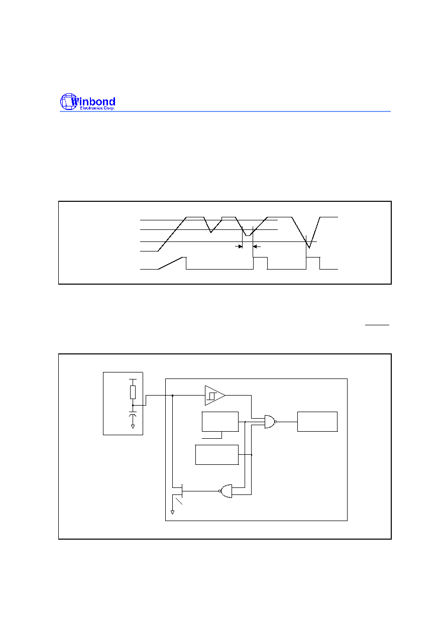
H-clamp Pulse Generator
1. Leading edge/Trailing edge selectable.
* HCES = 0: select leading edge
* HCES = 1: select trailing edge
Negative polarity Hsync
Postive polarity Hsync
(Leading-edge)
(Trailing-edge)
(Leading-edge)
(Trailing-edge)
Hclamp
Hsync
Hsync
Hclamp
Hclamp
Hclamp

Preliminary W78E378/W78C378/W78C374
Publication Release Date: December 1999
- 29 - Revision A1
2. Pulse width selectable.
For Fosc = 10 MHz:
HCWS = 0
HCWS = 1
Pulse Width
500
-
600 nS
900
-
1000 nS
Safe Operation Area (SOA) Interrupt
Upper boundary frequency = F
OSC
/ [8
◊
SOARH]
Lower boundary frequency = F
OSC
/ [8
◊
(SOARL + 1)]
Function description:
∑
If the condition, H
FREQ
lower than the lower boundary freq.
or higher than the upper boundary freq.,
happens twice continuously, the SOAINT will be activated.
∑
If the HIN is stopped for a certain period, the SOAINT will also be generated.
The no Hsync response time is 512/F
OSC
. (e.x., 51.2us for 10 MHz)
∑
If SOAHDIS = 1, then no upper boundary frequency.
Half Hsync Output
When ENHFO (bit 0 of CTRL3) is set, P4.7 (HFO) will output the same or half frequency from P4.0
(HFI). The divide-by-two operation is done at the falling edge of HFI signal when HFO_HALF (bit 3 of
CTRL3) is set. The polarity of HFO is specified by HF_POL (bit 2 of CTRL3).
HFI
HFO
(HFO_HALF=0)
(HF_POL=1)
HFO
(HFO_HALF=0)
(HF_POL=0)
HFO
(HFO_HALF=1)
Preliminary W78E378/W78C378/W78C374
- 30 -
Interrupts
The five interrupt sources are listed as below.
SOURCE VECTOR ADDRESS
DESCRIPTON
PRIORITY WITHIN A LEVEL
1
IE0
0003H
Interrupt 0 edge detected
Highest
2
TF0
000BH
Timer 0 overflow
3
IE1
0013H
Miscellaneous interrupts
*1
4
TF1
001BH
Timer 1 overflow
5
SI1+SI2
002BH
SIO1 or SIO2 interrupt
Lowest
Note: *1: SCLINT + ADCINT + DDC1INT + SOAINT + VEVENT + PARAINT.
The miscellaneous interrupts at vector address 0013H is driven by the following six sources, which
are:
(1) SCLINT: when high-to-low transition on SCL-pin,
(2) ADCINT: when A-to-D conversion completion,
(3) DDC1INT: when DDC1 data byte transmitted (after 9 clock pulses from V
IN
) in the DDC port,
(4) SOAINT: when SOA activated,
(5) VEVENT: on every Vsync pulse or vertical frequency counter overflow,
(6) PARAINT: when parabola timer timeout.
If IE1 interrupt occurs, it is necessary for the programmer to read the INTVECT register to tell where
the interrupt request comes. These sources can be masked individually by clearing their
corresponding bits in the INTMSK register. To clear any of these interrupt flags, just write a '1' to the
corresponding bit in the INTCLR.
The interrupt enable bits and priority control bits for these five main sources are listed as below.
INTERRUPT FLAG
ENABLE BIT
PRIORITY CONTROL BIT
1
IE0
IE.0 & IE.7
IP.0
2
TF0
IE.1 & IE.7
IP.1
3
IE1
IE.2 & IE.7
IP.2
4
TF1
IE.3 & IE.7
IP.3
5
SI+SI2
IE.5 & IE.7
IP.5
Preliminary W78E378/W78C378/W78C374
Publication Release Date: December 1999
- 31 - Revision A1
Bit 0
Bit 1
Bit 4
Bit 3
Bit 2
IE1
IT1
0
1
SCL Interrupt
ADC Interrupt
DDC1 Interrupt
SOA Interrupt
VEVENT Interrupt
PARA Interrupt
INTMSK
INTVECT
SCLINT
ADCINT
DDC1INT
VEVENT
SOAINT
PARAINT
Bit 5
0
2
1
3
4
5
IE0
TF0
TF1
IE
0013H
001BH
002BH
000BH
0003H
IE.3
IE.5
IE.2
IE.1
IE.0
IE.7
IP
IP.0
IP.1
IP.2
IP.3
IP.5
Vector Address
High Priority
Low Priority
Interrupt Polling
Sequence
IE1
SI1+SI2
Preliminary W78E378/W78C378/W78C374
- 32 -
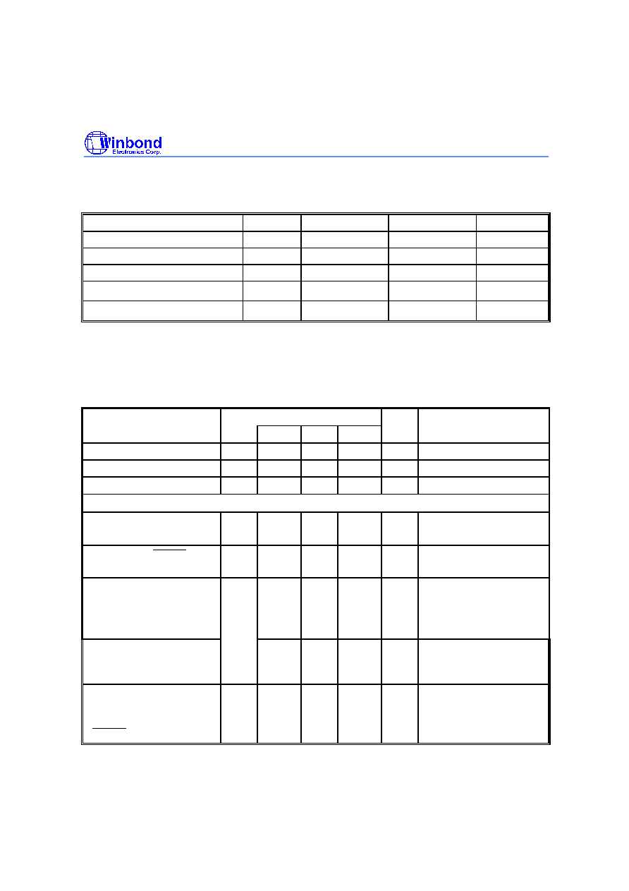
Reset Circuit- Power-low Detector & Watchdog Timer
The reset signals come from the following three sources:
1. External reset input (active low)
2. Power low detect
3. Hardware Watchdog Timer
The power-low detection circuit generates a reset signal once the V
CC
falls below 3.5V for above 10
µ
S or falls below 1.8V, and the reset signal is released after V
CC
goes up to 4.3V.
4.3V
3.8V
1.8V
VCC
Power-low Reset
10uS
The purpose of a watchdog timer is to reset the CPU if the user program fails to reload the watchdog
timer within a reasonable period of time known as the "watchdog interval". The clock source of the
watchdog timer comes from the internal system clock. It can be enabled/disabled by set/clear
WDTEN (bit 5 of CTRL2). For debug purpose, if the WDT reset or power low reset occur, the RESET
pin will be pulled low internally. The pulled-low duration due to WDT reset is about 60/Fosc sec. The
block diagram of the reset circuitry is shown as below.
Watchdog
Timer
Power-low
Supervisor
WDTEN
EN
Reset Logic
R:100K
C:0.01u
External Reset
/RESET
Iol=12mA @Vol=0.45V
Preliminary W78E378/W78C378/W78C374
Publication Release Date: December 1999
- 33 - Revision A1
ELECTRICAL CHARACTERISTICS
Absolute Maximum Ratings
PARAMETER
SYMBOL
MIN.
MAX.
UNIT
DC Power Supply
V
DD
-0.3
+7.0
V
Input Voltage
V
IN
V
SS
-0.3
V
DD
+0.3
V
Input Current
I
IN
-100
+100
mA
Operating Temperature
T
A
0
70
∞
C
Storage Temperature
TST
-55
150
∞
C
Note: Exposure to conditions beyond those listed under Absolute Maximum Ratings may adversely affect the life and reliability of the
device.
D.C. Characteristics
V
DD
-V
SS
= 5V
±
10%, T
A
= 25
∞
C, Fosc = 10 MHz, unless otherwise specified.
PARAMETER
SYM.
SPECIFICATION
UNIT
TEST CONDITIONS
MIN.
TYP. MAX.
Operating Voltage
V
DD
4.5
5
5.5
V
All function must pass!
Operating Current
I
DD
-
-
30
mA
No load, V
DD
= 5.5V
Power-down Current
I
PD
-
-
100
µ
A
No load, V
DD
= 5.5V
Input
Input Current
P2, P3.2
-
P3.4, P4.0
I
IN1
-75
-10
-
-
-10
+10
µ
A
V
DD
= 5.5V, V
IN
= 0V
V
DD
= 5.5V, V
IN
= 5.5V
Input Current RESET
I
IN2
-300
-10
-
-
-100
+10
µ
A
V
DD
= 5.5V, V
IN
= 0V
V
DD
= 5.5V, V
IN
= 5.5V
Input Leakage Current
P1, P2.4
-
P2.7
(
S.F. enabled)
P3.0, P3.1, P3.5
-
P3.7,
P4.4, P4.5 H
IN
, V
IN
I
LK
-10
-
+10
µ
A
V
DD
= 5.5V, 0V<V
IN
<
V
DD
Logical 1-to-0 Transition
Current
P2, P3.2
-
P3.4
I
TL
-650
-
-100
µ
A
V
DD
= 5.5V, V
IN
= 2.0V
Input Low Voltage
P1, P2, P3 (except P3.0 &
P3.1), P4.0, H
IN
, V
IN
,
RESET , OSCIN
V
IL1
0
-
0.8
V
V
DD
= 4.5V
Preliminary W78E378/W78C378/W78C374
- 34 -
D.C. Characteristics, continued
PARAMETER
SYM.
SPECIFICATION
UNIT
TEST CONDITIONS
MIN.
TYP. MAX.
Input Low Voltage
P3.0, P3.1, P4.4, P4.5
V
IL2
0
-
0.3
V
DD
V
V
DD
= 4.5V
Input High Voltage
P1, P2, P3
(except P3.0 &
P3.1), P4.0, H
IN
, V
IN
, RESET
V
IH1
2.0
-
V
DD
+0.2
V
V
DD
= 5.5V
Input High Voltage
P3.0, P3.1, P4.4, P4.5
V
IH2
0.7
V
DD
-
V
DD
+0.2
V
V
DD
= 5.5V
Input High Voltage
OSCIN
V
IH3
3.5
-
V
DD
+0.2
V
V
DD
= 5.5V
Output
Output Low Voltage
P1.0, P1.1, RESET
V
OL1
-
-
0.45
V
V
DD
= 4.5V
I
OL
= +12 mA
Output Low Voltage
P3.0, P3.1, P4.4, P4.5
V
OL2
-
-
0.45
V
V
DD
= 4.5V
I
OL
= +8 mA
Output Low Voltage
P1 (except P1.0 & P1.1)
P2, P3 (except P3.0
-
P3.2)
P4 (except P4.4 & P4.5)
V
OL3
-
-
0.45
V
V
DD
= 4.5V
I
OL
= +4 mA
Output Low Voltage
P3.2, OSCOUT
V
OL4
-
-
0.45
V
V
DD
= 4.5V
I
OL
= +0.8 mA
Output High Voltage
P2, P3.2
-
P3.4
V
OH1
2.4
-
-
V
V
DD
= 4.5V
I
OH
= -100
µ
A
Output High Voltage
P4 (except P4.4 & P4.5)
V
OH2
2.4
-
-
V
V
DD
= 4.5V
I
OH
= -4 mA
Special Function Output
High Voltage
P2.0
-
P2.3, P3.3, P3.4
V
OH3
2.4
-
-
V
V
DD
= 4.5V
I
OH
= -4 mA
Output High Voltage
OSCOUT
V
OH4
2.4
-
-
V
V
DD
= 4.5V
I
OH
= -3 mA
Notes:
*1. RESET has an internal pull-up resistor of about 30 K
.
*2. P2 and P3.2
-
P3.4 can source a transition current when they are being externally driven from 1 to 0. The transition current
reaches its maximum value when V
IN
is approximately 2V.
*3. P3.0, P3.1, P4.4, P4.5, H
IN
, V
IN
and RESET are Schmitt trigger inputs.

Preliminary W78E378/W78C378/W78C374
Publication Release Date: December 1999
- 35 - Revision A1
Appendix A. Application Note for Usage of ADC
To use the ADC, users should pay attention to the following points:
(1) According to the absolute maximum ratings, the input voltage should not exceed V
DD
+0.3V,
especially for the ADC channel pins (P2.4
-
P2.7 & P3.5
-
P3.7). If a voltage over V
DD
+0.3V exists
on any of these ADC channel pins, the AD conversion will fail.
(2) Owing to the CMOS process, the ADC curve of some chip might differ from those of the others.
So, before using the ADC, the S/W should do the ADC calibration described below.
Step 1. Set (ADCS2, ADCS1, ADCS0, ADCcal) = (1, 1, 1, 0) and then do AD coversion to get
the ADC value for the on-chip
0.948V
input. Suppose it is
A
.
Step 2. Set (ADCS2, ADCS1, ADCS0, ADCcal) = (1, 1, 1, 1) and then do AD coversion to get
the ADC value for the on-chip
2.924V
input. Suppose it is
B
.
Step 3. Because the ADC curve in the usable range is linear, any
V
and
X
should
meet the
formula:
(X-A)/(V-0.948) = (B-A)/(2.924-0.948)
,
where
V
is the key voltage (designed by users and thus known) and
X
is its predicted
ADC value. Then, we can get
X = A + (V-0.948)(B-A)/(2.924-0.948)
, regardless of V >
0.948V or < 0.948V. (
Of course, some effort should be paid in S/W to find
X
.)
Step 4. Suppose there are N keys used, the N predicted ADC values for these keys can be
found.
1.0
2.0
3.0
4.0
5.0
ADC input voltage
ADC value
X
A
B
V
Usable range
(is linear)
After finding these N predicted ADC values, the S/W can recognize which key is pressed by
comparing the ADC value of this key with the set of predicted values (found previously).
** Note: To get the exact on-chip calibration voltages (0.948V and 2.924V), the V
DD
should be 5.0V as close as possible.

Preliminary W78E378/W78C378/W78C374
- 36 -
Test strategy before shipping:
(1) Vi = 0V => ADC < 20
(2) Vi = 0.8V => ADC > 25
(3) Vi = 3.2V => ADC < 248
(4) Vi = 4.4V => ADC = 255
(5) 0.8V < Vi < 3.2V, 25 points (step 0.1V) will be tested. All test points should be recognized
correctly.
Comment:
a. (1) guarantees 0V input can be recognized (ADC value < 20).
b. (4) guarantees 5V input can be recognized (ADC value = 255).
c. (2), (3) and (5) guarantee linear (with 4 bits at least) within the usable range (0.8V to 3.2V).
ADC value
Analog voltage (V)
Usable range
0.8
20
25
248
4.4
3.2
Preliminary W78E378/W78C378/W78C374
Publication Release Date: December 1999
- 37 - Revision A1
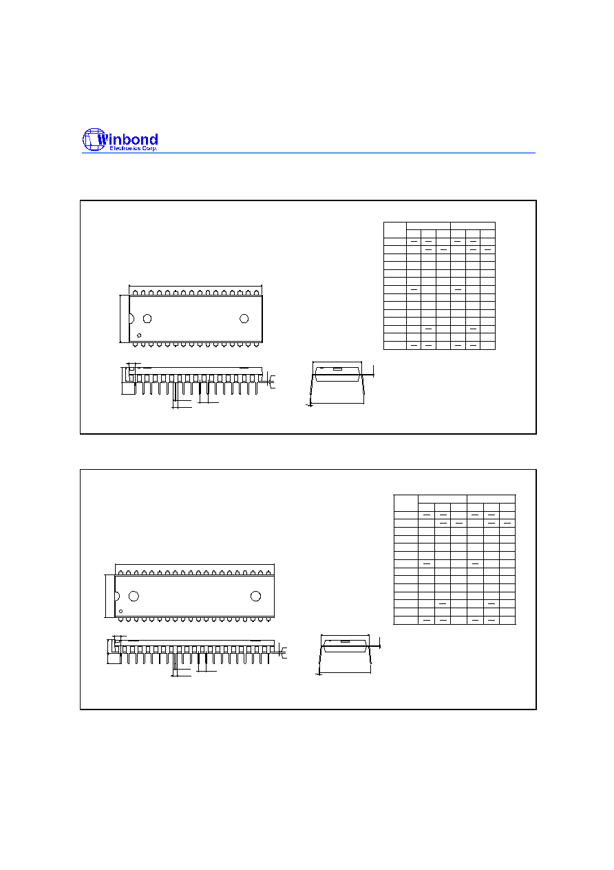
PACKAGE DIMENSIONS
32-pin P-DIP
1. Dimensions D Max. & S include mold flash or
tie bar burrs.
2. Dimension E1 does not include interlead flash.
3. Dimensions D & E1 include mold mismatch and
are determined at the mold parting line.
6. General appearance spec. should be based on
final visual inspection spec.
1.37
1.22
0.054
0.048
Notes:
Symbol
Min. Nom. Max.
Max.
Nom.
Min.
Dimension in inches
Dimension in mm
A
B
c
D
e
A
L
S
A
A
1
2
E
0.050
1.27
0.210
5.33
0.010
0.150
0.016
0.155
0.018
0.160
0.022
3.81
0.41
0.25
3.94
0.46
4.06
0.56
0.008
0.120
0.670
0.010
0.130
0.014
0.140
0.20
3.05
0.25
3.30
0.36
3.56
0.555
0.550
0.545
14.10
13.97
13.84
17.02
15.24
14.99
15.49
0.600
0.590
0.610
2.29
2.54
2.79
0.090
0.100
0.110
B
1
1
e
E
1
a
1.650
1.660
41.91
42.16
0
15
0.085
2.16
0.650
0.630
16.00
16.51
protrusion/intrusion.
4. Dimension B1 does not include dambar
5. Controlling dimension: Inches
15
0
Seating Plane
e
A
2
A
a
c
E
Base Plane
1
A
1
e
L
A
S
1
E
D
1
B
B
32
1
16
17
40-pin DIP
Seating Plane
1. Dimension D Max. & S include mold flash or
tie bar burrs.
2. Dimension E1 does not include interlead flash.
3. Dimension D & E1 include mold mismatch and
are determined at the mold parting line.
6. General appearance spec. should be based on
final visual inspection spec.
.
1.372
1.219
0.054
0.048
Notes:
Symbol
Min. Nom.
Max.
Max.
Nom.
Min.
Dimension in inch
Dimension in mm
0.050
1.27
0.210
5.334
0.010
0.150
0.016
0.155
0.018
0.160
0.022
3.81
0.406
0.254
3.937
0.457
4.064
0.559
0.008
0.120
0.670
0.010
0.130
0.014
0.140
0.203
3.048
0.254
3.302
0.356
3.556
0.540
0.550
0.545
13.72
13.97
13.84
17.01
15.24
14.986
15.494
0.600
0.590
0.610
2.286
2.54
2.794
0.090
0.100
0.110
A
B
c
D
e
A
L
S
A
A
1
2
E
B
1
1
e
E
1
a
2.055
2.070
52.20
52.58
0
15
0.090
2.286
0.650
0.630
16.00
16.51
protrusion/intrusion.
4. Dimension B1 does not include dambar
5. Controlling dimension: Inches.
15
0
e
A
A
a
c
E
Base Plane
1
A
1
e
L
A
S
1
E
D
1
B
B
40
21
20
1
2

Preliminary W78E378/W78C378/W78C374
- 38 -
Package Dimensions, continued
44-pin PLCC
44
40
39
29
28
18
17
7
6
1
L
c
1
b
2
A
H
D
D
e
b
E H
E
y
A
A
1
Seating Plane
D
G
G
E
Notes:
Symbol
Min.
Nom.
Max.
Max.
Nom.
Min.
Dimension in inches
Dimension in mm
y
on final visual inspection spec.
4. General appearance spec. should be based
3. Controlling dimension: Inches
protrusion/intrusion.
2. Dimension b1 does not include dambar
1. Dimension D & E do not include interlead flash.
0.020
0.145
0.026
0.016
0.008
0.648
0.590
0.680
0.090
0.150
0.028
0.018
0.010
0.653
0.610
0.690
0.100
0.050
BSC
0.185
0.155
0.032
0.022
0.014
0.658
0.630
0.700
0.110
0.004
0.51
3.68
0.66
0.41
0.20
16.46
14.99
17.27
2.29
3.81
0.71
0.46
0.25
16.59
15.49
17.53
2.54
1.27
4.70
3.94
0.81
0.56
0.36
16.71
16.00
17.78
2.79
0.10
BSC
16.71
16.59
16.46
0.658
0.653
0.648
16.00
15.49
14.99
0.630
0.610
0.590
17.78
17.53
17.27
0.700
0.690
0.680
A
b
c
D
e
H
E
L
A
A
1
2
E
b
1
H
D
G
G
D
E
Headquarters
No. 4, Creation Rd. III,
Science-Based Industrial Park,
Hsinchu, Taiwan
TEL: 886-3-5770066
FAX: 886-3-5792766
http://www.winbond.com.tw/
Voice & Fax-on-demand: 886-2-27197006
Taipei Office
11F, No. 115, Sec. 3, Min-Sheng East Rd.,
Taipei, Taiwan
TEL: 886-2-27190505
FAX: 886-2-27197502
Winbond Electronics (H.K.) Ltd.
Rm. 803, World Trade Square, Tower II,
123 Hoi Bun Rd., Kwun Tong,
Kowloon, Hong Kong
TEL: 852-27513100
FAX: 852-27552064
Winbond Electronics North America Corp.
Winbond Memory Lab.
Winbond Microelectronics Corp.
Winbond Systems Lab.
2727 N. First Street, San Jose,
CA 95134, U.S.A.
TEL: 408-9436666
FAX: 408-5441798
Note: All data and specifications are subject to change without notice.