
W78C438C
8-BIT MICROCONTROLLER
Publication Release Date: July 1998
- 1 -
Revision A1
GENERAL DESCRIPTION
The W78C438C is a high-performance single-chip CMOS 8-bit microcontroller that is a derivative of
the W78C58 microcontroller family. The W78C438C is functionally compatible with the W78C32,
except that it provides either a 64 KB program/1 MB data memory address or memory-mapped chip
select logic, five general I/O ports, and four external interrupts.
In the W78C32, two I/O ports, Port 1 and Port 3, are available for general-purpose use (Port 3 also
supports alternative functions), and Port 2 and Port 0 are used as the address bus and data bus,
respectively. To enable Port 0 and Port 2 to also be used as general purpose I/O ports, the
W78C438C provides two dedicated address ports (AP5 and AP6) that serve as address output for 64
KB of memory and one address/data port (DP4) that serves as ROM code input and external RAM
data input/output. Unlike the W78C32, this product does not require an external latch device for
multiplexing low byte addresses. The W78C438C also provides four pins (AP7.0
-
AP7.3) to support
either 64 KB program/1 MB data memory space or memory-mapped chip select logic, one parallel I/O
port (Port 8) without bit addressing mode, and two additional external interrupts (
INT2
,
INT3
) .
The W78C438C is programmed in a manner fully compatible with that used to program the W78C32,
except that the external data RAM is accessed by the "MOVX @Ri" instruction. Address paging is
performed by loading page addresses into the HB (high byte) register, which is not a standard register
in the W78C32, before execution of the "MOVX @Ri" instruction.
FEATURES
�
8-bit CMOS microcontroller
�
Fully static design
�
DC to 40 MHz operation
�
ROM-less operation
�
256-byte on-chip scratchpad RAM
�
Either 64 KB program/1 MB data memory address space or 4 memory-mapped chip select pins
�
One 8-bit data/address port
�
Two 8-bit and one 4-bit (optional) address ports
�
Five 8-bit bidirectional I/O ports
-
Four 8-bit bit-addressable I/O ports and one 8-bit parallel I/O port
�
Eight-source, two-level interrupt capability
�
Three 16-bit timer/counters
�
Four external interrupts
�
One full-duplex serial channel
�
Built-in power management
-
Idle mode
-
Power-down mode
�
Packages:
-
84-pin PLCC: W78C438CP-24/40
-
100-pin PQFP: W78C438CF-24/40
W78C438C
- 2 -
PIN CONFIGURATIONS
12
13
14
15
16
17
18
19
20
21
22
23
24
3
3
3
4
3
5
3
6
3
7
3
8
3
9
4
0
60
61
62
63
64
25
26
27
28
29
30
4
1
4
2
4
3
4
4
4
5
4
6
4
7
4
8
4
9
5
0
65
66
67
68
69
70
71
72
73
74
0
1
8
9
1
1
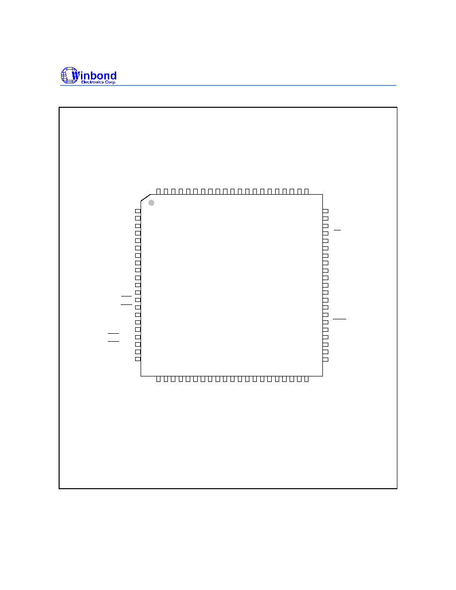
W78C438CP
INT3
P1.5
P1.6
P1.7
RESET
P8.1
P8.0
P8.2
P8.4
P8.5
P8.3
P8.6
P8.7
INT2
RXD, P3.0
VDD
TXD, P3.1
INT0, P3.2
INT1, P3.3
T0, P3.4
T1, P3.5
P
2
.
2
32
31
5
6
7
1
2
3
4
8
4
8
0
8
1
8
2
8
3
7
6
7
7
7
8
7
9
P
0
.
0
P
0
.
1
P
0
.
2
P
0
.
3
D
P
4
.
1
D
P
4
.
0
N
C
V
D
D
N
C
D
P
4
.
2
D
P
4
.
3
D
P
4
.
4
D
P
4
.
5
D
P
4
.
6
D
P
4
.
7
P
1
.
0
P
1
.
1
P
1
.
2
P
1
.
3
P
1
.
4
P
0
.
4
7
5
5
1
59
58
57
55
56
54
5
2
5
3
P
3
.
7
,
/
R
D
X
T
A
L
2
X
T
A
L
1
V
S
S
A
P
7
.
3
,
/
C
S
3
A
P
7
.
2
,
/
C
S
2
N
C
A
P
7
.
0
,
/
C
S
0
A
P
7
.
1
,
/
C
S
1
A
P
6
.
7
A
P
6
.
6
A
P
6
.
5
A
P
6
.
4
A
P
6
.
3
A
P
6
.
2
A
P
6
.
1
A
P
6
.
0
P
2
.
0
P
2
.
1
P
3
.
6
,
/
W
R
P2.4
P2.5
P2.6
P2.7
EA
PSEN
ALE
AP5.7
AP5.6
AP5.5
AP5.4
AP5.3
AP5.2
AP5.1
V
P2.3
AP5.0
P0.7
P0.6
P0.5
V
84-pin PLCC
DD
SS

W78C438C
Publication Release Date: July 1998
- 3 -
Revision A1
Pin Configurations, continued
4
5
6
7
8
9
10
11
12
13
14
15
16
17
1
2
3
18
19
9
20
21
22
23
24
0
1
2
3
3
3
3
4
5
3
3
3
6
3
7
8
3
3
9
0
4
0
25
26
27
28
29
30
4
1
2
3
4
5
6
7
8
9
4
4
4
4
4
4
4
4
5
51
52
53
54
55
56
57
58
59
60
61
62
63
64
65
66
67
68
69
70
71
72
73
74
75
76
77
78
79
80
9
7
8
9
0
1
2
3
4
5
6
7
8
6
5
1
2
3
4
8
8
8
8
8
8
8
8
8
9
9
9
9
9
9
9
9
9
1
0
V
D
D
N
C
P
0
.
3
P
0
.
1
P
0
.
2
P
0
.
0
D
P
4
.
0
D
P
4
.
1
D
P
4
.
2
D
P
4
.
3
D
P
4
.
4
D
P
4
.
5
D
P
4
.
6
D
P
4
.
7
T
2
,
P
1
.
0
P
1
.
2
P
1
.
3
P
1
.
4
N
C
NC
NC
NC
NC
P2.4
P2.5
P2.7
P2.6
V
AP5.7
AP5.6
AP5.5
AP5.4
ALE
AP5.0
PSEN
AP5.1
P0.6
P0.5
P0.4
NC
NC
NC
P0.7
EA
P2.3
AP5.3
AP5.2
NC
V
W78C438CF
X
T
A
L
2
X
T
A
L
1
V
S
S
N
C
P
3 .
7 ,
/
R
D
A
P
7
.
3
,
/
C
S
3
A
P
7
.
2
,
/
C
S
2
A
P
7
.
1
,
/
C
S
1
A
P
6
.
7
A
P
6
.
2
A
P
6
.
1
A
P
6
.
4
A
P
6
.
6
A
P
6
.
3
A
P
6
.
5
A
P
6 .
0
P
2
.
0
P
2
.
1
P
2
.
2
A
P
7
.
0
,
/
C
S
0
NC
NC
NC
NC
NC
P1.7
NC
NC
NC
P1.5
P1.6
P8.0
RESET
P8.1
P8.2
P8.3
P8.4
P8.5
P8.7
P8.6
VDD
RXD, P3.0
TXD, P3.1
T0, P3.4
T1, P3.5
WR, P3.6
INT2
INT3
INT1, P3.3
INT0, P3.2
T
2
E
X
,
P
1
.
1
100-pin PQFP
DD
SS

W78C438C
- 4 -
PIN DESCRIPTION
P0.0
-
P0.7 I/O Port 0
These pins function the same as those in the W78C32, except that a multiplexed address/data bus is
not provided during accesses to external memory.
P1.0
-
P1.7 I/O Port 1
Functions are the same as in the W78C32.
P2.0
-
P2.7 I/O Port 2
Functions are the same as in the W78C32, except that an upper address bus is not provided during
accesses to external memory.
P3.0
-
P3.7 I/O Port 3
Functions are the same as in the W78C32.
DP4.0
-
DP4.7 Data/Address Bus
DP4 provides multiplexed low-byte address/data during access to external memory.
AP5.0
-
AP5.7 Address Bus
AP5 outputs the <7:0> address of the external ROM multiplexed with the <7:0> address of the
external data RAM.
AP6.0
-
AP6.7 Address Bus
AP6 outputs the <15:8> address of the external ROM multiplexed with the <15:8> address of the
external data RAM. During the execution of "MOVX @Ri," the output of AP6 comes from the HB
register, which is the page register for the high byte address, and its address is 0A1H.
AP7.0
-
AP7.3 Address Bus/Chip Select Pins
Set bit 7 of the EPMA (Extended Program Memory Address) register to determine the functions of
port 7. When this bit is "0" (default value), AP7 allows the external memory data to be accessed by
outputting the <19:16> address of the external memory from bits<3:0> of the EPMA register during
the execution of "MOVC A, @A+DPTR" or "MOVX dest, src." At all other times, AP7<3:0> will output
0H.
When this bit is "1," AP7<3:0> (CS3
-
0) are the chip select pins, which support memory-mapped
peripheral device select, and only one pin is active low at any one time. These pins are decoded by
AP6<7:6>. For details, see the table below.
AP6.7
AP6.6
DESCRIPTION
0
0
AP70: low; others: high
0
1
AP71: low; others: high
1
0
AP72: low; others: high
1
1
AP73: low; others: high

W78C438C
Publication Release Date: July 1998
- 5 -
Revision A1
P8.0
-
P8.7 I/O Port
Functions are the same as those of Port 1 in the W78C31, except that they are mapped by the P8
register and not bit-addressable. The P8 register is not a standard register in the W78C32. Its address
is at 0A6H.
INT2
,
INT3
External Interrupt, Input
Functions are similar to those of external
INT0
,
INT1
in the W78C32, except that the functions/status
of these interrupts are determined/shown by the bits in the XICON (External Interrupt Control)
register. The XICON register is bit-addressable but is not a standard register in the W78C32. Its
address is at 0C0H. For details, see the Functional Description below.
EA
External Address, Input
Functions same as W78C32.
RST, XTAL1, XTAL2,
PSEN
, ALE
Functions same as W78C32.
BLOCK DIAGRAM
SFR
RAM
256
Bytes
CPU
Serial
Port
Data Bus
CORE
Interrupt
INT0
Timer0
Timer2
Port 0
Port 1
Port 2
Alternate
Port 8
DP4
AP5
AP6
AP7
Alternate
INT1
Timer1
INT2
INT3
Port 3
Alternate