W78958B
8-BIT EMULATION MICROCONTROLLER
Publication Release Date: September
1997
- 1 -
Revision A3
GENERAL DESCRIPTION
The W78958B is an 8-bit emulation microcontroller that supports emulation for the Winbond W78C51
family of products, including the W78C31, W78C32, W78C51, W78C52, W78C154*, W78C58,
W78C438, and W78C458. It is designed to support real-time (up to 40 MHz) emulation tools, such as
in-circuit emulators (ICEs).
The W78958B is packaged in a 100-pin PQFP and is available in two different types, standard and
advanced. The standard type supports the functions of the W78C31, W78C32, W78C51, W78C52,
W78C154*, and W78C58. The advanced type supports the functions of the W78C438 and W78C458.
Both types can be operated in two modes, normal and emulation. In normal mode, the W78958B runs
freely, like the W78C51 family of products. In emulation mode, which is entered by driving the
ICESET pin high asynchronously, the W78958B stays in the S2 state of the next instruction. In this
mode, the W78958B allows direct access (read/write) to the special function registers (SFRs), the
program counter (PC), and the internal RAM. Also, it allows ICE makers to access the external
program and data memory easily, thereby eliminating the need for glue logic. Moreover, it provides
several signals to facilitate ICE design, including
IPME
(Internal Program Memory Enable), for
switching between "internal" and external ROM, ESEL (Emulation address space Select), for
combining the emulation program and data memory in a 128 KB SRAM, and CLKS1 (internal S1
state clock timing signal), for creating the emulation control signals. Once the ICESET pin goes low,
the W78958B will release its internal clock and return to its normal operating mode.
For detailed specifications concerning the W78C31, W78C32, W78C51, W78C52, W78C154*,
W78C58, W78C438, and W78C458, refer to the Functional Description below or to the Winbond
product specifications.
Notes for all W78C154*:
1. W78958B will emulate W78C154 except port1.6 & port1.7 as output mode:
W78958B
port1.6 & port1.7
pull-ups
W78C154
port1.6 & port1.7
open drain
2. The specification of W78C154 is exclusive, therefore, the DC characteristics is not fully compatible with W78958B,
however
the emulation function is still the same as W78958B.

W78958B
- 2 -
FEATURES
�
8-bit CMOS emulation microcontroller
�
Real-time emulation at up to 40 MHz
�
Convenient emulation chip for ICE market
�
Two types: standard type and advanced type
�
Standard type supports emulation for the W78C31, W78C32, W78C51, W78C52, W78C154*, and
W78C58
�
Advanced type supports emulation for the W78C438, and W78C458
�
In emulation mode, allows direct access to SFRs/PC and internal RAM
�
Allows ICE makers to access external program/data memory easily
�
Supports switching signals between "internal" and external ROM
�
Supports combined emulation program and data memory in a 128 KB SRAM
�
Provides internal S1 state clock timing signal for easy creation of the emulation control signals
�
Fully static design
�
256-byte on-chip scratchpad RAM
�
64 KB program memory address space in standard type; 1 MB extended program memory address
space in advanced type
�
64 KB data memory address space in standard type; 1 MB extended data memory address space in
advanced type
�
Boolean processor
�
Six-source, two-level interrupt capability in standard type; eight-source, two-level interrupt capability
in advanced type
�
Three 16-bit timer/counters
�
One full duplex serial channel
�
Built-in power management
�
Four 8-bit bidirectional and bit-addressable I/O ports in standard type; four 8-bit bidirectional and
bit- addressable I/O ports and one 8-bit bidirectional but parallel I/O port in advanced type
�
Packaged in 100-pin PQFP
-
W78958BF-40
W78958B
Publication Release Date: September 1997
- 3 -
Revision A3
PIN CONFIGURATION
4
5
6
7
8
9
10
11
12
13
14
15
16
17
1
2
3
18
19
20
21
22
23
24
0
1 2
3
3
3
3
4 5
3
3
3
6
3
7 8
3
3
9
0
4
51
52
53
54
55
56
57
58
59
60
61
62
63
64
25
26
27
28
29
30
4
1 2 3
4
5
6
7 8 9
4
4
4
4
4
4
4
4
5
65
66
67
68
69
70
71
72
73
74
75
76
77
78
79
80
9
7
8
9
0
1
2
3
4
5
6
7
8
9
0
6
5
1
2
3
4
8
8
8
8
8
8
8
8
8
9
9
9
9
9
9
9
9
9
1
0
W78958BF
P1.5
P1.6
RESET
ROMS0, P8.0
P8.2
P8.4
P8.5
INT3
P8.3
P8.7
INT2
RXD, P3.0
ICESET
NC
NC
NC
VDD
TXD, P3.1
INT0, P3.2
INT1, P3.3
T0, P3.4
T1, P3.5
WR, P3.6
NC
NC
NC
A
P
7
.
2
,
/
C
S
2
,
/
I
P
M
E
A
P
7
.
0
,
/
C
S
0
,
/
E
W
R
A
P
6
.
7
A
P
6
.
6
A
P
6
.
5
A
P
6
.
4
A
P
6
.
3
A
P
6
.
2
A
P
6
.
1
A
P
6
.
0
P
2
.
0
A
P
7
.
3
,
/
C
S
3
,
/
I
P
S
E
N
P
3
.
7
,
/
R
D
X
T
A
L
2
X
T
A
L
1
V
S
S
N
C
A
P
7
.
1
,
/
C
S
1
,
/
E
R
D
P
2
.
1
P
2
.
2
P
0
.
0
P
0
.
1
P
0
.
2
P
0
.
3
D
P
4
.
1
D
P
4
.
0
N
C
V
D
D
N
C
D
P
4
.
2
D
P
4
.
3
D
P
4
.
4
D
P
4
.
5
D
P
4
.
6
D
P
4
.
7
T
2
,
P
1
.
0
T
2
E
X
,
P
1
.
1
P
1
.
2
P
1
.
3
P
1
.
4
NC
P2.3
P2.4
P2.5
P2.6
P2.7
EA
NC
PSEN
ALE
AP5.7
AP5.6
AP5.5
AP5.4
AP5.3
AP5.2
AP5.1
VSS
NC
NC
NC
AP5.0
P0.7
P0.6
P0.5
P0.4
NC
ENSTD
ESEL
CLKS1
P1.7
ROMS0, P8.1
(100-pin PQFP)
EMU
P8.6
W78958B
- 4 -
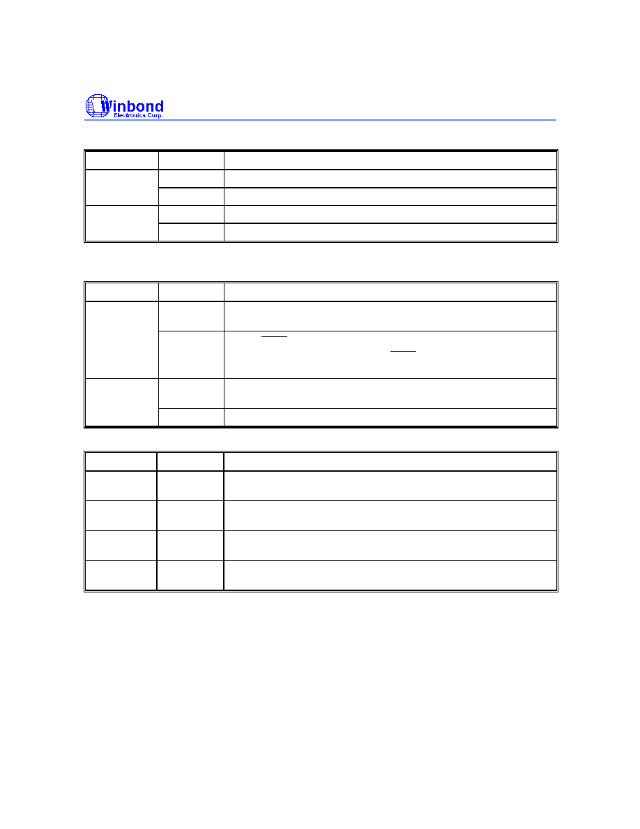
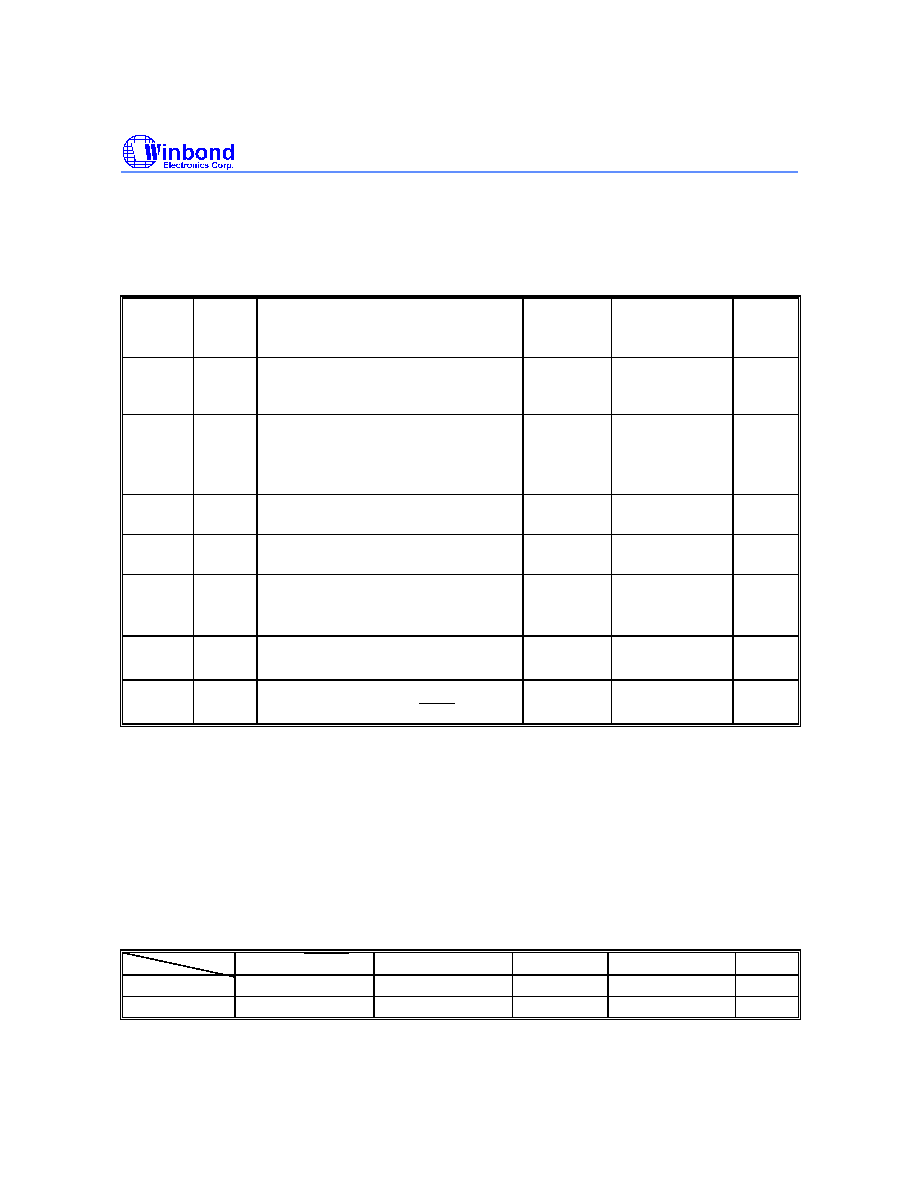
PIN DESCRIPTION
ENSTD Enable Standard Type, Input, Active Low
TYPE
MODE
DESCRIPTION
Advanced
-
Default status is pulled high by internal pull-up resistor.
Standard
-
A low on this pin enables the standard type.
Note: "-" in "Mode" column means that the function description is valid in both modes, normal and emulation.
EA External Address, Input
TYPE
MODE
DESCRIPTION
Advanced
-
Functions same as in W78C438.
Standard
-
Functions same as in W78C51, W78C52, W78C154* or W78C58.
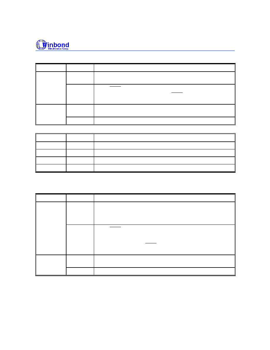
PSEN
TYPE
MODE
DESCRIPTION
Advanced
Normal
Functions same as in W78C438.
Emulation
In high impedance state.
Standard
Normal
Pins ROMS1 and ROMS0 determine the function of PSEN. For
details, see Table D1 below.
Emulation
In high impedance state.
ROMS1
ROMS0
FUNCTION of PSEN, PORT 0, AND PORT 2
0
0
Same as in the W78C51 (verify 4K ROM).
0
1
Same as in the W78C52 (verify 8K ROM).
1
0
Same as in the W78C154* (verify 16K ROM).
1
1
Same as in the W78C58 (verify 32K ROM).
Table D1.
ALE
TYPE
MODE
DESCRIPTION
Advanced
Normal
Functions same as in W78C32.
Emulation
In high impedance state.
Standard
Normal
Functions same as in W78C52.
Emulation
In high impedance state.
W78958B
Publication Release Date: September 1997
- 5 -
Revision A3
RST, XTAL1, XTAL2
TYPE
MODE
DESCRIPTION
Advanced
-
Functions same as in W78C32.
Standard
-
Functions same as in W78C52.
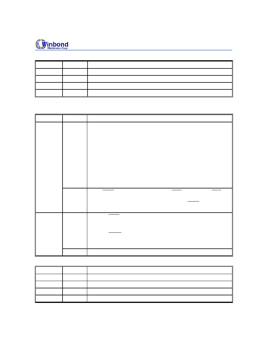
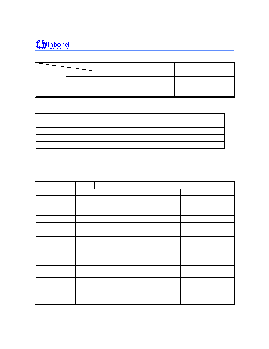
P0.7
-
P0.0 Port 0, Bits 7
-
0
TYPE
MODE
DESCRIPTION
Advanced
Normal
Functions are the same as those in the W78C32, except that a
multiplexed address/data bus is not provided during accesses to
external memory.
Emulation
Frozen in the original state.
Standard
Normal
Pins ROMS1 (P8.1) and ROMS0 (P8.0) determine functions of P0.7
-
P0.0. For details, see Table D1.
Emulation
When
ESEL
is held at "H" level, P0.7
-
P0.0 are floating.
P1.7
-
P1.0 Port 1, Bits 7
-
0
TYPE
MODE
DESCRIPTION
Advanced
Normal
Functions are the same as those in the W78C32.
Emulation
Frozen in the original state.
Standard
Normal
Functions are the same as those in the W78C52.
Emulation
Frozen in the original state.
P2.7
-
P2.0 Port 2, Bits 7
-
0
TYPE
MODE
DESCRIPTION
Advanced
Normal
Functions are the same as those in the W78C32, except that a high-
byte address bus is not provided during accesses to external
memory.
Emulation
Frozen in the original state.
Standard
Normal
Pins ROMS1 and ROMS0 determine functions of P2.7
-
P2.0. For
details, see Table D1.
Emulation
When
ESEL
is held at "H" level, the states of P2.7
-
P2.0 depend on
the MP2 (Mask Port 2) register. At this time, if the bit content of MP2
is 0, the corresponding pin of Port 2 maintains in the original state;
otherwise, the corresponding pin of Port 2 is in high impedance state.
W78958B
- 6 -
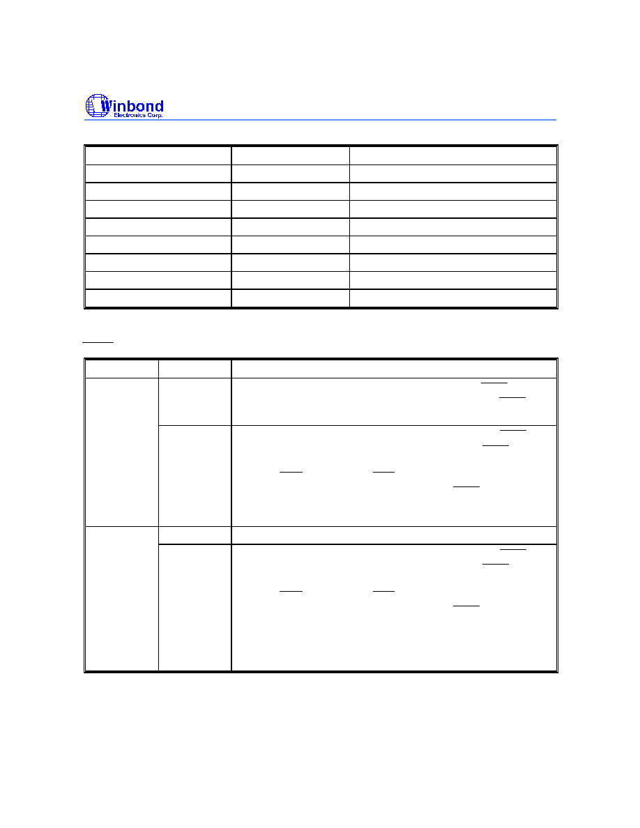
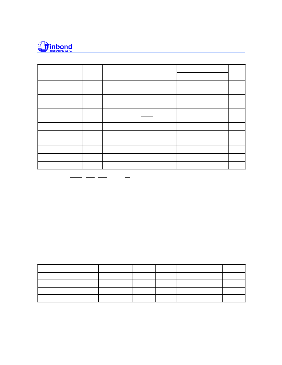
P3.7
-
P3.0 Port 3, Bits 7
-
0
TYPE
MODE
DESCRIPTION
Advanced
Normal
Functions are the same as those in the W78C32.
Emulation
Frozen in the original state.
Standard
Normal
Functions are the same as those in the W78C52.
Emulation
Frozen in the original state.
DP4.7
-
DP4.0 Address/Data Bus, Bits 7
-
0
TYPE
MODE
DESCRIPTION
Advanced
Normal
DP4 provides a multiplexed low-byte address/data bus during
accesses to external memory.
Emulation
When ESEL is held at "L" level, DP4 is the data input/output of the
SFR/PC and internal RAM. When ESEL is held at "H" level, DP4 is
in high impedance state.
Standard
Normal
Pins ROMS1 and ROMS0 determine functions of DP4. For details,
see Table D2.
Emulation
Same as in the advanced type.
ROMS1
ROMS0
FUNCTIONS OF DP4
0
0
Provides a multiplexed low-byte address/data bus during accesses to
external 4 KB EPROM.
0
1
Provides a multiplexed low-byte address/data bus during accesses to
external 8 KB EPROM.
1
0
Provides a multiplexed low-byte address/data bus during accesses to
external 16 KB EPROM.
1
1
Provides a multiplexed low-byte address/data bus during accesses to
external 32 KB EPROM.
Table D2.
W78958B
Publication Release Date: September 1997
- 7 -
Revision A3
AP5.7
-
AP5.0 Address Bus, Bits 7
-
0
TYPE
MODE
DESCRIPTION
Advanced
Normal
AP5<7:0> output the <7:0> address of the external ROM multiplexed
with the <7:0> address of the external data RAM.
Emulation
When ESEL is held at "L" level, AP5 is the low-byte address input for
the SFR/PC and internal RAM. When ESEL is held at "H" level, AP5
is in high impedance state.
Standard
Normal
Pins ROMS1 and ROMS0 determine functions of AP5. For details,
see Table D3.
Emulation
Same as in the advanced type.
ROMS1
ROMS0
FUNCTIONS of AP5
0
0
AP5 output the <7:0> address of the external 4K EPROM.
0
1
AP5 output the <7:0> address of the external 8K EPROM.
1
0
AP5 output the <7:0> address of the external 16K EPROM.
1
1
AP5 output the <7:0> address of the external 32K EPROM.
Table D3.
AP6.7
-
AP6.0 Address Bus, Bit 15
-
8
TYPE
MODE
DESCRIPTION
Advanced
Normal
AP6<7:0> output the <15:8> address of the external ROM
multiplexed with the <15:8> address of the external data RAM.
During the execution of "MOVX @Ri," AP6's output comes from the
HB register, which is the page register for the high byte address.
Emulation
When ESEL is held at "L" level, AP6<0> is the address input for the
accesses to the SFR/PC and internal RAM. At this time, if AP6<0> =
0, the SFR/PC can be accessed; if AP6<0> = 1, the internal RAM
can be accessed. When ESEL is held at "H" level, AP6 is in high
impedance state.
Standard
Normal
Pins ROMS1 and ROMS0 determine functions of AP6. For details,
see Table D4.
Emulation
Same as in the advanced type.
W78958B
- 8 -
ROMS1
ROMS0
FUNCTIONS OF AP6
0
0
AP6<3:0> output the <11:8> address of the external 4K EPROM.
0
1
AP6<4:0> output the <12:8> address of the external 8K EPROM.
1
0
AP6<5:0> output the <13:8> address of the external 16K EPROM.
1
1
AP6<6:0> output the <14:8> address of the external 32K EPROM.
Table D4.
AP7.3
-
AP7.0 Address Bus, Bit 3
-
0, Input/Output, Dual-purpose
TYPE
MODE
DESCRIPTION
Advanced
Normal
Bit 7 of EPMA (Extended Program Memory Address) register
determines functions of AP7<3:0>.
When this bit is "0" (default value), AP7 outputs the <19:16> address of
the external ROM from bits <3:0> of EPMA register during the
execution of "MOVC A,@A+DPTR" to read the external ROM data, the
execution of "MOVX A,@DPTR" to read the external RAM data, or the
execution of "MOVX @DPTR,A" to write the external RAM data.
Excluding those times, AP7<3:0> output 0H.
When this bit is "1," AP7<3:0> (CS3
-
0) are the output pins to support
memory-mapped peripheral chip select, and only one of them is active
low at any time. These pins are decoded by AP6<7:6>. For details, see
Table D5.
Emulation
When ESEL is held in "L" state, AP7<0> (EWR) and AP7<1> (ERD)
are the write and read control input signals, respectively, for the
accesses to the SFR/PC and internal RAM. When ESEL is held in "H"
state, AP7<3:0> are in high impedance state.
Standard
Normal
AP7<2> (
IPME
) is the "internal" program memory enable signal. It
outputs "0" to indicate that the access buses are DP4, AP5 and AP6. It
outputs "1" to indicate that the access buses are Port 0 and Port 2.
AP7<3> (
IPSEN
) is the "internal" program store output enable signal. It
outputs "0" to enable the "internal" program memory onto the DP4
address/data bus during fetch and MOVC operations.
Emulation
Same as in the advanced type.
AP6.7
AP6.6
DESCRIPTION
0
0
AP7.0: low; others: high
0
1
AP7.1: low; others: high
1
0
AP7.2: low; others: high
1
1
AP7.3: low; others: high
Table D5.

W78958B
Publication Release Date: September 1997
- 9 -
Revision A3
P8.7
-
P8.0 Port 8, Bits 7
-
0, Input/Output
TYPE
MODE
DESCRIPTION
Advanced
Normal
Functions are the same as those of Port 1 in the W78C31, except
that they are mapped by the P8 register and not bit-addressable. The
P8 register is not a standard register in the W78C32. Its address is at
0A6H.
Emulation
Frozen in the original state.
Standard
Normal
P8.1 (ROMS1, standard type ROM size Select 1) and P8.0 (ROMS0)
are the input pins that determine which of four different ROM sizes is
being used: 4K, 8K, 16K, or 32K bytes. For details, see Table D1
-
D4.
Emulation
Frozen in the original state.
INT2 and INT3 External Interrupt 2 and 3, Input
TYPE
MODE
DESCRIPTION
Advanced
Normal
Functions are similar to those of external interrupt 0 and 1 in the
W78C31, except that the functions/status of these interrupts are
determined/shown by the bits in the XICON (External Interrupt
Control) register. For details, see Table D6. The XICON register is
bit-addressable but is not a standard register in the W78C32. Its
address is at 0C0H. The interrupt vector addresses and the priority
polling sequence within the same level are shown in Table D7.
Emulation
Frozen in the original state.
Standard
-
Not supported.
BIT
ADDR.
NAME
FUNCTION
7
0C7H
PX3
High/low priority level for
INT 3
is specified when this bit is
set/cleared by software.
6
0C6H
EX3
Enable/disable interrupt from INT3 when this bit is set/cleared by
software.
5
0C5H
IE3
If IT3 is "1," IE3 is set/cleared automatically by hardware when
interrupt is detected/serviced.
4
0C4H
IT3
INT3 is falling-edge/low-level triggered when this bit is set/cleared by
software.
3
0C3H
PX2
High/low priority level for
INT 2
is specified when this bit is
set/cleared by software.
2
0C2H
EX2
Enable/disable interrupt from
INT 2
when this bit is set/cleared by
software.
1
0C1H
IE2
If IT2 is "1," IE2 is set/cleared automatically by hardware when
interrupt is de0tected/serviced.
0
0C0H
IT2
INT 2
is falling-edge/low-level triggered when this bit is set/cleared
by software.
Table D6. Functions of XICON Register.
W78958B
- 10 -
INTERRUPT SOURCE
VECTOR ADDRESS
PRIORITY SEQUENCE WITHIN LEVEL
External Interrupt 0
03H
0 (Highest)
Timer/Counter 0
0BH
1
External Interrupt 1
13H
2
Timer/Counter 1
1BH
3
Serial Port
23H
4
Timer/Counter 2
2BH
5
External Interrupt 2
33H
6
External Interrupt 3
3BH
7 (Lowest)
Table D7.
ESEL Emulation Address Space Select, Input/Output, Dual-purpose
TYPE
MODE
DESCRIPTION
Advanced
Normal
While the W78958B is accessing program memory, ESEL outputs
"0." While the W78958B is accessing data memory, the ESEL
outputs "1."
Emulation
Default status is pulled low by internal pull-high resistor. ESEL is
used to select two emulation address spaces. When ESEL is held
in "L" state, the SFR/PC and internal RAM can be accessed, and
AP7<0>(EWR) and AP7<1>(ERD) are the active low write and
read control input signals, respectively. When ESEL is held in "H"
state, the external ROM and RAM can be accessed (P3.6 and P3.7
are weakly pulled high by internal pull-high resistors).
Standard
Normal
Same as in the advanced type.
Emulation
Default status is pulled low by internal pull-high resistor. ESEL is
used to select two emulation address spaces. When ESEL is held
in "L" state, the SFR/PC and internal RAM can be accessed, and
AP7<0>(EWR) and AP7<1>(ERD) are the active low write and
read control input signals, respectively. When ESEL is held in "H"
state, the external ROM/RAM can be accessed (P3.6/P3.7 are
weakly pulled high by internal pull-high resistors), P0.7
-
P0.0 are
floating, and P2.7
-
P2.0 are in high impedance state optionally
dependent on the content of register MP2.
W78958B
Publication Release Date: September 1997
- 11 -
Revision A3
ICESET Emulation Mode Enable, Input, Active High
This pin, which is used to facilitate ICE applications, is default low with an internal pull-low resistor.
When ICESET is set active, the W78958B will enter the emulation mode. In this mode, the
W78958B's internal clock and states are frozen, but the oscillator continues to run. The contents of
the SFRs, PC, the 256-byte internal RAM, and the external program/data memory can then be
accessed easily by ICE makers to eliminate board-level glue logic. As soon as the ICESET pin goes
low again, the W78958B will release the internal clock and return to its original operating mode.
EMU Emulation Mode Active Indicator, Output, Active High
When ICESET is set to high and synchronized with the internal clock, EMU will go high at the end of
the S1 state of the next instruction. This pin indicates that the W78958B has entered the emulation
mode after ICESET acknowledgment. When ICESET is set to low, the W78958B clears the content of
IR (00H is the opcode of instruction NOP), and then leave the emulation mode. At this time, the
W78958B runs a NOP instruction to prevent improper code from being executed, because the
content of PC may have been changed. After the W78958B leaves the emulation mode
-
i.e., the
internal clock and states start to run
-
it takes four states to fetch the second (ignored) byte of NOP.
EMU will go low until the complete NOP instruction has been finished
-
that is, it will go low at the end
of the S4 state. EMU goes low four states after the device exits the emulation mode.
CLKS1 Machine Cycle Clock output pin
CLKS1 outputs the internal S1 state cycle clock.
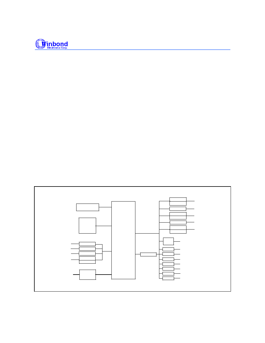
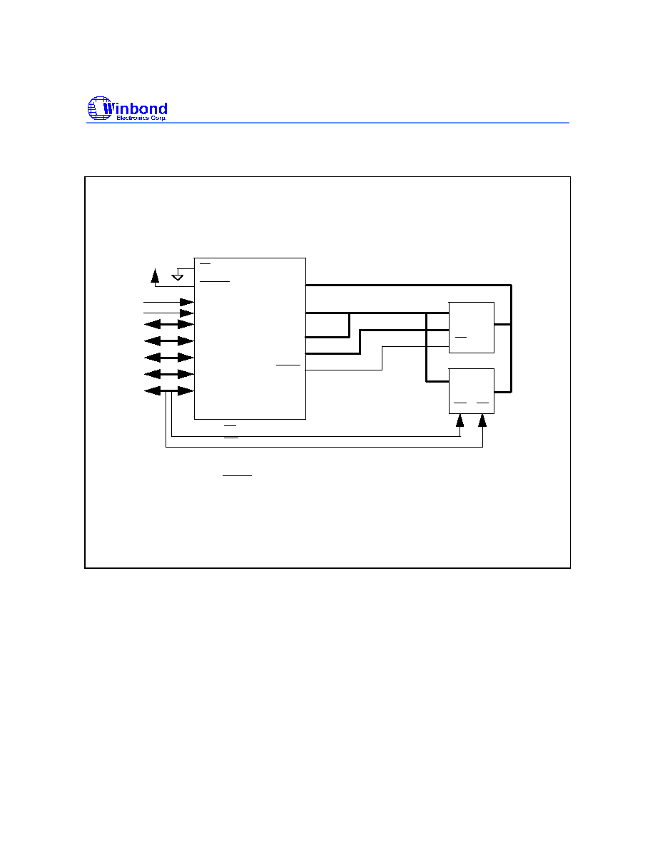
BLOCK DIAGRAM
SFR
RAM
256
Bytes
CPU
Port 0
Port 1
Port 2
Port 3
Serial
Port
Data Bus
CORE
Emulation
Type select
Interrupt
Timer0
Timer1
INT0
INT1
Timer2
logic
INT2
INT3
DP4
AP5
AP6
AP7
Port 8
Alternate
Alternate
Alternate
Alternate
Note: AP7, Port 8, INT2 and INT3 are valid only in advanced type.

W78958B
- 12 -
FUNCTIONAL DESCRIPTION
The W78958B is available in two types, an advanced type and a standard type, which are intended
for use with different end products. The default product type is the advanced type. Both the advanced
type and the standard type are also available with an emulation function. To configure the W78958B
to operate as the advanced type or standard type and to enter the emulation mode, adjust the input
pin settings as shown in the table below. (Note that a transition between the advanced type and
standard type is not permitted after power-on.)
Advanced
Emulation
Standard
Emulation
Notes
ENSTD
EA
ICESET
EMU
I
I
I
O
High
Low
Low High
Low High
Low
High/Low
Low High
Low High
1
2
Notes:
1. This pin is pulled high internally.
2. This pin is pulled low internally.
The type transition diagram for the advanced and standard types is shown below:
STANDARD
TYPE
EMULATION
ICESET = 1
ICESET = 0
ADVANCED
TYPE
EMULATION
ICESET = 1
ICESET = 0
ENSTD =1
EA = 0
POWER ON
ENSTD =1
Figure E. 1
Note that a transition between the advanced type and standard type is not permitted after power-on.
Advanced Type, Normal Mode
At power-on, if
ENSTD
is set to high or left floating and
EA
is set to low, then the W78958B will
operate as the advanced type. The advanced type provides four general-purpose I/O ports for
W78C32 applications; the address and data bus are separated from Port 0 and Port 2 so that these
ports can be used as general-purpose I/O ports. In this type, DP4 is the data bus for external program
and data memory, AP5<7:0> are the low byte address, AP6<7:0> are the high byte address,
PSEN
enables the external program memory to DP4, and P3.6 (
WR
) and P3.7(
RD
) are the write and read
control signals for the external data memory, respectively. The external latch for multiplexing the low

W78958B
Publication Release Date: September 1997
- 13 -
Revision A3
byte address is no longer needed in this type. The advanced type supports 64 KB of external program
memory and 64 KB of external data memory, just as a W78C32 does.
The programming of the advanced type is fully compatible with that of the W78C32 except that the
external data RAM is accessed by a "MOVX @Ri" instruction. To support address paging, there is an
additional 8-bit SFR "HB" (high byte), which is a nonstandard register, at address 0A1H. During the
execution of "MOVX @Ri," the contents of HB are output to AP6. The page address is modified by
loading the HB register with a new value before execution of the "MOVX @Ri" instruction. To
read/write the HB register, one can use the "MOV direct" instruction or "read-modify-write"
instructions. The HB register does not support bit-addressable instructions.
The advanced type provides four pins, AP7.3
-
AP7.0 (CS3
-
CS0), to support either 1 MB
program/data memory space or memory-mapped chip select logic. Bit 7 of EPMA (Extended Program
Memory Address) register determines the functions of these pins. When this bit is "0" (default value),
AP7<3:0> support external program and data memory addresses up to 1 MB for applications that
require additional external memory to store large amounts of data. During the execution of "MOVC
A,@A+DPTR" to read the external ROM data, the execution of "MOVX @DPTR,A" to write the
external RAM data, or the execution of "MOVX A,@DPTR" to read the external RAM data, AP7<3:0>
output address <19:16> from bits <3:0> of the EPMA (Extended Program Memory Address) register.
Excluding that time, AP7<3:0> always output 0H to ensure the instruction fetch is within the 64K
program memory address. Different banks can be selected by modifying the content of the EPMA
register before the execution of these instructions.
When EPMA.7 is "1," AP7<3:0> are output pins that support the memory-mapped peripheral chip
select logic, which eliminates the need for glue logic. These pins are decoded by AP6<7:6>. Only one
of the pins is active low at any one time. That is, they are active individually with 16 K address
resolution. For example, CS0 is active low for the address range from 0000H to 3FFFH, CS1 is active
low for 4000H to 7FFFH, and so forth.
The EPMA register is a nonstandard 8-bit SFR at address 0A2H in the W78C32. To read/write the
EPMA register, one can use the "MOV direct" instruction or "read-modify-write" instructions. Bits
<6:4> of the EPMA register are reserved bits, and their output values are 111B if they are read. The
content of EPMA is 70H after RESET. The EPMA register does not support bit-addressable
instructions.
The advanced type provides one parallel I/O port, Port 8. Its function is the same as that of Port 1 in
the W78C31, except that the port is mapped by the P8 register and is not bit-addressable. The P8
register is not a standard register in the W78C32. Its address is at 0A6H. To read/write the P8
register, one can use the "MOV direct" instruction or "read-modify-write" instructions.
The advanced type provides two additional external interrupts,
INT 2
and
INT 3
, whose functions are
similar to those of external interrupt 0 and 1 in the W78C31. The functions/status of these interrupts
are determined/shown by the bits in the XICON (External Interrupt Control) register. For details, see
Table D6. The XICON register is bit-addressable but is not a standard register in the W78C32. Its
address is at 0C0H. To set/clear the bits of the XICON register, one can use the "SETB (or CLR) bit"
instruction. For example, "SETB 0C2H" sets bit EX2 of XICON. The interrupt vector addresses and
the priority polling sequence within the same level are shown in Table D7.
For a description of the emulation functions of the advanced type, refer to the section below on the
emulation functions.

W78958B
- 14 -
Standard Type, Normal Mode
If
ENSTD
is set to low at power-on, then the W78958B will operate as the standard type. In this type,
pins ROMS1 and ROMS0 are input pins that are used to select one of four different ROM sizes: 4, 8,
16, or 32 K bytes. When EA is set to high, an internal program code is fetched from the external 4, 8,
16, or 32 KB EPROM, depending on the state of ROMS1 and ROMS0. The interface pins needed are
DP4<7:0>, as the data bus, and AP5<7:0> and AP6<3:0>, AP6<4:0>, AP6<5:0> or AP6<6:0>, as the
address bus, again depending on the state of ROMS1 and ROMS0. When
EA
is set to low, the
device is compatible with W78C32 operations.
For example, when pins ROMS1 and ROMS0 are held in "L" and "H" states, respectively, the
functions of the standard type are fully compatible with those of the W78C52, except that the internal
8 KB ROM is replaced by an external EPROM. To reduce the size of the EPROM, one can use the
W78T064, a 20-pin, 300-mil 8 KB EPROM with internal address latch. If the W78T064 is used as the
EPROM, DP4<7:0> should be used as the low-byte address and data bus. And the AP7<3> (
IPSEN
)
enables the "internal" (lower-order 8 KB, for this example) program memory output onto the DP4
address/data bus during fetch and MOVC operations. For detailed specifications concerning the
W78T064, refer to the W78T064 product specifications.
The
IPME
pin indicates the access buses for the program memory. During accesses to the "internal"
program memory, it outputs "0" to indicate that the access buses are DP4, AP5, and AP6. During
accesses to the "external" program memory, it outputs "1" to indicate that the access buses are Port 0
and Port 2.
For a description of the emulation functions of the standard type, refer to the next section.
Emulation Functions (Both Types)
The W78958B supports emulation functions for the standard type (emulation of the W78C31,
W78C32, W78C51, W78C52, W78C154*, and W78C58) and the advanced type (emulation of the
W78C438, and W78C458).
When the device is operating in the normal mode, pins
ESEL
, CLKS1, AP7<2> (
IPME
), ROMS1 and
ROMS0 provide special functions to facilitate ICE design. When the emulation program and data
memory are combined in a single chip,
ESEL
is used to separate the two memory spaces.
ESEL
outputs "0" to indicate that the W78958B is accessing program memory and "1" to indicate that the
W78958B is accessing data memory. CLKS1 outputs the internal S1 state cycle clock, which can be
used as a base for the necessary timing signals. When W78958B is operating as the standard type
and emulates a model that includes an internal ROM, AP7<2> (
IPME
) is used to select the "internal"
or external program memory. When the W78958B fetches the "internal" program,
IPME
outputs "0"
to indicate that the access buses are DP4, AP5, and AP6. When the W78958B fetches the external
program,
IPME
outputs "1" to indicate that the access buses are Port 0 and Port 2. Finally, in the
standard type,
PSEN
, Port 0, Port 2, DP4, AP5, and AP6 are used to configure the device to emulate
products with different ROM code sizes, such as the W78C51 (4 KB ROM), W78C52
�]
8 KB ROM),
W78C154* (16 KB ROM), and W78C58 (32 KB ROM). Pins ROMS1 and ROMS0 are used to select
the ROM size. Concerning the functions of
PSEN
, Port 0, Port 2, DP4, AP5, and AP6, see tables D1
to D4.
In an ICE system, when a breakpoint condition is met or the user forces the CPU to stop running, the
W78958B's ICESET pin is forced high by the system operation. When ICESET active is sampled at
the end of the S1 state, the EMU pin is set to high to indicate that the W78958B has entered the
emulation mode. Once this occurs, the W78958B will remain in the S2 state of the instruction

W78958B
Publication Release Date: September 1997
- 15 -
Revision A3
currently specified by the breakpoint. In this mode, all internal clocks are stopped and the primary I/O
pins of the W78958B are frozen in their previous states; only the oscillator continues to run. Also, the
contents of all the SFRs/PC and the scratchpad RAM remain as they were at the end of the last
instruction.
When the device is in the emulation mode, the internal SFR/PC/RAM can be accessed directly, and
the external ROM/RAM can also be accessed easily. The
ESEL
input is used to separate the two
access spaces (the internal SFR/PC/RAM and the external ROM/RAM). To access the internal
SFR/PC/RAM, hold
ESEL
at "L" level. DP4 then serves as a bidirectional data bus, AP5 and AP6<0>
as the address input bus, and AP7<0>/AP7<1> as the write/read control input signals, When AP6<0>
is "0," the SFR/PC can be accessed; when AP6<0> is "1," the internal RAM can be accessed. The
SFRs' addresses are the same as those specified in the W78C32. The HB (0A1H), EPMA (0A2H), P8
(0A6H), and XICON (0C0H) registers can be accessed only in the advanced type. The addresses of
the PC's low-byte (PCL) and high-byte (PCH) are 0A3H and 0A4H, respectively, which are not the
standard SFRs in the W78C32 and cannot be accessed in normal mode.
When
ESEL
is held at "H" level, DP4, AP5, AP6, and AP7 are in high impedance state, but the
functions of Port 0 and Port 2 depend on the type of W78958B. In the advanced type, Port 0 and Port
2 are in the original state. In the standard type, Port 0 is floating, and the individual bits of Port 2 are
either in the original state or in high impedance state, depending on the contents of the MP2 (Mask
Port 2) register. If the content of a particular bit in MP2 is "0," the corresponding pin of Port 2 is in the
original state; if the content of a particular bit in MP2 is "1," the corresponding pin of Port 2 is in the
high impedance state. For example, when 16 KB external program/data memory is needed and the
remaining two pins, P26 and P27, are used as the I/O, MP2 must be filled with 3FH before the
external program/data memory can be accessed. The MP2 register is a nonstandard 8-bit SFR at
address 0A5H in the W78C32, and its default value is 0FFH. It can be accessed only in the emulation
mode of the standard type.
After the W78958B enters the emulation mode, the code located on the breakpoint address is filled
into the IR register but is not decoded, and the content of PC is incremented by one. The content of
PC may be modified during the emulation mode, but the code within IR will not be modified
accordingly. For this reason, the W78958B clears the content of IR (00H is the opcode of instruction
NOP) before leaving the emulation mode. The emulation mode can be released by resetting the
ICESET pin to low. After the signal is acknowledged, the W78958B clears the content of IR, and then
the W78958B will resume operation from the S2 state. At this time, the W78958B runs an NOP
instruction to prevent improper code from being executed, because the content of PC may have been
changed. After the W78958B leaves the emulation mode, i.e., the internal clock and states start to
run, it takes four states to fetch the second (ignored) byte of NOP. EMU will go low until the complete
NOP instruction has been finished; that is, it will go low at the end of the S4 state. EMU goes low four
states after the device exits the emulation mode. For more information, see the Timing Diagram for
the emulation cycle.
The content of PC must be handled carefully. For example, if the W78958B enters emulation mode
after the content of PC has reached a user-defined breakpoint address, say 100H, the content of PC
will be incremented by 1, to 101H. To restart the program from the same address (100H) after the
device exits the emulation mode, 1 must be subtracted from the content of PC
-
that is, 100H must be
filled into PC before the device exits emulation mode. To restart the program from a new program
address (for example, 200H) after leaving the emulation mode, fill the new address value (200H) into
PC. If one breakpoint is set in the current PC, this breakpoint will be reached again after leaving the
emulation mode, however, so this breakpoint must be avoided carefully.
W78958B
- 16 -
It is important that the W78958B not enter emulation mode after entering power-down mode, even if
the ICESET pin goes high. If the breakpoint address is the instruction that immediately follows
activation of the idle mode, the EMU pin will go high after the execution of the interrupt service
routine while the W78958B is being awakened from interrupt.
New Special Function Registers
NAME
ADDR
OBJECT
VALUE
AFTER
RESET
TIME TO
ACCESS
NOTES
HB
A1
During the execution of "MOVX
@Ri," the content of HB is output to
AP6.
00H
Both modes for
advanced type
1
EPMA
A2
EPMA.7 determines functions of
AP7.
EPMA.3
-
EPMA.0 determine values
of AP7<3:0> when EPMA.7 is "0."
70H
Both modes for
advanced type
1
PCL
A3
Accessed by ICE makers.
00H
Emu. mode for
both types
PCH
A4
Accessed by ICE makers.
00H
Emu. mode for
both types
MP2
A5
The bits of MP2 determine functions
of P2<7:0> during the emulation
mode for standard type.
0FFH
(for POR
only)
Emu. mode for
Ver. type
2
P8
A6
The content of P8 is output to port 8.
0FFH
Both modes for
advanced type
1
XICON
C0
The bits of XICON determine/show
the functions/status of
INT 2
-
3.
00H
Both modes for
advanced type
1
Notes:
1. The instructions used to access these nonstandard registers may cause assembling errors with respect to the 2500 A. D.
assembler, but these errors can be ignored by adding directive ".RAMCHK OFF" ahead these instructions.
2. In standard type, the contents of MP2 must be set up correctly before the external ROM/RAM is accessed.
Power Reduction Function
The W78958B supports power reduction but is not guaranteed to duplicate the current specifications
of the W78C32.
The status of the external pins during the idle and power-down modes for the W78958B is shown in
the following tables.
Advanced Type:
ALE PSEN
PT0
-
PT3, P8
DP4
AP5 AP6
AP7
Idle
1 1
Port Data
Floating
Address
@1
Power-down
0 0
Port Data
Floating
Address
@1
Note: Either 0 or decoded value by AP6<7:6>, depending the value of EPMA.7.
MODE
PIN
W78958B
Publication Release Date: September 1997
- 17 -
Revision A3
Standard Type:
ALE PSEN
PT0
-
PT3
DP4
AP5 AP6
Idle
Internal
1 1
Same as W78C52
Floating
Address
External
1 1
Same as W78C52
Floating
Address
Power-down
Internal
0 0
Same as W78C52
Floating
Address
External
0 0
Same as W78C52
Floating
Address
ABSOLUTE MAXIMUM RATINGS
PARAMETER
SYMBOL
MIN.
MAX.
UNIT
DC Power Supply
V
DD
-
V
-0.3
+7.0
Input Voltage
V
V
SS
V
DD
V
Operating Temperature
OPR
0
�
C
T
STG
+150
�
Note: Exposure to conditions beyond those listed under Absolute Maximum Ratings may adversely affect the life and reliability
of the device.
(V
DD
V
SS
�
10%, T
= 25
�
OSC
= 40 MHz, unless otherwise specified.)
SYM.
TEST CONDITIONS
UNIT
MIN.
MAX.
Oper. Voltage
DD
4.5
5.5
V
I
DD
-
-
mA
Idle Current
IDLE
Program Idle Mode
-
10
Pwdn Current
I
Program Power-down Mode
-
50
�
Input Leakage
Current
LK1
ENSTD
,
INT 2 INT 3
Internal Pull-high
Notes 1, 2
-
+10
A
Input Leakage
I
LK2
Internal Pull-low
Notes 1,
-10
-
�
A
Current
I
EA , Port 0, DP4
Note 1
-
+10
A
Input Leakage
I
LK4
Note 1
-50
+10
�
O/P Low Voltage
V
I
OL1
= 2 mA (Port 1, 2, 3, 8)
-
-
0.45
V
O/P High Voltage
V
OH1
I
OH1
= -100
�
A (Port 1, 2, 3, 8)
2.4
-
-
V
O/P Low Voltage
V
OL2
I
OL2
= 4 mA
Note 3
(ALE,
PSEN
-
-
V
MODE
W78958B
- 18 -
DC Characteristics, continued
PARAMETER
SYM.
TEST CONDITIONS
SPEC.
UNIT
MIN.
TYP.
MAX.
O/P High Voltage
V
OH2
I
OH2
= -400
�
A
Note 3
(ALE,
PSEN
, P0, DP4, EMU)
2.4
-
-
V
O/P Low Voltage
V
OL3
I
OL2
= 2 mA
(AP5, AP6, AP7,
ESEL
, CLKS1)
-
-
0.45
V
O/P High Voltage
V
OH3
I
OH2
= -100
�
A
(AP5, AP6, AP7,
ESEL
, CLKS1)
2.4
-
-
V
Input Voltage
V
ILT
V
DD
= 5V
�
10%
0
-
0.8
V
Input Voltage
V
IHT
V
DD
= 5V
�
10%
2.4
-
Note 4
V
Input Voltage
V
ILC
V
DD
= 5V
�
10%, XTAL1
Note 5
0
-
0.8
V
Input Voltage
V
IHC
V
DD
= 5V
�
10%, XTAL1
Note 5
3.5
-
Note 4
V
Input Voltage
V
ILR
V
DD
= 5V
�
10%, RESET
Note 5
0
-
0.8
V
Input Voltage
V
IHR
V
DD
= 5V
�
10%, RESET
Note 5
2.4
-
Note 4
V
Notes:
1. 0 < V
IN
< V
DD
, for ENSTD , INT 2 , INT 3 , RESET, EA , ICESET, Port 0, DP4, P1, P2, P3, and P8 inputs in leakage.
2. Using an internal pull low/high resistor (approx. 30K).
3. ALE, PSEN , P0 and DP4 in external program or data access mode.
4. The maximum input voltage is V
DD
+0.2V.
5. XTAL1 is a CMOS input and RESET is a Schmitt trigger input.
AC CHARACTERISTICS
AC specifications are a function of the particular process used to manufacture the product, the ratings
of the I/O buffers, the capacitive load, and the internal routing capacitance. Most of the specifications
can be expressed in terms of multiple input clock periods (T
CP
), and actual parts will usually
experience less than a
�
20 nS variation. The figures below represent the performance expected from
a 0.8 micron CMOS process.
Refer to the W78C52 data sheet for further AC specifications.
Clock Input Waveform
PARAMETR
SYMBOL
MIN.
TYP.
MAX.
UNITS
NOTES
Operating Speed
F
OP
0
-
40
MHz
1
Clock Period
T
CP
25
-
-
nS
2
Clock High
T
CH
10
-
-
nS
3
Clock Low
T
CL
10
-
-
nS
3
Notes:
1. The clock may be stopped indefinitely in either state.
2. The T
CP
specification is used as a reference in other specifications.
3. There are no duty cycle requirements on the XTAL1 input.

W78958B
Publication Release Date: September 1997
- 19 -
Revision A3
Program Fetch Cycle in Advanced Type
PARAMETER
SYMBOL
MIN.
TYP.
MAX.
UNIT
Address Valid to
PSEN
Low
T
APL
2 T
CP
-
-
nS
PSEN
Low to Data Valid
T
PDV
-
-
2 T
CP
nS
Data Memory Read/Write Cycle in Advanced Type
PARAMETER
SYMBOL
MIN.
TYP.
MAX.
UNIT
Address Valid to
RD
Low
T
ARL
4 T
CP
-
4 T
CP+
nS
RD
Low to Data Valid
T
RDV
-
-
4 T
CP
nS
Data Hold After
RD
High
T
RDQ
0
-
2 T
CP
nS
RD
Pulse Width
T
RS
6 T
CP-
6 T
CP
-
nS
Address Valid to
WR
Low
T
AWL
4 T
CP
-
4 T
CP+
nS
Data Valid to
WR
Low
T
DWL
1 T
CP
-
-
nS
Data Hold After
WR
High
T
WDQ
1 T
CP
-
-
nS
WR
Pulse Width
T
WS
6 T
CP-
6 T
CP
-
nS
Note: "
" (due to buffer driving delay and wire loading) is 20 nS.
Program Fetch Cycle in Standard Type
PARAMETER
SYMBOL
MIN.
TYP.
MAX.
UNIT
Address Valid to
PSEN
Low
T
APL
2 T
CP
-
-
nS
Address Valid to Data Valid
T
ADV
-
-
4 T
CP
nS
Emulation Mode Cycle (Internal SFR/PC/RAM Access Only)
PARAMETER
SYMBOL
MIN.
TYP.
MAX.
UNIT
Address Valid to ICESET Set
T
AIS
-
-
6 T
CP
-50
nS
Address Valid to EMU High
T
AUH
-
6 T
CP
-
nS
ICESET Low to Emulation Mode Re-exit
T
IER
-
-
3 T
CP
nS
ICESET Low to EMU Low
T
IUL
-
-
11 T
CP
nS
Emu. Address Valid to AP7<1> Low
T
EARL
25
-
-
nS
AP7<1> Low to Data Valid
T
ERDV
-
25
-
nS
W78958B
- 20 -
Emulation Mode Cycle (Internal SFR/PC/RAM Access Only), continued
PARAMETER
SYMBOL
MIN.
TYP.
MAX.
UNIT
Emu. Addr. Hold After AP7<1> High
T
ERAQ
25
-
-
nS
Data Hold After AP7<1> High
T
ERDQ
-
0
-
nS
AP7<1> Pulse Width
T
ERS
75
-
-
nS
Emu. Address Valid to AP7<0> Low
T
EAWL
25
-
-
nS
Emu. Data Valid to AP7<0> Low
T
EDWL
25
-
-
nS
Emu. Addr. Hold After AP7<0> High
T
EWAQ
25
-
-
nS
Emu. Data Hold After AP7<0> High
T
EWDQ
25
-
-
nS
AP7<0> Pulse Width
T
EWS
75
-
-
nS
TIMING WAVEFORMS
Program Fetch Cycle in Advanced Type
S1
S2
XTAL1
PSEN
S3
S4
S5
S6
S1
S2
S3
S4
S5
S6
AP6<7:0>
AP5<7:0>
DP4<7:0>
address
Internal
Read
Strobe
code
address
T
APL
T
PDV
W78958B
Publication Release Date: September 1997
- 21 -
Revision A3
Data Memory Read/Write Cycle in Advanced Type
S1
S2
S3
S8
S9
S10
S11
S12
S4
S5
S6
S7
XTAL1
PSEN
data
addr
.
RD
DP4<7:0>
WR
DP4<7:0>
DATA OUT
addr
addr
.
T
RS
T
ARL
T
RDV
T
RDQ
T
WS
T
DWL
T
WDQ
T
AWL
ESEL
AP6<7:0>
DPH or HB SFR out
PGM address
PGM address
DPL or Ri out
AP5<7:0>
AP7<3:0>
addr<19:16> out
(When bit7 of EPMA is 0.)
W78958B
- 22 -
Program Fetch Cycle in Standard Type (Example: W78C52)
Internal (address: 0 ~ 1FFFH) program fetch:
S1
S2
XTAL1
ALE
S3
S4
S5
S6
S1
S2
S3
S4
S5
S6
(High)
AP6<4:0>
AP5<7:0>
address
PSEN
External (address: 2000H ~ 0FFFFH) program fetch:
DP4<7:0>
Internal
Read
Strobe
addr
code
address
P2<7:0>
Internal
Read
Strobe
P0<7:0>
code
address
T
APL
T
ADV
T
APL
T
ADV
IPSEN
(High)
PSEN
IPSEN
W78958B
Publication Release Date: September 1997
- 23 -
Revision A3
Emulation Mode Cycle (Internal SFR/PC/RAM Access)
S2
S3
S4
S2
S2
S2
S4
S5
S6
S1
S2
XTAL1
ICESET
PSEN
high impedance
address
code
AP6<7:0>
AP5<7:0>
DP4<7:0>
EMU
AP5<7:0>
AP7<1> (ERD)
AP6<0>
address input
read data
address input
DP4<7:0>
AP7<0> (EWR)
AP6<0>
AP5<7:0>
DP4<7:0>
write data
address
first valid address starts here
after leaving emulation mode
T
AIS
T
AUH
T
IE
R
T
IUL
T
ERS
T
ERAQ
T
EARL
T
ERDV
T
ERDQ
T
EWDQ
T
EDWL
T
EWAQ
T
EAWL
T
EWS
for the second
(ignored) byte of NOP
ALE
W78958B
- 24 -
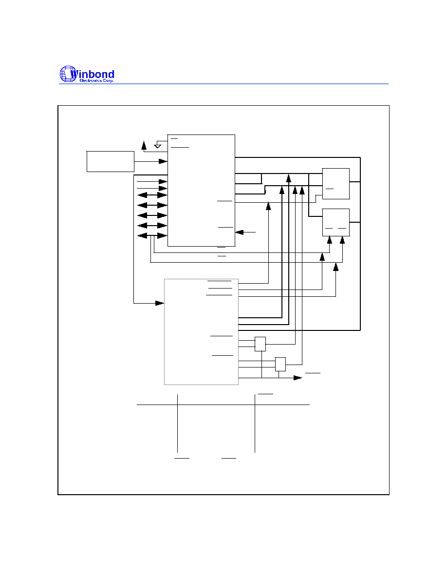
TYPICAL APPLICATION CIRCUITS
Advanced Type Application in Normal Mode
Note: ENSTD can also be left unconnected.
AP5<7:0>
AP6<7:0>
<7:0>
<15:8>
1MB
ROM
64KB
RAM
DP4<7:0>
P3<7:0>
P2<7:0>
P1<7:0>
P0<7:0>
OE
OE
WR
EA
ENSTD
VCC
PSEN
ADDR<15:0>
DB<7:0>
<7> (RD)
<6> (WR)
AP7<3:0>
ADDR<19:16>
P8<7:0>
INT3
INT2

W78958B
Publication Release Date: September 1997
- 25 -
Revision A3
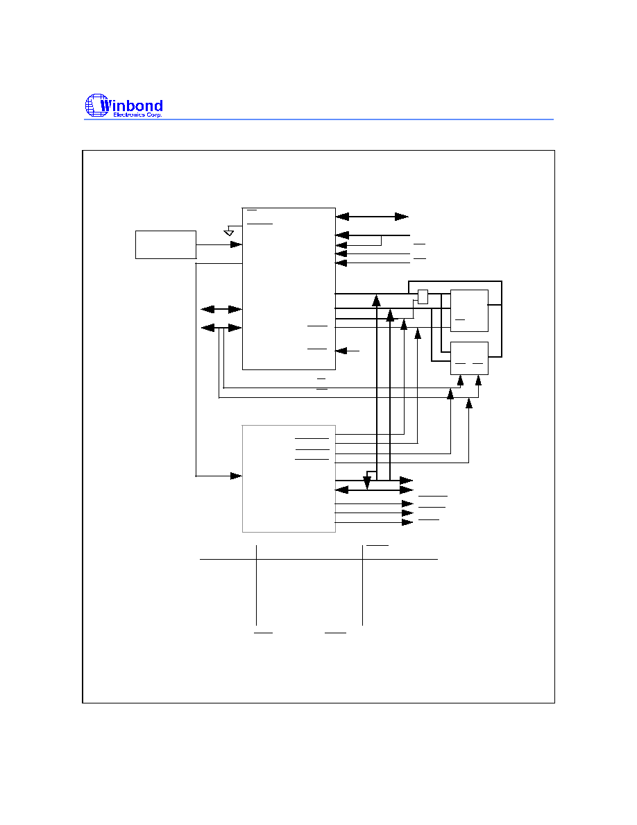
Standard Type Application in Normal Mode
Note: EA may be pulled high or low depending on application.
P3<7:0>
P1<7:0>
EA
ENSTD
<7> (RD)
<6> (WR)
AP5<7:0>
AP6<6:0>
DP4<7:0>
32KB
EPROM
depends on EA
P2<7:0>
P0<7:0>
64KB
RAM
OE
WR
<7:0>
<15:8>
ALE
64KB
ROM
OE
PSEN
74373
ROMS1
ROMS0
Vcc
(Example shown is W78C58.)
W78958B
- 26 -
Advanced Type Application in Emulation Mode
AP5<7:0>
AP6<7:0>
<7:0>
<15:8>
1MB
ROM
64KB
RAM
DP4<7:0>
P3<7:0>
P2<7:0>
P1<7:0>
P0<7:0>
EMU_ADDR<15:0>
EMU_DB<7:0>
OE
OE
WR
ICESET
EMU
ESEL
EA
ENSTD
VCC
ICE_CONTROL_LOGIC
ICE_BREAKPOINT
_LOGIC
PSEN
<7> (RD)
<6> (WR)
ROM_RD
RAM_RD
RAM_WR
INT_WR
INT_RD
EMU_ADDR<16>
EMU_ADDR<17>
SEL1
0
1
0
1
AP7<3:0>
<19:16>
EMU_ADDR<19:18>
P8<7:0>
INT3
INT2
ESEL
SEL1
SEL0
0
0
Internal RAM
0
1
SFR/PC
1
0
ROM
1
1
RAM
0 - FF
80 - FF
0 - FFFFF
0 - FFFF
ESEL
0
0
1
1
AP6<0>
0
1
-
-
access space
Note: When ESEL=1, ALE and PSEN are high-impedence.
W78958B
Publication Release Date: September 1997
- 27 -
Revision A3
Standard Type Application in Emulation Mode
P3<7:0>
P1<7:0>
EMU_ADDR<15:0>
EMU_DB<7:0>
ICESET
EMU
<7> (RD)
<6> (WR)
SEL1
ICE_CONTROL_LOGIC
ROM_RD
RAM_WR
EA
ENSTD
P2<7:0>
P0<7:0>
64KB
RAM
OE
WR
<7:0>
<15:8>
ALE
64KB
ROM
OE
PSEN
AP5<7:0>
AP6<0>
<7:0>
DP4<7:0>
ESEL
EMU_ALE
ICE_BREAKPOINT
_LOGIC
EMU_DB<7:0>
EMU_ADDR<8:0>
<8>
AP7<0>
AP7<1>
INT_WR
INT_RD
RAM_RD
INT_WR
INT_RD
ESEL
Note: When ESEL = 1, ALE and PSEN are high-impedence.
SEL1
SEL0
0
0
Internal RAM
0
1
SFR/PC
1
0
ROM
1
1
RAM
0 - FF
80 - FF
0 - FFFFF
0 - FFFF
ESEL
0
0
1
1
AP6<0>
0
1
-
-
Access Space
W78958B
- 28 -
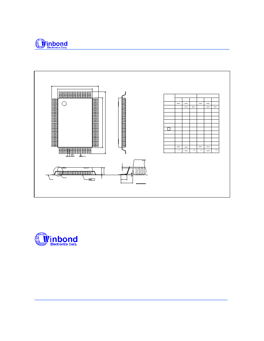
PACKAGE DIMENSIONS
100-pin QFP
51
50
31
30
1
80
81
100
1
A
H
D
D
e
b
E H
E
y
A
A
Seating Plane
L
L
1
See Detail F
Detail F
c
1. Dimension D & E do not include interlead
flash.
2. Dimension b does not include dambar
protrusion/intrusion.
3. Controlling dimension: Millimeters
4. General appearance spec. should be based
on final visual inspection spec.
0.102
0
12
0
0.004
2.413
1.397
19.10
1.194
18.80
0.991
18.49
0.095
0.055
0.988
0.752
0.047
0.976
0.740
0.039
0.964
0.728
0.65
20.13
14.13
0.254
0.407
2.972
3.30
20.00
14.00
2.845
19.87
13.87
0.101
0.254
2.718
0.10
0.792
0.556
0.010
0.016
0.117
0.130
0.787
0.551
0.112
0.026
0.782
0.546
0.004
0.010
0.107
0.004
Notes:
Symbol
Min.
Nom.
Max.
Max.
Nom.
Min.
Dimension in inches
Dimension in mm
A
b
c
D
e
H
D
H
E
L
y
A
A
L
1
1
2
E
0.012
0.006
0.152
0.305
24.49
24.80
25.10
12
0.020
0.087
0.032
0.103
0.498
0.802
2.21
2.616
2
Headquarters
No. 4, Creation Rd. III,
Science-Based Industrial Park,
Hsinchu, Taiwan
TEL: 886-3-5770066
FAX: 886-3-5792697
http://www.winbond.com.tw/
Voice & Fax-on-demand: 886-2-7197006
Taipei Office
11F, No. 115, Sec. 3, Min-Sheng East Rd.,
Taipei, Taiwan
TEL: 886-2-7190505
FAX: 886-2-7197502
Winbond Electronics (H.K.) Ltd.
Rm. 803, World Trade Square, Tower II,
123 Hoi Bun Rd., Kwun Tong,
Kowloon, Hong Kong
TEL: 852-27513100
FAX: 852-27552064
Winbond Electronics North America Corp.
Winbond Memory Lab.
Winbond Microelectronics Corp.
Winbond Systems Lab.
2727 N. First Street, San Jose,
CA 95134, U.S.A.
TEL: 408-9436666
FAX: 408-5441798
Note: All data and specifications are subject to change without notice.