
Preliminary W78C52D
8-BIT MICROCONTROLLER
Publication Release Date: December 1998
- 1 -
Revision A1
GENERAL DESCRIPTION
The W78C52D microcontroller supplies a wider frequency and supply voltage range than most 8-bit
microcontrollers on the market. It is compatible with the industry standard 80C52 microcontroller
series. The W78C52D contains four 8-bit bidirectional parallel ports, one extra 4-bit bit-addressable
I/O port (Port 4) and two additional external interrupts (
INT2
, INT3 ), three 16-bit timer/counters, one
watchdog timer and a serial port. These peripherals are supported by a eight-source, two-level
interrupt capability. There are 256 bytes of RAM and an 8K byte mask ROM for application programs.
The W78C52D microcontroller has two power reduction modes, idle mode and power-down mode,
both of which are software selectable. The idle mode turns off the processor clock but allows for
continued peripheral operation. The power-down mode stops the crystal oscillator for minimum power
consumption. The external clock can be stopped at any time and in any state without affecting the
processor.
FEATURES
∑
Fully static design
∑
Supply voltage of 4.5V to 5.5V
∑
DC-40 MHz operation
∑
256 bytes of on-chip scratchpad RAM
∑
8K bytes of on-chip mask ROM
∑
64K bytes program memory address space
∑
64K bytes data memory address space
∑
Four 8-bit bidirectional ports
∑
Three 16-bit timer/counters
∑
One full duplex serial port
∑
Eight
-source, two-level interrupt capability
∑
One extra 4-bit bit-addressable I/O port
∑
Two additional external interrupts
INT2
/ INT3
∑
Watchdog timer
∑
EMI reduction mode
∑
Built-in power management
∑
Code protection
∑
Packages:
-
DIP 40: W78C52D-24/40
-
PLCC 44: W78C52DP-24/40
-
QFP 44: W78C52DF-24/40
Preliminary W78C52D
- 2 -
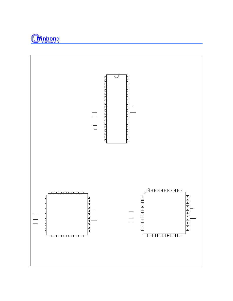
PIN CONFIGURATIONS
VDD
1
2
3
4
5
6
7
8
9
10
11
12
13
14
15
16
17
18
19
20
39
40
34
35
36
37
38
30
31
32
33
26
27
28
29
21
22
23
24
25
P0.0, AD0
P0.1, AD1
P0.2, AD2
P0.3, AD3
P0.4, AD4
P0.5, AD5
P0.6, AD6
P0.7, AD7
EA
ALE
PSEN
P2.5, A13
P2.6, A14
P2.7, A15
P2.0, A8
P2.1, A9
P2.2, A10
P2.3, A11
P2.4, A12
T2, P1.0
40-Pin DIP (W78C52D)
P1.2
P1.3
P1.4
P1.5
P1.6
RXD, P3.0
TXD, P3.1
P1.7
RST
INT0, P3.2
INT1, P3.3
T0, P3.4
T1, P3.5
WR, P3.6
RD, P3.7
XTAL1
XTAL2
VSS
T2EX, P1.1
44-Pin PLCC (W78C52DP)
44-Pin QFP (W78C52DF)
40
2 1 44 43 42 41
6 5 4 3
39
38
37
36
35
34
33
32
31
30
29
28
27
26
25
24
23
22
21
20
19
18
17
10
9
8
7
14
13
12
11
16
15
P1.5
P1.6
P1.7
RST
RXD, P3.0
TXD, P3.1
INT0, P3.2
INT1, P3.3
T0, P3.4
T1, P3.5
A
D
3
,
P
0
.
3
T
2
,
P
1
.
0
P
1
.
2
V
D
D
A
D
2
,
P
0
.
2
A
D
1
,
P
0
.
1
A
D
0
,
P
0
.
0
T
2
E
X
,
P
1
.
1
P
1
.
3
P
1
.
4
X
T
A
L
1
V
S
S
P
2
.
4
,
A
1
2
P
2
.
3
,
A
1
1
P
2
.
2
,
A
1
0
P
2
.
1
,
A
9
P
2
.
0
,
A
8
X
T
A
L
2
P
3
.
7
,
/
R
D
P
3
.
6
,
/
W
R
P0.4, AD4
P0.5, AD5
P0.6, AD6
P0.7, AD7
EA
ALE
PSEN
P2.7, A15
P2.6, A14
P2.5, A13
P4.1
P
4
.
0
INT2, P4.3
/
I
N
T
3
,
P
4
.
2
34
40 39 38 37 36 35
44 43 42 41
33
32
31
30
29
28
27
26
25
24
23
P0.4, AD4
P0.5, AD5
P0.6, AD6
P0.7, AD7
EA
ALE
PSEN
P2.7, A15
P2.6, A14
P2.5, A13
22
21
20
19
18
17
16
15
14
13
12
11
4
3
2
1
8
7
6
5
10
9
P1.5
P1.6
P1.7
RST
RXD, P3.0
TXD, P3.1
INT0, P3.2
INT1, P3.3
T0, P3.4
T1, P3.5
X
T
A
L
1
V
S
S
P
2
.
4
,
A
1
2
P
2
.
3
,
A
1
1
P
2
.
2
,
A
1
0
P
2
.
1
,
A
9
P
2
.
0
,
A
8
X
T
A
L
2
P
3
.
7
,
/
R
D
P
3
.
6
,
/
W
R
A
D
3
,
P
0
.
3
T
2
,
P
1
.
0
P
1
.
2
V
D
D
A
D
2
,
P
0
.
2
A
D
1
,
P
0
.
1
A
D
0
,
P
0
.
0
T
2
E
X
,
P
1
.
1
P
1
.
3
P
1
.
4
P
4
.
0
/
I
N
T
3
,
P
4
.
2
P4.1
INT2, P4.3
Preliminary W78C52D
Publication Release Date: December 1998
- 3 -
Revision A1
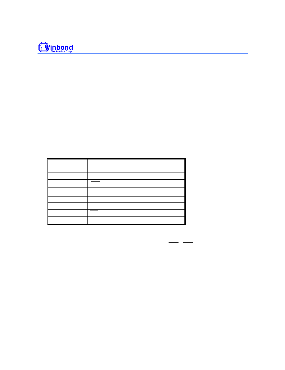
PIN DESCRIPTION
P0.0
-
P0.7
Port 0, Bits 0 through 7. Port 0 is a bidirectional I/O port. This port also provides a multiplexed low
order address/data bus during accesses to external memory.
P1.0
-
P1.7
Port 1, Bits 0 through 7. Port 1 is a bidirectional I/O port with internal pull-ups. Pins P1.0 and P1.1
also serve as T2 (Timer 2 external input) and T2EX (Timer 2 capture/reload trigger), respectively.
P2.0
-
P2.7
Port 2, Bits 0 through 7. Port 2 is a bidirectional I/O port with internal pull-ups. This port also provides
the upper address bits for accesses to external memory.
P3.0
-
P3.7
Port 3, Bits 0 through 7. Port 3 is a bidirectional I/O port with internal pull-ups. All bits have alternate
functions, which are described below:
PIN
ALTERNATE FUNCTION
P3.0
RXD Serial Receive Data
P3.1
TXD Serial Transmit Data
P3.2
INT0 External Interrupt 0
P3.3
INT1 External Interrupt 1
P3.4
T0 Timer 0 Input
P3.5
T1 Timer 1 Input
P3.6
WR Data Write Strobe
P3.7
RD Data Read Strobe
P4.0
-
P4.3
Another bit-addressable bidirectional I/O port P4. P4.3 and P4.2 are alternative function pins. It can
be used as general I/O pins or external interrupt input sources (
INT2
/ INT3 ).
EA
External Address Input, active low. This pin forces the processor to execute out of external ROM.
This pin should be kept low for all W78C31 operations.
RST
Reset Input, active high. This pin resets the processor. It must be kept high for at least two machine
cycles in order to be recognized by the processor.
ALE
Address Latch Enable Output, active high. ALE is used to enable the address latch that separates the
address from the data on Port 0. ALE runs at 1/6th of the oscillator frequency. A single ALE pulse is
skipped during external data memory accesses. ALE goes to a high impedance state during reset with
a weak pull-up.
Preliminary W78C52D
- 4 -
PSEN
Program Store Enable Output, active low.
PSEN
enables the external ROM onto the Port 0
address/data bus during fetch and MOVC operations.
PSEN
goes to a high impedance state during
reset with a weak pull-up.
XTAL1
Crystal 1. This is the crystal oscillator input. This pin may be driven by an external clock.
XTAL2
Crystal 2. This is the crystal oscillator output. It is the inversion of XTAL1.
V
SS
, V
DD
Power Supplies. These are the chip ground and positive supplies.
BLOCK DIAGRAM
P3.0
~
P3.7
P1.0
~
P1.7
ALU
Port 0
Latch
Port 1
Latch
Timer
1
Timer
0
Timer
2
Port
1
UART
XTAL1
PSEN
ALE
GND
VDD
RST
XTAL2
Oscillator
Interrupt
PSW
Instruction
Decoder
&
Sequencer
Reset Block
Bus & Clock
Controller
SFR RAM
Address
Power control
256 bytes
RAM & SFR
Stack
Pointer
B
Addr. Reg.
Incrementor
PC
DPTR
Temp Reg.
T2
T1
ACC
Port 3
Latch
Port 4
Latch
Port
3
Port 2
Latch
P4.0
~
P4.3
Port
4
Port
0
Port
2
P2.0
~
P2.7
P0.0
~
P0.7
INT2
INT3
Watchdog
Timer
8K bytes
ROM

Preliminary W78C52D
Publication Release Date: December 1998
- 5 -
Revision A1
FUNCTIONAL DESCRIPTION
The W78C52D architecture consists of a core controller surrounded by various registers, five general
purpose I/O ports, 256 bytes of RAM, three timer/counters, one watchdog timer and a serial port. The
processor supports 111 different opcodes and references both a 64K program address space and a
64 K data storage space.
Timers 0, 1, and 2
Timers 0, 1, and 2 each consist of two 8-bit data registers. These are called TL0 and TH0 for Timer
0, TL1 and TH1 for Timer 1, and TL2 and TH2 for Timer 2. The TCON and TMOD registers provide
control functions for timers 0, 1. The T2CON register provides control functions for Timer 2. RCAP2H
and RCAP2L are used as reload/capture registers for Timer 2. The operations of Timer 0 and Timer
1 are the same as in the W78C51. Timer 2 is a special feature of the W78C52D: it is a 16-bit
timer/counter that is configured and controlled by the T2CON register. Like Timers 0 and 1, Timer 2
can operate as either an external event counter or as an internal timer, depending on the setting of
bit C/T2 in T2CON. Timer 2 has three operating modes: capture, auto-reload, and baud rate
generator. The clock speed at capture or auto-reload mode is the same as that of Timers 0 and 1.
Clock
The W78C52D is designed to be used with either a crystal oscillator or an external clock. Internally,
the clock is divided by two before it is used. This makes the W78C52D relatively insensitive to duty
cycle variations in the clock.
Crystal Oscillator
The W78C52D incorporates a built-in crystal oscillator. To make the oscillator work, a crystal must be
connected across pins XTAL1 and XTAL2. In addition, a load capacitor must be connected from each
pin to ground, and a resistor must also be connected from XTAL1 to XTAL2 to provide a DC bias
when the crystal frequency is above 24 MHz.
External Clock
An external clock should be connected to pin XTAL1. Pin XTAL2 should be left unconnected. The
XTAL1 input is a CMOS-type input, as required by the crystal oscillator. As a result, the external clock
signal should have an input one level of greater than 3.5 volts when V
DD
= 5 volts.
Power Management
Idle Mode
The idle mode is entered by setting the IDL bit in the PCON register. In the idle mode, the internal
clock to the processor is stopped. The peripherals and the interrupt logic continue to be clocked. The
processor will exit idle mode when either an interrupt or a reset occurs.
Power-down Mode
When the PD bit of the PCON register is set, the processor enters the power-down mode. In this
mode all of the clocks, including the oscillator are stopped. The only way to exit power-down mode is
by a reset.
Reset
The external RESET signal is sampled at S5P2. To take effect, it must be held high for at least two
machine cycles while the oscillator is running. An internal trigger circuit in the reset line is used to