 | –≠–ª–µ–∫—Ç—Ä–æ–Ω–Ω—ã–π –∫–æ–º–ø–æ–Ω–µ–Ω—Ç: W78E58BP | –°–∫–∞—á–∞—Ç—å:  PDF PDF  ZIP ZIP |

W78E58B
8-BIT MICROCONTROLLER
Publication Release Date: March 18, 2002
- 1 - Revision A3
1. GENERAL DESCRIPTION
The W78E58B is an 8-bit microcontroller which has an in-system programmable Flash EPROM for
firmware updating. The instruction set of the W78E58B is fully compatible with the standard 8052. The
W78E58B contains a 32K bytes of main ROM and a 4K bytes of auxiliary ROM which allows the
contents of the 32KB main ROM to be updated by the loader program located at the 4KB auxiliary
ROM; 512 bytes of on-chip RAM; four 8-bit bi-directional and bit-addressable I/O ports; an additional 4-
bit port P4; three 16-bit timer/counters; a serial port. These peripherals are supported by a eight
sources two-level interrupt capability. To facilitate programming and verification, the ROM inside the
W78E58B allows the program memory to be programmed and read electronically. Once the code is
confirmed, the user can protect the code for security.
The W78E58B microcontroller has two power reduction modes, idle mode and power-down mode,
both of which are software selectable. The idle mode turns off the processor clock but allows for
continued peripheral operation. The power-down mode stops the crystal oscillator for minimum power
consumption. The external clock can be stopped at any time and in any state without affecting the
processor.
2. FEATURES
∑
Fully static design 8-bit CMOS microcontroller
∑
32K bytes of in-system programmable Flash EPROM for Application Program (APROM)
∑
4K bytes of auxiliary ROM for Loader Program (LDROM)
∑
512 bytes of on-chip RAM (including 256 bytes of AUX-RAM, software selectable)
∑
64K bytes program memory address space and 64K bytes data memory address space
∑
Four 8-bit bi-directional ports
∑
One 4-bit multipurpose programmable port
∑
Three 16-bit timer/counters
∑
One full duplex serial port
∑
Eight-sources, two-level interrupt capability
∑
Built-in power management
∑
Code protection
∑
Packaged in
-
DIP 40: W78E58B-24/40
-
PLCC 44: W78E58BP-24/40
-
QFP 44: W78E58BF-24/40
W78E58B
- 2 -
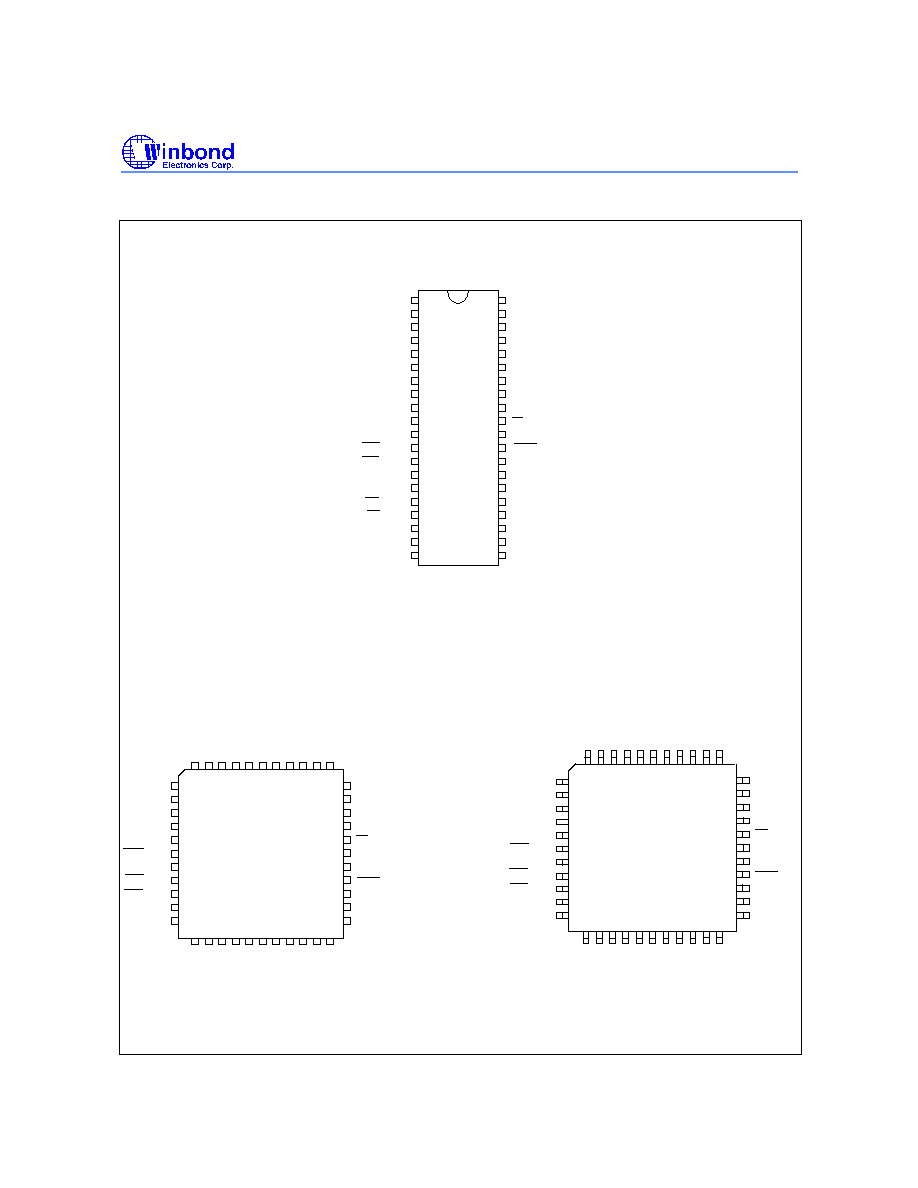
3. PIN CONFIGURATIONS
VDD
1
2
3
4
5
6
7
8
9
10
11
12
13
14
15
16
17
18
19
20
39
40
34
35
36
37
38
30
31
32
33
26
27
28
29
21
22
23
24
25
P0.0, AD0
P0.1, AD1
P0.2, AD2
P0.3, AD3
P0.4, AD4
P0.5, AD5
P0.6, AD6
P0.7, AD7
EA
ALE
PSEN
P2.5, A13
P2.6, A14
P2.7, A15
P2.0, A8
P2.1, A9
P2.2, A10
P2.3, A11
P2.4, A12
T2, P1.0
40-Pin DIP (W78E58B)
P1.2
P1.3
P1.4
P1.5
P1.6
RXD, P3.0
TXD, P3.1
P1.7
RST
INT0, P3.2
INT1, P3.3
T0, P3.4
T1, P3.5
W R , P3.6
RD, P3.7
XTAL1
XTAL2
VSS
T2EX, P1.1
44-Pin PLCC (W78E58BP)
44-Pin QFP (W78E58BF)
40
2
1 44 43 42 41
6
5
4
3
39
38
37
36
35
34
33
32
31
30
29
28
27
26
25
24
23
22
21
20
19
18
17
10
9
8
7
14
13
12
11
16
15
P1.5
P1.6
P1.7
RST
RXD, P3.0
TXD, P3.1
INT0, P3.2
INT1, P3.3
T0, P3.4
T1, P3.5
A
D
3
,
P
0
.
3
T
2
,
P
1
.
0
P
1
.
2
V
D
D
A
D
2
,
P
0
.
2
A
D
1
,
P
0
.
1
A
D
0
,
P
0
.
0
T
2
E
X
,
P
1
.
1
P
1
.
3
P
1
.
4
X
T
A
L
1
V
S
S
P
2
.
4
,
A
1
2
P
2
.
3
,
A
1
1
P
2
.
2
,
A
1
0
P
2
.
1
,
A
9
P
2
.
0
,
A
8
X
T
A
L
2
P
3
.
7
,
/
R
D
P
3
.
6
,
/
W
R
P0.4, AD4
P0.5, AD5
P0.6, AD6
P0.7, AD7
EA
ALE
PSEN
P2.7, A15
P2.6, A14
P2.5, A13
P4.1
P
4
.
0
INT2, P4.3
/
I
N
T
3
,
P
4
.
2
34
40 39 38 37 36 35
44 43 42 41
33
32
31
30
29
28
27
26
25
24
23
P0.4, AD4
P0.5, AD5
P0.6, AD6
P0.7, AD7
EA
ALE
PSEN
P2.7, A15
P2.6, A14
P2.5, A13
22
21
20
19
18
17
16
15
14
13
12
11
4
3
2
1
8
7
6
5
10
9
P1.5
P1.6
P1.7
RST
RXD, P3.0
TXD, P3.1
INT0, P3.2
INT1, P3.3
T0, P3.4
T1, P3.5
X
T
A
L
1
V
S
S
P
2
.
4
,
A
1
2
P
2
.
3
,
A
1
1
P
2
.
2
,
A
1
0
P
2
.
1
,
A
9
P
2
.
0
,
A
8
X
T
A
L
2
P
3
.
7
,
/
R
D
P
3
.
6
,
/
W
R
A
D
3
,
P
0
.
3
T
2
,
P
1
.
0
P
1
.
2
V
D
D
A
D
2
,
P
0
.
2
A
D
1
,
P
0
.
1
A
D
0
,
P
0
.
0
T
2
E
X
,
P
1
.
1
P
1
.
3
P
1
.
4
P
4
.
0
/
I
N
T
3
,
P
4
.
2
P4.1
INT2, P4.3
W78E58B
Publication Release Date: March 18, 2002
- 3 - Revision A3
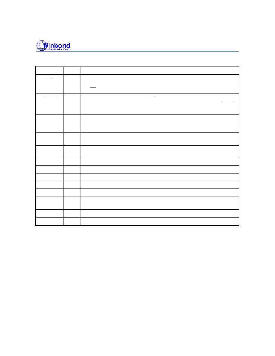
4. PIN DESCRIPTION
SYMBOL TYPE
DESCRIPTIONS
EA
I
EXTERNAL ACCESS ENABLE: This pin forces the processor to execute the
external ROM. The ROM address and data will not be presented on the bus if
the EA pin is high.
PSEN
O H PROGRAM STORE ENABLE: PSEN enables the external ROM data in the
Port 0 address/data bus. When internal ROM access is performed, no PSEN
strobe signal outputs originate from this pin.
ALE
O H ADDRESS LATCH ENABLE: ALE is used to enable the address latch that
separates the address from the data on Port 0. ALE runs at 1/6th of the
oscillator frequency.
RST
I L RESET: A high on this pin for two machine cycles while the oscillator is running
resets the device.
XTAL1
I
CRYSTAL 1: This is the crystal oscillator input. This pin may be driven by an
external clock.
XTAL2
O CRYSTAL 2: This is the crystal oscillator output. It is the inversion of XTAL1.
V
SS
I
GROUND: Ground potential.
V
DD
I
POWER SUPPLY: Supply voltage for operation.
P0.0
-
P0.7 I/O D PORT 0: Function is the same as that of standard 8052.
P1.0
-
P1.7 I/O H PORT 1: Function is the same as that of standard 8052.
P2.0
-
P2.7 I/O H PORT 2: Port 2 is a bi-directional I/O port with internal pull-ups. This port also
provides the upper address bits for accesses to external memory.
P3.0
-
P3.7 I/O H PORT 3: Function is the same as that of the standard 8052.
P4.0
-
P4.3 I/O H PORT 4: A bi-directional I/O. See details below.
* Note: TYPE I: input, O: output, I/O: bi-directional, H: pull-high, L: pull-low, D: open drain
W78E58B
- 4 -
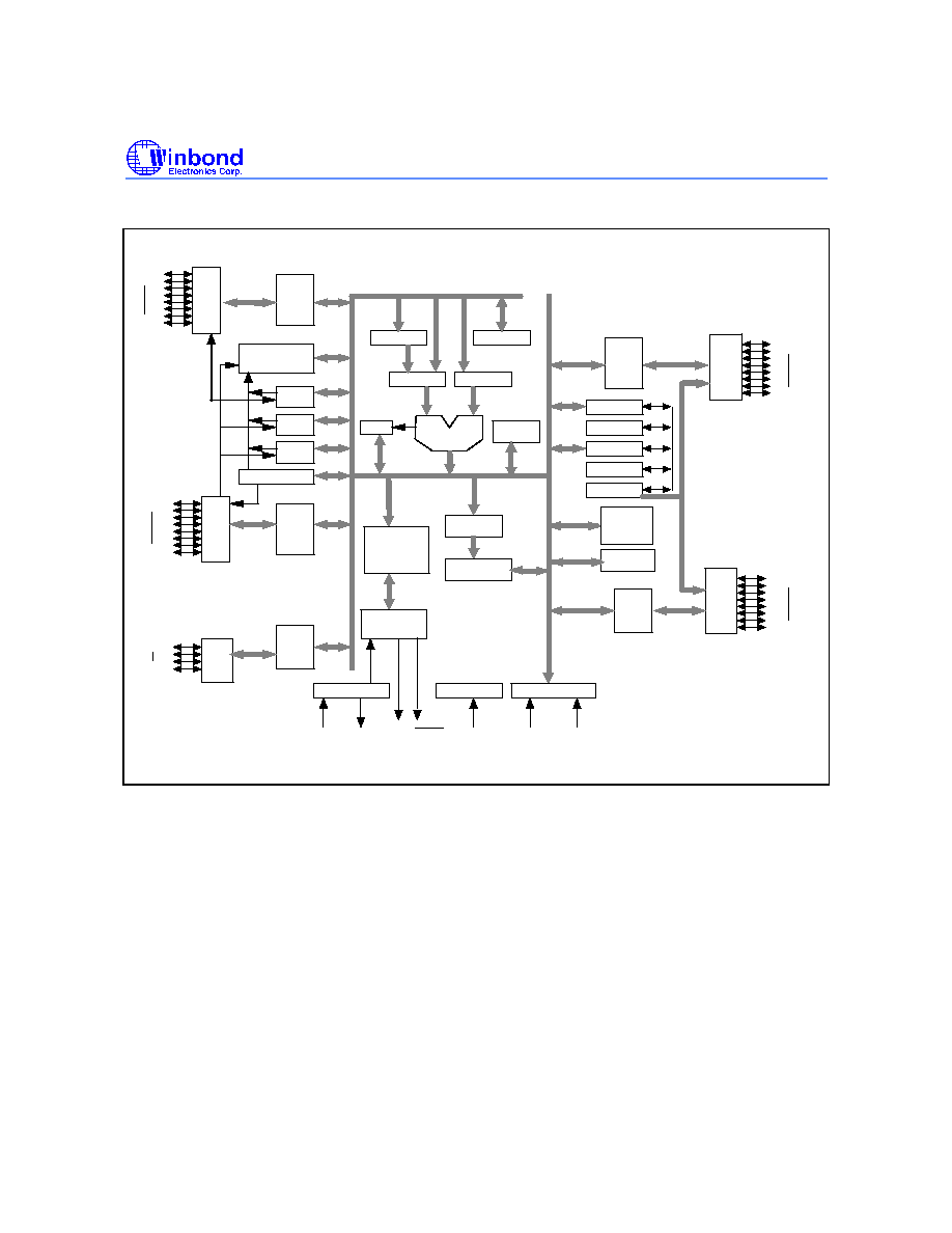
5. BLOCK DIAGRAM
P3.0
P3.7
P1.0
P1.7
ALU
Port 0
Latch
Port 1
Latch
Timer
1
Timer
0
Timer
2
Port
1
UART
XTAL1
PSEN
ALE
Vss
VCC
RST
XTAL2
Oscillator
Interrupt
PSW
Instruction
Decoder
&
Sequencer
Reset Block
Bus & Clock
Controller
SFR RAM
Address
Power control
512 bytes
RAM & SFR
Stack
Pointer
B
Addr. Reg.
Incrementor
PC
DPTR
Temp Reg.
T2
T1
ACC
Port 3
Latch
Port 4
Latch
Port
3
Port 2
Latch
P4.0
P4.3
Port
4
Port
0
Port
2
P2.0
P2.7
P0.0
P0.7
32KB
ROM
4KB
ROM
6. FUNCTIONAL DESCRIPTION
The W78E58B architecture consists of a core controller surrounded by various registers, four general
purpose I/O ports, one special purpose programmable 4-bits I/O port, 512 bytes of RAM, three
timer/counters, a serial port. The processor supports 111 different opcodes and references both a 64K
program address space and a 64K data storage space.
RAM
The internal data RAM in the W78E58B is 512 bytes. It is divided into two banks: 256 bytes of
scratchpad RAM and 256 bytes of AUX-RAM. These RAMs are addressed by different ways.
∑
RAM 0H
-
7FH can be addressed directly and indirectly as the same as in 8051. Address pointers
are R0 and R1 of the selected register bank.
∑
RAM 80H
-
FFH can only be addressed indirectly as the same as in 8051. Address pointers are R0,
R1 of the selected registers bank.

W78E58B
Publication Release Date: March 18, 2002
- 5 - Revision A3
∑
AUX-RAM 0H
-
FFH is addressed indirectly as the same way to access external data memory with
the MOVX instruction. Address pointer are R0 and R1 of the selected register bank and DPTR
register. An access to external data memory locations higher than FFH will be performed with the
MOVX instruction in the same way as in the 8051. The AUX-RAM is disable after a reset. Setting
the bit 4 in CHPCON register will enable the access to AUX-RAM. When AUX-RAM is enabled the
instructions of "MOVX @Ri" will always access to on-chip AUX-RAM. When executing from internal
program memory, an access to AUX-RAM will not affect the Ports P0, P2, WR and RD .
Example,
CHPENR REG F6H
CHPCON REG BFH
MOV CHPENR, #87H
MOV CHPENR, #59H
ORL CHPCON, #00010000B ; enable AUX-RAM
MOV CHPENR, #00H
MOV R0, #12H
MOV A, #34H
MOVX @R0, A ; Write 34h data to 12h address.
Timers 0, 1 and 2
Timers 0, 1, and 2 each consist of two 8-bit data registers. These are called TL0 and TH0 for Timer 0,
TL1 and TH1 for Timer 1, and TL2 and TH2 for Timer 2. The TCON and TMOD registers provide
control functions for timers 0, 1. The T2CON register provides control functions for Timer 2. RCAP2H
and RCAP2L are used as reload/capture registers for Timer 2. The operations of Timer 0 and Timer 1
are the same as in the W78C51. Timer 2 is a 16-bit timer/counter that is configured and controlled by
the T2CON register. Like Timers 0 and 1, Timer 2 can operate as either an external event counter or
as an internal timer, depending on the setting of bit C/T2 in T2CON. Timer 2 has three operating
modes: capture, auto-reload, and baud rate generator. The clock speed at capture or auto-reload
mode is the same as that of Timers 0 and 1.
Clock
The W78E58B is designed with either a crystal oscillator or an external clock. Internally, the clock is
divided by two before it is used by default. This makes the W78E58B relatively insensitive to duty cycle
variations in the clock.
Crystal Oscillator
The W78E58B incorporates a built-in crystal oscillator. To make the oscillator work, a crystal must be
connected across pins XTAL1 and XTAL2. In addition, a load capacitor must be connected from each
pin to ground.
External Clock
An external clock should be connected to pin XTAL1. Pin XTAL2 should be left unconnected. The
XTAL1 input is a CMOS-type input, as required by the crystal oscillator.