
W81
2
82F
USB Keyboard Controller
with
4 Ports Hub

W81282F Data Sheet Revision History
Pages
Dates
Version Version
on Web
Main Contents
1
n.a.
08/27/99
0.50
n.a.
First published.
2
3
4
5
6
7
8
9
10
Please note that all data and specifications are subject to change without notice. All
the trade marks of products and companies mentioned in this data sheet belong to
their respective owners.
LIFE SUPPORT APPLICATIONS
These products are not designed for use in life support appliances, devices, or
systems where malfunction of these products can reasonably be expected to result
in personal injury. Winbond customers using or selling these products for use in such
applications do so at their own risk and agree to fully indemnify Winbond for any
damages resulting from such improper use or sales.

W81282F
Preliminary
Publication Release Date: Aug. 199
9
- 1 -
Revision 0.5
TABLE OF CONTENTS
1. GENERAL DESCRIPTION
.................................................................................................................1
2.
APPLICATION BLOCK DIAGRAM
....................................................................................................1
3. FEATURES ............................................................................................................................................2
4. PIN CONFIGURATION
.......................................................................................................................3
5. PIN DESCRIPTION
.............................................................................................................................4
6. ABSOLUTE MAXIMUM RATINGS
....................................................................................................8
7. ELECTRICAL CHARACTERISTICS
..................................................................................................9
8. TYPICAL APPLICATION
.................................................................................................................. 11
9. HOW TO READ THE TOP MARKING
............................................................................................. 13
10. PACKAGE DIMENSIONS
............................................................................................................... 14

W81282F
USB HUB CONTROLLER
Publication Release Date: Aug. 199
9
- 1 -
Revision 0.71
1. GENERAL DESCRIPTION
The W81282F is a highly integrated USB keyboard with 4 port hub controller chip. The W81282F has a
built-in 21X8 default keyboard matrix, so that it can be directly connected to keyboard with multi-media
function matrix. The keyboard matrix, vendor ID, and device ID can be easily customized from an
optional EEPROM or modify firmware to meet any customers' requirement. The 4 USB down-stream
port can be used to connect various USB peripheral devices, such as printer, modem, speaker,
camera, mice, and joystick, to system without any external glue logics. The W81282F use 12MHz
clock input with internal PLL to eliminate EMI effect. The W81282F also built-in ESD/EFT protection
circuit so it can pass ESD/EFT test without any external glue logics.
2.
APPLICATION BLOCK DIAGRAM
KB MATRIX
HOST
4 PORT USB DOWNLINK
W81282F
EEPROM
(Optional)
ID, Matrix Loadable
Volume Control
KB MATRIX
KB MATRIX
HOST
4 PORT USB DOWNLINK
W81282F
EEPROM
(Optional)
ID, Matrix Loadable
Volume Control

W81282F
PRELIMINARY
Publication Release Date: Aug. 199
9
- 2 -
Revision 0.5
3. FEATURES
�
Full compliance with USB spec Rev 1.
1
and HID Class Definition Rev 1.0
�
Embedded microprocessor--8052 ( 6K ROM + 256 Byte RAM)
�
Support auto-detected two power source mode between bus power mode and self power mode.
�
12-Mhz crystal/oscillator input to lower EMI
�
Support Suspend and Resume operation
�
Support ACPI features
�
Four downstream ports with per port over-current protection
�
Single 5V supplied with embedded 5V-3.3V regulator
�
Provides the external pull-up resistor control for the up-stream connection.
�
Per-port/Global power control optional
�
Built-in ESD/EFT protection circuit
�
Support 21 X 8 keyboard matrix
�
Support consumer control function for multi-media
�
Support optional EEPROM for vendor ID, device ID, and KB matrix down load
�
Support encoder input for audio volume control
�
Provide the external pull-up resistor control for the up-stream connect
�
100-pin PQFP
�
5V CMOS device
W81282F
PRELIMINARY
Publication Release Date: Aug. 199
9
- 3 -
Revision 0.5
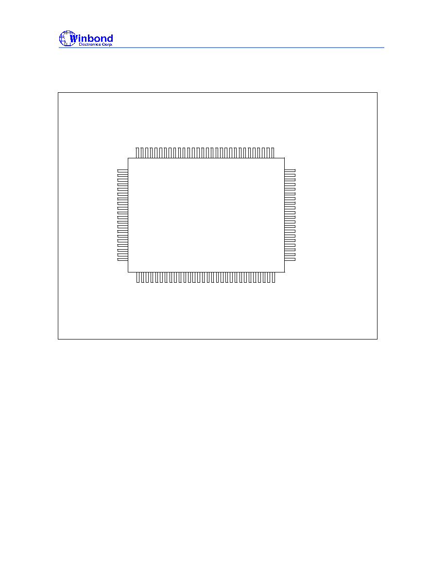
4. PIN CONFIGURATION
XRD#(P37)
D P 4
D M 4
D P 3
D M 3
G N D 3 V
G N D 3 V
D P 2
D M 2
D P 1
D M 1
G N D 3 V
G N D 3 V
D P 0
D M 0
50
49
48
47
46
45
44
43
42
41
40
39
38
37
36
35
34
33
32
31
81
82
83
84
85
86
87
88
89
90
91
92
93
94
95
96
97
98
99
100
O V R I 4 #
SO03(P04)
S O 1 8
SO02(P05)
SO01(P06)
V D D
SO00(P07)
N .C.
X T A L 2
X T A L 1
G N D
N .C.
N .C.
L E D E N 1 #
PLLE
L E D E N 2 #
R B
L E D E N 3 #
RA
LEDEN4#
1 2 3 4 5 6 7 8 9
1
0
1
1
1
2
1
3
1
4
1
5
1
6
1
7
1
8
1
9
2
0
2
1
2
2
2
3
2
4
2
5
2
6
2
7
2
8
2
9
3
0
7
1
7
0
6
9
6
8
6
7
6
6
6
5
6
4
6
3
6
2
6
1
6
0
5
9
5
8
5
7
5
6
5
5
5
4
5
3
5
2
5
1
7
2
7
3
7
4
7
5
7
6
7
7
7
8
7
9
8
0
EECLK/IDSEL0(P30)
SO04(P03)
UPWEN4#
OVRI3#
SO05(P02)
UPWEN3#
SO06(P01)
LEDEN0#
XWR#(P36)
SO07(P00)
OVRI2#
P35
UPWEN2#
GND3V
SO20(P34)
SO19
GND
GND
N.C.
SO08(P20)
OVRI1#
SO09(P21)
UPWEN1#
SO10(P22)
FWKP5#
SO11(P23)
SO12(P24))
SO13(P25)
GND3V
VDDA
SO14 (P26)
GNDA
VBUS
SO15(P27)
LED0#
SI0(P10)
LED1#
SI11(P11)
VDD
N.C.
LED2#
SI2(P12)
SI4(P14)
LEDOVR#
SI3(P13)
VDD
RESET
INPUT_P
SO16
P33
XINT# (P32)
EESDA/IDSEL1(P31)
SI5(P15)
SI6(P16)
BUSPWR#
SO17
GANGED#
SI7(P17)
VDD3V
N.C.
N.C.
N.C.
N.C.
N.C.
N.C.
W81282F

W81282F
PRELIMINARY
Publication Release Date: Aug. 199
9
- 4 -
Revision 0.5
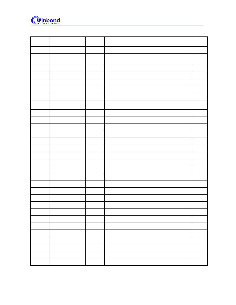
5. PIN DESCRIPTION
Pin
Number
Pin Name
I/O Type
Pin Function
Pull
Up/
Down
1
VDD3V
Power1
3.3V Regulator Output. Supplying voltage for all transceivers
-
2
VDDA
Power1
Analog power.
-
3
SO14 (P26)
IOUD2
Port 2.6 and function of Scan Out line 14.
U
4
GNDA
Power0
Analog ground.
-
5
VBUS
IUD2T
Input of upstream power status. On self-power mode, connection
should be controlled by VBUS status.
-
6
SO15 (P27)
IOUD2
Port 2.7 and function of Scan Out line 15.
U
7
LED0
#
IOU2P
Keyboard NumLock LED driver. To drive LED directly.
O
8
SI
0
(P10)
IOUD2
Port 1.
0
and function of Scan In line
0
.
U
9
LED1
#
IOU2P
Keyboard CapLock LED driver. To drive LED directly.
O
10
SI
1
(P11)
IOUD2
Port 1.
1
and function of Scan In line
1
.
U
11
LED2
#
IOU2P
Keboard ScrolLock LED driver. To drive LED directly
O
12
SI
2
(P12)
IOUD2
Port 1.
2
and function of Scan In line
2
.
U
13
LEDOVR#
IOU2P
Flag of
any downstream
port1 over-current. To drive LED directly
O
14
SI
3
(P13)
IOUD2
Port 1.
3
and function of Scan In line
3
.
U
15,16
VDD
Power1
Digital supply voltage.
-
17
SI
4
(P14)
IOUD2
Port 1.
4
and function of Scan In line
4
.
U
18
N.C.
IOUD2
No connection. This pin should be floated.
U
19
RESET
IUD2T
Master reset input. Active high.
-
20
INPUT_P
IOUD2
A programmable port and reverse for input application.
U
21
SO16
O2
This pin is function of Scan Out line 16.
-
22
P33
IOUD2
Port 3.3
and reverse for input or output application.
U
23
XINT# (P32)
IOUD2
Port 3.2
. This pin is dedicated for internal use.
U
24
EESDA
/IDSEL1
(P31)
IOUD2
Port 3.1 and function of
serial data line interfacing with external
EEPROM. If no serial EEPROM present, this pin is used to scan
ID selection and named IDSEL
1
U
25
SI
5
(P15)
IOUD2
Port 1.
5
and function of Scan In line
5
.
U
26
SI
6
(P1
6
)
IOUD2
Port 1.
6
and function of Scan In line
6
.
U
27
SI7 (P1
7
)
IOUD2
Port 1.
7
and function of Scan In line
7
.
U
W81282F
PRELIMINARY
Publication Release Date: Aug. 199
9
- 5 -
Revision 0.5
28
BUSPWR#
IUD2
Buspower/Selfpower control setting.
This pin should be floated or
tied to VDD.
D
29
SO1
7
IOU2P
This pin is function of Scan Out line 1
7
.
O
30
GANGED
#
IUD2
Ganged/Individual downstream power switch control setting.
Default is Individual mode.
U
31
LEDEN4#
IOU2P
Downstream port4 LED. Active low when port4 enable.
O
32
RA
IUD2
This pin is a Rotation A input for consumer HID application.
U
33
LEDEN3#
IOU2P
Downstream port3 LED. Active low when port3 enable.
O
34
RB
IUD2
This pin is a Rotation B input for consumer HID application.
U
35
LEDEN2#
IOU2P
Downstream port2 LED. Active low when port2 enable.
O
36
PLLE
IUD2
PLL clock generator enable/disable control. It should be tied to
VDD. (PLLE=1, clock=12MHz ; PLLE=0,clock=48MHz)
U
37
LEDEN1#
IOU2P
Downstream port1 LED. Active low when port1 enable.
O
38
N.C.
IUD2
No connection. This pin should be floated.
U
39
N.C.
IUD2
No connection. This pin should be floated.
U
40
GND
Power0
Digital ground
-
41
XTAL1
OSCM
Clock In. (12MHz when PLLE=1, 48MHz when PLLE=0)
-
42
XTAL2
OSCM
Clock Out.
-
43
N.C.
IUD2
No connection. This pin should be floated.
D
44
SO00 (P07)
IOUD2
Port 0.7 and function of Scan Out line 0.
U
45
VDD
Power1
Digital supply voltage.
-
46
SO01 (P06)
IOUD2
Port 0.6 and function of Scan Out line 1.
U
47
SO02 (P05)
IOUD2
Port 0.5 and function of Scan Out line 2.
U
48
SO18
O2
This pin is function of Scan Out line 18.
-
49
SO03 (P04)
IOUD2
Port 0.4 and function of Scan Out line 3.
U
50
OVRI4#
IUD2T
Downstream port4 over-current status input. Active low.
-
51
SO04 (P03)
IOUD2
Port 0.3 and function of Scan Out line 4.
U
52
UPWEN4#
O2
Downstream port4 power control. Active low.
-
53
OVRI3#
IUD2T
Downstream port3 over-current status input. Active low.
-
54
SO05 (P02)
IOUD2
Port 0.2 and function of Scan Out line 5.
U
55
UPWEN3#
O2
Downstream port3 power control. Active low.
-
56
SO06 (P01)
IOUD2
Port 0.1 and function of Scan Out line 6.
U
57
LEDEN0#
IOU2P
Up_stream port LED. Active low when up_stream port enable.
O
58
SO07 (P00)
IOUD2
Port 0.0 and function of Scan Out line 7.
U

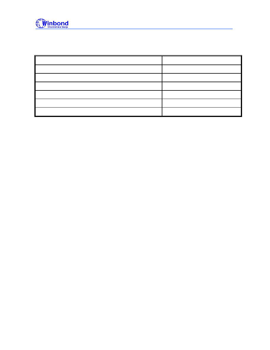
W81282F
PRELIMINARY
Publication Release Date: Aug. 199
9
- 6 -
Revision 0.5
59
XRD# (P37)
IOUD2
Port 3.7
.This pin is dedicated for internal use.
U
60
OVRI2#
IUD2T
Downstream port2 over-current status input. Active low.
-
61
XWR# (P36)
IOUD2
Port 3.6
.This pin is dedicated for internal use.
U
62
P35
IOUD2
Port 3.5
and reverse for input or output application.
U
63
UPWEN2#
O2
Downstream port2 power control. Active low.
-
64
SO20 (P34)
IOUD2
Port 3.4 and function of
Scan Out line 20.
U
65
SO1
9
O2
This pin is function of Scan Out line 1
9
.
-
66,67
GND
Power0
Digital ground.
-
68
N.C.
IOUD2
No connection. This pin should be floated.
U
69
SO08 (P20)
IOUD2
Port 2.0 and function of Scan Out line 8.
U
70
OVRI1#
IUD2T
Downstream port1 over-current status input. Active low.
-
71
SO09 (P21)
IOUD2
Port 2.1 and function of Scan Out line 9.
U
72
UPWEN1#
O2
Downstream port1 power control. Active low.
-
73
SO10 (P22)
IOUD2
Port 2.2 and function of Scan Out line 10.
U
74
FWKP5#
IUD2
Embedded function wake-up input.
Can be used for Wake-up hot key.
D
75
SO11 (P23)
IOUD2
Port 2.3 and function of Scan Out line 11.
U
76
EECLK/IDSEL0
(P30)
IOUD2
This pin is Port 3.0 and function of serial clock line interfacing
with external EEPROM. If no serial EEPROM present, this
pin is used to scan ID selection and named IDSEL0.
U
77
SO12 (P24)
IOUD2
Port 2.4 and function of Scan Out line 12.
U
78
SO13 (P25)
IOUD2
Port 2.
5
and function of Scan Out line 13.
U
79,80
GND3V
Power0
Ground of port3 and port4 transceivers.
-
81
DP4
AIO
USB D+ for downstream port4.
-
82
DM4
AIO
USB D- for downstream port4.
-
83,84
N.C.
-
No connection.
85
DP3
AIO
USB D+ for downstream port3.
-
86
DM3
AIO
USB D- for downstream port3.
-
87
N.C.
-
No connection.
88,89
GND3V
Power0
Ground of port1 and port2 transceivers.
-
90
DP2
AIO
USB D+ for downstream port2.
-
91
DM2
AIO
USB D- for downstream port2.
-
W81282F
PRELIMINARY
Publication Release Date: Aug. 199
9
- 7 -
Revision 0.5
92,93
N.C.
-
No connection.
94
DP1
AIO
USB D+ for downstream port1.
-
95
DM1
AIO
USB D- for downstream port1.
-
96,97
GND3V
Power0
Ground of port0 transceivers.
-
98
N.C.
-
No connection.
99
DP0
AIO
USB D+ for upstream port0.
-
100
DM0
AIO
USB D- for upstream port0.
-
W81282F
PRELIMINARY
Publication Release Date: Aug. 199
9
- 8 -
Revision 0.5
6. ABSOLUTE MAXIMUM RATINGS
PARAMETER
LIMIT
Supply Voltage (Vcc to Vss)
5.5V
Analog Input Voltage
Vss-0.5V to Vcc+0.5V
Digital Input Voltage
Vss-0.5V to Vcc+0.5V
Power Dissipation
TBD
Ambient Operating Temperature
0
o
C to 70
o
C
Lead Temperature (Soldering, 10 sec)
250
o
C
W81282F
PRELIMINARY
Publication Release Date: Aug. 199
9
- 9 -
Revision 0.5
7. ELECTRICAL CHARACTERISTICS
Operating conditions: VCC = 5V +/-5%, Ta=0
o
to 70
o
C
PARAMETER
Symbol
Conditions
Min Max Unit
VCC Supply Current
Icc
TBD mA
Logic Output High
VOH
Io>24ma
2.5
VCC V
Logic Output Low
VOL
Io>6ma
0.4
V
Logic Input Leakage Current
Ta=70
o
C
10
uA
USB CHARACTERISTICS
Note 8
Leakage Current:
Hi-Z State Output Leakage
ILO
V< V IN <3.3 V
-10 +10 uA
Input Levels:
Differential Input Sensitivity
VDI
|(D+)-(D-)|
0.2
V
Single Ended Signal "0"
VSE0
0.8 2.0 V
Differential Common Mode Range
V
CM
Includes VDI range 0.8 2.5
Output Levels:
Driver Output Low
VOLU RL of 1.5 k
to 3.6 V
0.3 V
Driver Output High
VOHU RL of 15 k
to GND 2.8 3.6 V
Output Signal Crossover Voltage
V
CRS
1.3 2.0 V
Capacitance:
Transceiver Capacitance
CIN
Pin to GND
20 pF
Full Speed Timings:
Output Rise/Fall Times
t R /t F Note 1, 4 (C
L
= 50 pF) 4 20 ns
Source Differential Driver Jitter to Next Transition
/ to Paired Transition
t DJ1
/tDJ2
Note 2, 3
-3.5
/-4
3.5
/4
ns
ns
Differential to EOP transition Skew
t
DEOP
Note 3
-2
5
ns
Hub Differential Data Delay(without cable)
t HDD2 Note 2,3,5
44 ns
Hub Differential Driver Jitter to Next Transition
/ to Paired Transition (including cable)
t HDJ1
/ t
HDJ2
Note 2,3,5
-3
/ -1
3
/1
ns
Data bit width distortion after SOP
t SOP Note 3,5
-5
5
ns
Hub SE0 Delay Relative to t
HDD
t EOPD Note 3,5
0 15 ns
Hub EOP Output Width Skew
t HESK Note 3,5
-15 15 ns
Low Speed Timings:
Output Rise/Fall Times
t R /t F Note 1, 4 (C
L
= 50 pF) 75 300 ns
W81282F
PRELIMINARY
Publication Release Date: Aug. 199
9
- 10 -
Revision 0.5
7. ELECTRICAL CHARACTERISTICS, continued
PARAMETER
Symbol
Conditions
Min Max Unit
Source Differential Driver Jitter to Next Transition
/ to Paired Transition
t DJ1
/tDJ2
Note 2, 3
-25
/-14
25
/14
ns
ns
Differential to EOP transition Skew
t
DEOP
Note 3
-40 100 ns
Hub Differential Data Delay(without cable)
t HDD2 Note 2,3,5
300 ns
Hub Differential Driver Jitter to Next Transition
/ to Paired Transition (including cable)
t HDJ1
/ t
HDJ2
Note 2,3,5
-45
/ -45
45
/-45
ns
Data bit width distortion after SOP
t SOP Note 3,5
-60 60 ns
Hub SE0 Delay Relative to t
HDD
t EOPD Note 3,5
0 200 ns
Hub EOP Output Width Skew
t HESK Note 3,5
-300 300 ns
Note 1: Measured from 10% to 90% of the data signal.
Note 2: Timing difference between the differential signals.
Note 3: Measured at crossover point of differential data signals.
Note 4: The rising and falling edges should be smoothly transiting(monotonic)
Note 5: Full Speed timing have a 1.5 k
pull-up to 2.8 V on the D+ (DP) data line.
Note 6: Low Speed timing have a 1.5 k
pull-up to 2.8 V on the D- (DM) data line.
Note 7: The maximum load specification is the maximum effective capacitive load allowed that meets
the target hub VBUS droop of 330 mV.
Note 8: All other USB Electrical Characteristics refer to USB spec Rev 1.1 7.3.2 and 7.3.3.

W81282F
PRELIMINARY
Publication Release Date: Aug. 199
9
- 11 -
Revision 0.5
8. TYPICAL APPLICATION
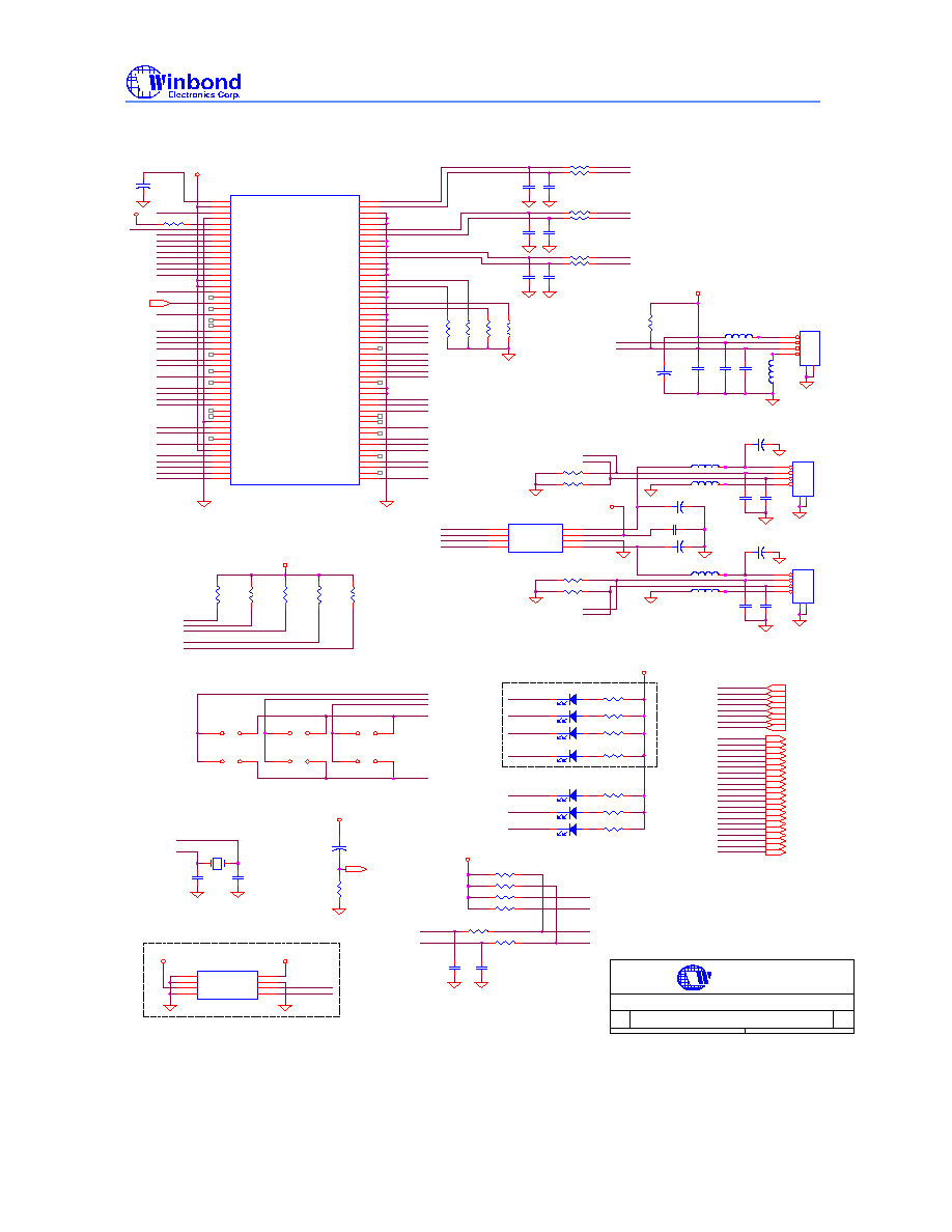
W81282F
PRELIMINARY
Publication Release Date: Aug. 199
9
- 12 -
Revision 0.5
282DEMO1.SCH
1.0
W81282F Reference Schematic
1
1
Thursday, August 19, 1999
Title
Size
Document Number
Rev
Date:
Sheet
of
VCC
VCC
VCC
VCC
VCC
VCC
VCC
VCC
VCC
VCC
CD-
CD+
OCP3
CD-
SO14
CD1-
OCP4
CD+
CD1+
SO15
LEDNUM
OCP1
SI0
LEDCAP
OCP2
SI1
LEDSCR
CD2-
SI2
CD2+
LEDOVC
SI3
SI4
SO16
SO13
EESDA
SO12
SI5
EESCL
SI6
SO11
SI7
SO10
SO17
PWEN1
GANGED
SO09
OCP1
VOLA
SO08
VOLB
LEDEN2
PLLE
SO19
LEDEN1
SO20
PWEN2
X1
OCP2
X2
SO07
SO00
LEDEN0
SO06
SO01
SO02
SO05
SO16
SO18
OCP3
SO18
SO03
SO19
OCP4
SO04
GANGED
PLLE
SI0
SI1
SI2
SI3
LEDEN0
SI4
SI5
SI6
LEDEN1
SI7
LEDNUM
LEDCAP
SO00
LEDSCR
LEDEN2
SO01
SO02
X1
EESCL
SO03
SO04
X2
LEDOVC
SO05
SO06
SO07
SO08
SO09
SO10
SO11
LEDNUM
SO12
SO13
EESDA
SO14
LEDCAP
SO15
SO16
SO17
LEDSCR
SO18
SO19
SO20
EESCL
EESDA
PW1
CD1-
CD1+
PW2
PWEN2
CD2-
CD2+
PWEN1
FL1
FL2
FL1
FL2
U1
24LC04B
1
2
3
4
5
6
7
8
A0
A1
A2
VSS
SDA
SCL
RC
VCC
R1
470
R2
470
R3
470
R4
470
R5
470
R6
470
R7
470
R8
8.2K
+
C1
10u
+
C2
10u
Y1
12M
U2
W81282F-100QFP
1
2
3
4
5
6
7
8
9
10
11
12
13
14
15
16
17
18
19
20
21
22
23
24
25
26
27
28
29
30
31
32
33
34
35
36
37
38
39
40
41
42
43
44
45
46
47
48
49
50
51
52
53
54
55
56
57
58
59
60
61
62
63
64
65
66
67
68
69
70
71
72
73
74
75
76
77
78
79
80
81
82
83
84
85
86
87
88
89
90
91
92
93
94
95
96
97
98
99
100
VDD3V
VDDA
SO14/P26
GNDA
VBUS
SO15/P27
LED0#
SI0/P10
LED1#
SI1/P11
LED2#
SI2/P12
LEDOVR#
SI3/P13
VDD
VDD
SI4/P14
PSEN#
RESET
INPUT_P
SO16
PSDA/P33
P32/XINT#
IDSEL1/EESDA
SI5/P15
SI6/P16
SI7/P17
BUSPWR#
SO17
GANGED#
LEDEN4#
VOLUME_A
LEDEN3#
VOLUME_B
LEDEN2#
PLLE
LEDEN1#
XCVREN
UC51E
GND
XTAL1
XTAL2
ROMEN
SO00/P07
VDD
SO01/P06
SO02/P05
SO18
SO03/P04
OCP4#
SO04/P03
PWEN4#
OCP3#
SO05/P02
PWEN3#
SO06/P01
LEDEN0#
SO07/P00
XRD#/P37
OCP2#
XWR#/P36
PSCLK/P35
PWEN2#
SO20/P34
SO19
GND
GND
XALE
SO08/P20
OCP1#
SO09/P21
PWEN1#
SO10/P22
FWKP5#
SO11/P23
IDSEL0/EESCL
SO12/P24
SO13/P25
GND3V
GND3V
D4+
D4-
NC
NC
D3+
D3-
NC
GND3V
GND3V
D2+
D2-
NC
NC
D1+
D1-
GND3V
GND3V
NC
D+
D-
R9
10K
D1
EN0
D2
EN1
D3
EN2
JP1
JUMPER
JP2
JUMPER
JP3
JUMPER
JP5
JUMPER
C3
30p
C4
30p
D4
NUMLK
D5
CAPLK
D6
SCRLK
D7
OVC
R15
30
R16
30
C10
15p
C11
15p
R17
30
R18
30
C12
15p
C13
15p
R19
30
R20
30
C14
15p
C15
15p
R21
10K
+
CT1
10u
L5
FB
C16
0.1u
R22
7.5K
R23
10K
R24
10K
R25
10K
R26
10K
C17
0.1u
C18
0.1u
R27
10K
R28
15K
R29
15K
R30
15K
R31
15K
R32
100K
R33
100K
R34
100K
C30
47pF
C31
47pF
JP4
JUMPER
JP6
JUMPER
R35
100K
R36
100K
inbond
WINBOND ELECTRONICS CORP_
U4
AIC1526-0
1
2
3
4
8
7
6
5
C/A
F/A
F/B
C/B
O/A
IN
GND
O/B
C26
47pF
L2
FB(30ohm)
USB2
USB(A)
1
2
3
4
5
6
USB3
USB(A)
1
2
3
4
5
6
L1
FB(30ohm)
L4
FB(30ohm)
C29
47pF
L3
FB(30ohm)
R14
15K
C28
47pF
C7
0.1u
R12
15K
+
C9
0.1u
+
C6
120u
R11
15K
C27
47pF
R13
15K
+
C5
120u
+
C8
0.1u
USB1
UP-PORT
1
2
3
4
5
6
L6
FB
RESET
RESET
SI1
SI2
SI3
SI4
SI5
SI6
SI7
SO01
SO02
SO03
SO04
SO05
SO06
SO07
SO08
SO09
SO10
SO11
SO12
SO13
SO14
SO15
SO16
SO17
SO18
SO19
SO20
SO00
SI0
W81282F Reference Schematic
Option
Place R15 ~ R20 & C10 ~ C15
as close as W81282F
Option
W81282F
PRELIMINARY
Publication Release Date: Aug. 199
9
- 13 -
Revision 0.5
9. HOW TO READ THE TOP MARKING
Example: The top marking of W81282F-05
1st line: Winbond logo
2nd line: the type number: W81282F-05
3rd line: the tracking code: 732 A C 2 7242968
732: packages made in '97, week 19
A: assembly house ID; A means ASE, S means SPIL ... etc
C: IC revision; B means version B, C means version C
2: wafers manufactured in Winbond FAB 2
7242968: wafer production series lot number
inbond
W81282F-05
732AC27242968

W81282F
PRELIMINARY
Publication Release Date: Aug. 199
9
- 14 -
Revision 0.5
10. PACKAGE DIMENSIONS
(100-pin QFP)
51
50
31
30
1
80
81
100
2
1
A
H
D
D
e
b
E H
E
y
A
A
Seating Plane
L
L
1
See Detail F
Detail F
c
1. Dimension D & E do not include interlead
flash.
2. Dimension b does not include dambar
protrusion/intrusion.
3. Controlling dimension: Millimeters
4. General appearance spec. should be based
on final visual inspection spec.
0.10
0
12
0
0.004
3.30
0.10
0.130
0.004
Notes:
Symbol
Min. Nom. Max.
Max.
Nom.
Min.
Dimension in inches
Dimension in mm
12
2.40
1.40
19.10
1.20
18.80
1.00
18.49
0.094
0.055
0.988
0.752
0.047
0.976
0.740
0.039
0.964
0.728
0.65
20.13
14.13
0.25
0.40
2.97
20.00
14.00
2.85
19.87
13.87
0.10
0.25
2.73
0.792
0.556
0.010
0.016
0.117
0.787
0.551
0.112
0.026
0.782
0.546
0.004
0.010
0.107
0.012
0.006
0.15
0.30
24.49
24.80
25.10
0.020
0.087
0.032
0.103
0.50
0.80
2.21
2.62
A
b
c
D
e
H
D
H
E
L
y
A
A
L
1
1
2
E
q
q

W81282F
PRELIMINARY
Publication Release Date: Aug. 199
9
- 15 -
Revision 0.5
Headquarters
No. 4, Creation Rd. III
Science-Based Industrial Park
Hsinchu, Taiwan
TEL: 886-35-770066
FAX: 886-35-789467
www: http://www.winbond.com.tw/
Taipei Office
11F, No. 115, Sec. 3, Min-Sheng East Rd.
Taipei, Taiwan
TEL: 886-2-7190505
FAX: 886-2-7197502
TLX: 16485 WINTPE
Winbond Electronics (H.K.) Ltd.
Rm. 803, World Trade Square, Tower II
123 Hoi Bun Rd., Kwun Tong
Kowloon, Hong Kong
TEL: 852-27516023-7
FAX: 852-27552064
Winbond Electronics
(North America) Corp.
2730 Orchard Parkway
San Jose, CA 95134 U.S.A.
TEL: 1-408-9436666
FAX: 1-408-9436668
Please note that all data and specifications are subject to change without notice. All
the trade marks of products and companies mentioned in this data sheet belong to
their respective owners.