
Publication Release Date: April 13, 2005
- I -
Revision 1.1
W83176R-732
Data Sheet
WINBOND
2 DIMM DDR ZERO
DELAY BUFFER
FOR
SIS CHIPSET

W83176R-732
- II -
Table of Contents-
1.
GENERAL DESCRIPTION ..........................................................................................................1
2.
FEATURES ..................................................................................................................................1
3.
PIN CONFIGURATION ................................................................................................................1
4.
BLOCK DIAGRAM .......................................................................................................................2
5.
PIN DESCRIPTION......................................................................................................................2
5.1
Clock Outputs...........................................................................................................................3
5.2
Power Pins................................................................................................................................3
6.
REGISTER 0 ~ REGISTER 4 RESERVED .................................................................................4
6.1
Register 5: Output Control (1 = Active, 0 = Inactive) (Default = FFh).....................................4
6.2
Register 6: Output Control (1 = active, 0 = inactive) (Default = FFh) .....................................4
7.
ACCESS INTERFACE .................................................................................................................5
7.1
Block Write Protocol.................................................................................................................5
7.2
Block Read Protocol.................................................................................................................5
7.3
Byte Write Protocol...................................................................................................................5
7.4
Byte Read Protocol ..................................................................................................................5
8.
SPECIFICATIONS .......................................................................................................................6
8.1
Absolute Maximum Ratings .....................................................................................................6
8.2
A.C. Characteristics..................................................................................................................6
8.3
D.C. Characteristics .................................................................................................................6
9.
ORDERING INFORMATION........................................................................................................7
10.
HOW TO READ THE TOP MARKING.........................................................................................7
11.
PACKAGE DRAWING AND DIMENSIONS.................................................................................8
12.
REVISION HISTORY ...................................................................................................................9

W83176R-732
Publication Release Date: April 13, 2005
- 1 -
Revision 1.1
1. GENERAL DESCRIPTION
The W83176R-732 is a 2.5V Zero-delay D.D.R. Clock buffer designed for SiS chipset. W83176R-732
can support 2 D.D.R. DRAM DIMMs.
The W83176R-732 provides I
2
C serial bus interface to program the registers to enable or disable each
clock outputs. The W83176R-732 accepts a reference clock as its input and runs on 2.5V supply.
2. FEATURES
�
Zero-delay clock outputs
�
Feedback pins for synchronous
�
Supports up to 2 D.D.R. DIMMs
�
One pairs of additional outputs for feedback
�
Low Skew outputs (< 100 pS)
�
Supports 400 MHz D.D.R. SDRAM
�
2
C 2-Wire serial interface and supports Byte or Block Date RW
�
Packaged in 28-pin SSOP
3. PIN CONFIGURATION
*: Internal pull-up resistor 120K to VDD

W83176R-732
- 2 -
4. BLOCK DIAGRAM
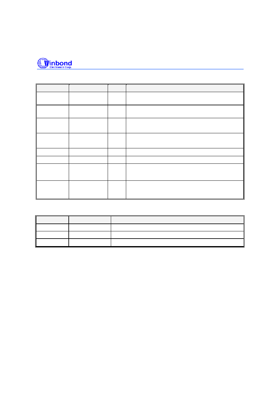
5. PIN DESCRIPTION
BUFFER TYPE
SYMBOL
DESCRIPTION
IN Input
OUT Output
I/O Bi-directional
Pin
*
Internal 120K
pull-up
NC Not
connect
W83176R-732
Publication Release Date: April 13, 2005
- 3 -
Revision 1.1
5.1
Clock Outputs
PIN
PIN NAME
TYPE
DESCRIPTION
27, 25, 16,
14, 5, 1
CLKC [5:0]
OUT Complementary Clocks of differential pair outputs
26, 24, 17,
13, 4, 2
CLKT [5:0]
OUT True Clocks of differential pair outputs
22 SDATA
*
I/O
Serial data of I
2
C 2-wire control interface
Internal pull-up resistor 120K to VDD
7 SCLK
*
IN
Serial clock of I
2
C 2-wire control interface
Internal pull-up resistor 120K to VDD
8 CLK_INT
IN
True reference clock input, 3.3V tolerant input
9, 18, 21
N/C
NC
Not connected
19
FB_OUTT
OUT
True Feedback output, dedicated for external feedback.
It switches at the same frequency as the CLK. This
output must be wired to FB_INT.
20
FB_INT
IN
True Feedback input, provides feedback signal to the
internal PLL for synchronization with CLK_INT to
eliminate phase error.
5.2 Power Pins
PIN
PIN NAME
DESCRIPTION
6, 11, 15, 28
GND
Ground
3, 12, 23
VDD
Power supply 2.5V
10
AVDD Analog
power
supply,
2.5V

W83176R-732
- 4 -
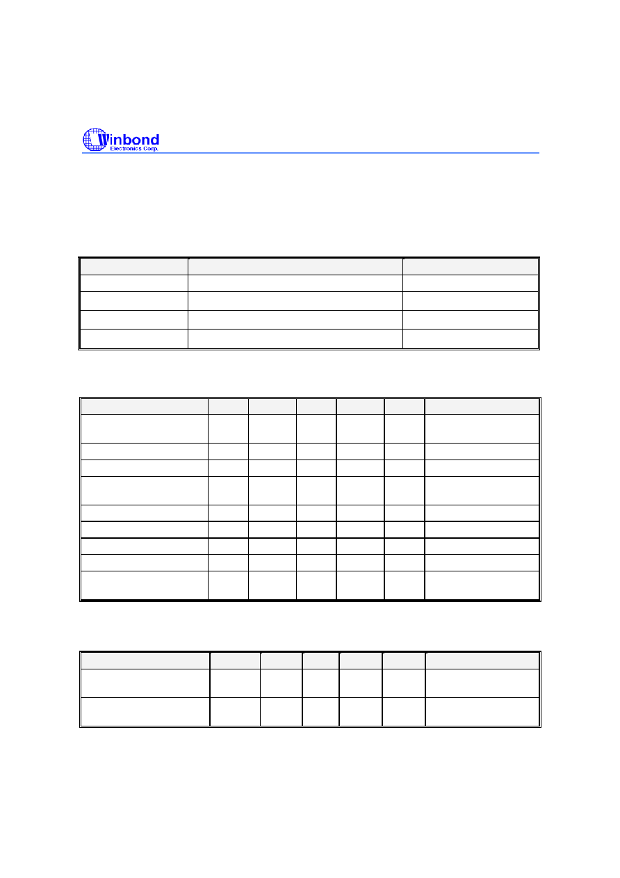
6. REGISTER 0 ~ REGISTER 4 RESERVED
6.1 Register 5: Output Control (1 = Active, 0 = Inactive) (Default = FFh)
BIT
@POWERUP
PIN
DESCRIPTION
7
1
1, 2
CLKC0, CLKT0 (Active/Inactive)
6
1
5, 4
CLKC1, CLKT1 (Active/Inactive)
5 1 -
Reserved
4 1 -
Reserved
3
1
14, 13
CLKC2, CLKT2 (Active/Inactive)
2
1
16, 17
CLKC3, CLKT3 (Active/Inactive)
1 1 -
Reserved
0 1 -
Reserved
6.2 Register 6: Output Control (1 = active, 0 = inactive) (Default = FFh)
BIT
@POWERUP
PIN
DESCRIPTION
7 1 -
Reserved
6 1 -
Reserved
5 1 -
Reserved
4 1 -
Reserved
3
1
25, 24
CLKC4, CLKT4 (Active/Inactive)
2 1 -
Reserved
1
1
27, 26
CLKC5, CLKT5 (Active/Inactive)
0 1 -
Reserved
W83176R-732
Publication Release Date: April 13, 2005
- 5 -
Revision 1.1
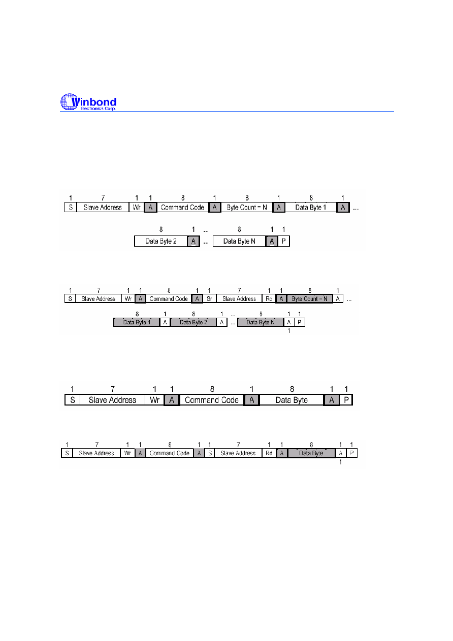
7. ACCESS INTERFACE
The W83176R-732 provides I
2
C Serial Bus for microprocessor to read/write internal registers. In the
W83176R-732 is provided Block Read/Block Write and Byte-Data Read/Write protocol. The I
2
C write
address is defined at 0xD4. The I
2
C read address is defined at 0xD5.
7.1 Block Write Protocol
7.2 Block Read Protocol
## In block mode, the command code must filled `00h'
7.3 Byte Write Protocol
7.4 Byte Read Protocol
W83176R-732
- 6 -
8. SPECIFICATIONS
8.1 Absolute Maximum
Ratings
Stresses greater than those listed in this table may cause permanent damage to the device.
Precautions should be taken to avoid application of any voltage higher than the maximum rated
voltages to this circuit. Maximum conditions for extended periods may affect reliability. Unused inputs
must always be tied to an appropriate logic voltage level (Ground or VDD).
SYMBOL
PARAMETER
RATING
VDD, AVDD
Voltage on any pin with respect to GND
-0.5V to +3.6V
T
STG
Storage Temperature
-65
�
C to +150
�
C
T
B
Ambient Temperature
-55
�
C to +125
�
C
T
A
Operating Temperature
0
�
C to +70
�
C
8.2 A.C. Characteristics
VDD = AVDD = 2.5V
�
5 %, T
A
= 0
�
C to +70
�
C, Test load = 10 pF
PARAMETER
SYM.
MIN.
TYP.
MAX.
UNITS
TEST CONDITIONS
Operating Clock
Frequency
F
IN
100 200
MHz
Input Clock Duty Cycle
Dtin
40
60
%
Dynamic Supply Current
Idd
300
mA
Fin = 100 to 200 MHz
Cycle to Cycle Jitter
C-
Cjitter
200
pS
Fout = 100 to 200 MHz
Output to Output Skew
Tskew
100
pS
Fout = 100 to 200 MHz
Output Clock Rise Time
Tor
650
950
pS
Fout = 100 to 200 MHz
Output Clock Fall Time
Tof
650
950
pS
Fout = 100 to 200 MHz
Output Clock Duty Cycle
Dtot
45
55
%
Fout = 100 to 200 MHz
Output Differential-pair
Crossing Voltage
Voc
(VDD/2)
-0.2
VDD/
2
(VDD/2)
+ 0.2
V
Fout = 100 to 200 MHz
8.3 D.C. Characteristics
VDD = AVDD= 2.5V
�
5 %, T
A
= 0
�
C to +70
�
C
PARAMETER
SYM.
MIN.
TYP.
MAX.
UNITS
TEST CONDITIONS
SDATA, SCLK Input Low
Voltage
SV
IL
1.0
V
dc
SDATA, SCLK Input High
Voltage
SV
IH
2.2 V
dc
W83176R-732
Publication Release Date: April 13, 2005
- 7 -
Revision 1.1
D.C. Characteristics, continued.
PARAMETER
SYM.
MIN.
TYP.
MAX.
UNITS
TEST CONDITIONS
CLKIN, FBIN Input Voltage
Low
V
IL
0.4
V
dc
Fin = 100 to 200 MHz
CLKIN, FBIN Input Voltage
High
V
IH
2.1 V
dc
Fin = 100 to 200 MHz
Input Pin Capacitance
C
IN
5 pF
Output Pin Capacitance
C
OUT
6 pF
Input Pin Inductance
L
IN
7 nH
9. ORDERING INFORMATION
PART NUMBER
PACKAGE TYPE
PRODUCTION FLOW
W83176R_732
28-pin SSOP
Commercial, 0
�
C to +70
�
C
10. HOW TO READ THE TOP MARKING
1st line: Winbond logo and the type number: W83176R-732
2nd line: Tracking code 2 8051234
2: wafers manufactured in Winbond FAB 2
8051234: wafer production series lot number
3rd line: Tracking code 342 G B
342: packages made in '2003, week 42
G: assembly house ID; O means OSE, G means GR
B: IC revision
All the trade marks of products and companies mentioned in this data sheet belong to their
respective owners.
W83176R-732
28051234
342GB
W83176R-732
- 8 -
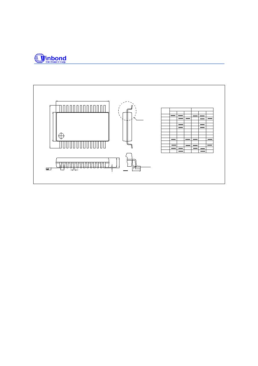
11. PACKAGE DRAWING AND DIMENSIONS
28-pin 209 mil
1
2
D
E
e
Y
b
A1
A2 A
SEATING PLANE
DTEAIL A
L
L1
DETAIL A
SEATING PLANE
E
H
14
15
0
0.002
0.197
0.291
7.80
0
7.40
8
8.20
5.30
b
E
D
c
9.90
5.00
A1
A2
A
5.60
10.50
10.20
2.00
1.85
8
0.323
0.307
0.073
0.079
0.220
0.389
0.413
0.401
0.209
MIN.
DIMENSION IN INCH
SYMBOL
DIMENSION IN MM
MIN.
NOM
MAX.
MAX.
NOM
0.05
e
L
L1
Y
0.009
0.015
0.004
0.010
0.021 0.030
0.050
0.004
0.22
0.38
0.09
0.25
0.65
0.0256
0.55
0.75
1.25
0.10
H
E
0.95
0.037
1.75
1.65
0.065 0.069
W83176R-732
Publication Release Date: April 13, 2005
- 9 -
Revision 1.1
12. REVISION HISTORY
VERSION DATE
PAGE
DESCRIPTION
All of the versions before 0.50 are for internal
use.
0.5
12/18/03
n.a.
First published preliminary version
1.0 05/06/04
Update
on
web
1.1 04/13/2005
9 Add
disclaimer
Important Notice
Winbond products are not designed, intended, authorized or warranted for use as components
in systems or equipment intended for surgical implantation, atomic energy control
instruments, airplane or spaceship instruments, transportation instruments, traffic signal
instruments, combustion control instruments, or for other applications intended to support or
sustain life. Further more, Winbond products are not intended for applications wherein failure
of Winbond products could result or lead to a situation wherein personal injury, death or
severe property or environmental damage could occur.
Winbond customers using or selling these products for use in such applications do so at their
own risk and agree to fully indemnify Winbond for any damages resulting from such improper
use or sales.
Headquarters
No. 4, Creation Rd. III,
Science-Based Industrial Park,
Hsinchu, Taiwan
TEL: 886-3-5770066
FAX: 886-3-5665577
http://www.winbond.com.tw/
Taipei Office
TEL: 886-2-8177-7168
FAX: 886-2-8751-3579
Winbond Electronics Corporation America
2727 North First Street, San Jose,
CA 95134, U.S.A.
TEL: 1-408-9436666
FAX: 1-408-5441798
Winbond Electronics (H.K.) Ltd.
No. 378 Kwun Tong Rd.,
Kowloon, Hong Kong
FAX: 852-27552064
Unit 9-15, 22F, Millennium City,
TEL: 852-27513100
Please note that all data and specifications are subject to change without notice.
All the trade marks of products and companies mentioned in this data sheet belong to their respective owners.
Winbond Electronics (Shanghai) Ltd.
200336 China
FAX: 86-21-62365998
27F, 2299 Yan An W. Rd. Shanghai,
TEL: 86-21-62365999
Winbond Electronics Corporation Japan
Shinyokohama Kohoku-ku,
Yokohama, 222-0033
FAX: 81-45-4781800
7F Daini-ueno BLDG, 3-7-18
TEL: 81-45-4781881
9F, No.480, Rueiguang Rd.,
Neihu District, Taipei, 114,
Taiwan, R.O.C.