
Publication Release Date: April 13, 2005
- I - Revision 1.1
W83194BR-372
WINBOND
CLOCK GENERATOR
FOR SIS 746/748 CHIPSETS

W83194BR-372
- II -
Table of Contents-
1.
GENERAL DESCRIPTION ......................................................................................................... 1
2.
PRODUCT FEATURES .............................................................................................................. 1
3.
PIN CONFIGURATION ............................................................................................................... 2
4.
BLOCK DIAGRAM ...................................................................................................................... 2
5.
PIN DESCRIPTION..................................................................................................................... 3
5.1
Crystal I/O .............................................................................................................................3
5.2
CPU, AGP, ZCLK and PCI, IOAPIC Clock Outputs............................................................3
5.3
Fixed Frequency Outputs.....................................................................................................4
5.4
I
2
C Control Interface .............................................................................................................4
5.5
Power Management Pins.....................................................................................................4
5.6
Power Pins............................................................................................................................4
6.
FREQUENCY SELECTION BY HARDWARE OR SOFTWARE ................................................ 5
7.
I
2
C CONTROL AND STATUS REGISTERS............................................................................... 6
7.1
Register 0: Frequency Select (Default = 40h) .....................................................................6
7.2
Register 1: CPU Clock (1 = Enable, 0 = Stopped) (Default: 68h).......................................6
7.3
Register 2: PCI Clock (1 = Enable, 0 = Stopped) (Default: FFh)........................................6
7.4
Register 3: AGP, 24_48MHz, 48MHz, REF Control (1 =Enable, 0 =Stopped) (Default:
FFh) 7
7.5
Register 4: IOAPIC, ZCLK Control (1 = Enable, 0 = Stopped) (Default: F0h) ...................7
7.6
Register 5: 24_48MHz Control (Default: 88h) .....................................................................7
7.7
Register 6: M/N (Default: 90h) .............................................................................................8
7.8
Register 7: N (Default: BBh).................................................................................................8
7.9
Register 8: Winbond Chip ID (Default: 72h) (Read only)....................................................8
7.10
Register 9: Reserved (Default: 50h) (Read only) ................................................................9
7.11
Register 10: M/N Program (Default: 04h)............................................................................9
7.12
Register 11: Spread Spectrum Programming (Default: 0Eh) ...........................................10
7.13
Register 12: Divisor and Step-less Enable Control (Default: 88h)....................................10
7.14
Register 13: FIX Mode Control (Default: 0Fh)...................................................................12
7.15
Register 14: Fix Mode Control (Default: 2Ch) ...................................................................12
7.16
Register 15: Skew Control (Default: E4h)..........................................................................13
8.
ACCESS INTERFACE .............................................................................................................. 14
8.1
Block Write Protocol ...........................................................................................................14
8.2
Block Read Protocol...........................................................................................................14

W83194BR-372
Publication Release Date: April 13, 2005
- III - Revision 1.1
8.3
Byte Write Protocol.............................................................................................................14
8.4
Byte Read Protocol.............................................................................................................14
9.
SPECIFICATIONS .................................................................................................................... 15
9.1
Absolute Maximum Ratings ...............................................................................................15
9.2
General Operating Characteristics ....................................................................................15
9.3
Skew Group Timing Clock .................................................................................................15
9.4
CPU (Open Drain) Electrical Characteristics.....................................................................16
9.5
AGP, ZCLK Electrical Characteristics................................................................................16
9.6
PCI Electrical Characteristics.............................................................................................16
9.7
24M, 48M Electrical Characteristics ..................................................................................17
9.8
REF Electrical Characteristics............................................................................................17
9.9
IOAPIC Electrical Characteristics ......................................................................................17
10.
ORDERING INFORMATION..................................................................................................... 18
11.
HOW TO READ THE TOP MARKING...................................................................................... 18
12.
PACKAGE DRAWING AND DIMENSIONS.............................................................................. 19
13.
REVISION HISTORY ................................................................................................................ 20


W83194BR-372
Publication Release Date: April 13, 2005
- 1 - Revision 1.1
1. GENERAL DESCRIPTION
The W83194BR-372 is a Clock Synthesizer for SIS 746/748 chipset. W83194BR-372 provides all
clocks required for high-speed microprocessor and provides step-less frequency programming and 32
different frequencies of CPU, PCI, and AGP clocks setting, support two ZCLK clock outputs; all clocks
are externally selectable with smooth transitions.
The W83194BR-372 provides I
2
C serial bus interface to program the registers to enable or disable
each clock outputs and provides -0.5% and +/-0.25% center type spread spectrum or programmable
S.S.T. scale to reduce EMI.
The W83194BR-372 accepts a 14.318 MHz reference crystal as its input and runs on a 3.3V supply.
2. PRODUCT FEATURES
�
1 2.5V open drain Differential pairs clock outputs for CPU
�
1 2.5V open drain singled-ended clock output for chipset host bus.
�
2 3.3V ZCLK clock outputs
�
2 AGP clock outputs
�
8 PCI synchronous clocks
�
2 2.5V IOAPIC clock outputs
�
1 24_48Mhz clock output for super I/O.
�
1 48 MHz clock output for USB.
�
3 14.318MHz REF clock outputs.
�
ZCLK/AGP/PCI clock out supports synchronous and asynchronous mode
�
Smooth frequency switch with selections from 100 to 200MHz
�
Step-less frequency programming
�
I
2
C 2-Wire serial interface and support byte read/write and block read/write.
�
-0.5% and +/- 0.25% center type spread spectrum
�
Programmable S.S.T. scale to reduce EMI
�
Programmable registers to enable/stop each output and select modes
�
Programmable clock outputs Skew control
�
48-pin SSOP package

W83194BR-372
- 2 -
3. PIN CONFIGURATION
1
2
3
4
5
6
7
8
9
10
11
12
13
14
15
16
17
18
19
20
21
22
23
24
48
47
46
45
44
43
42
41
40
39
38
37
36
35
34
33
32
31
30
29
28
27
26
25
VDDREF
FS0
&
/REF0
FS1
&
/REF1
REF2
GND
XIN
XOUT
GND
ZCLK0
ZCLK1
VDDZ
PCI_STOP#*
VDDPCI
FS2
&
/PCI_F0
FS3*/PCI_F1
PCI0
PCI1
GND
VDDPCI
PCI2
PCI3
PCI4
PCI5
GND
VDDI
IOAPIC1
IOAPIC0
GND
CPU_STOP#*
CPUT1
VDDCPU
GND
CPUT0
CPUC0
VDDCPU
GND
VDDA
SCLK *
SDATA*
PD#*
GND
AGP_0
AGP_1
VDDAGP
VDD48
48MHz
24_48MHz
GND
#: Active low
*: Internal pull up resistor 120K to VDD
&: Internal Pull-down resistor 120K to GND
4. BLOCK DIAGRAM
PLL2
XTAL
OSC
PLL1
Spread
Spectrum
M/N/Ratio
ROM
Latch
&POR
Control
Logic
&Config
Register
I2C
Interface
Divider
VCOCLK
48MHz
REF 0:2
CPUT0:1
CPUC0
IOAPIC0:1
AGP 0:1
PCI_F0:1,P
CI_0:5
XIN
XOUT
FS(0:3)
PD#*
SDATA*
SCLK*
2
8
Divider
24_48MHz
2
3
2
ZCLK0:1
2
PCI_STOP#*
CPU_STOP#*

W83194BR-372
Publication Release Date: April 13, 2005
- 3 - Revision 1.1
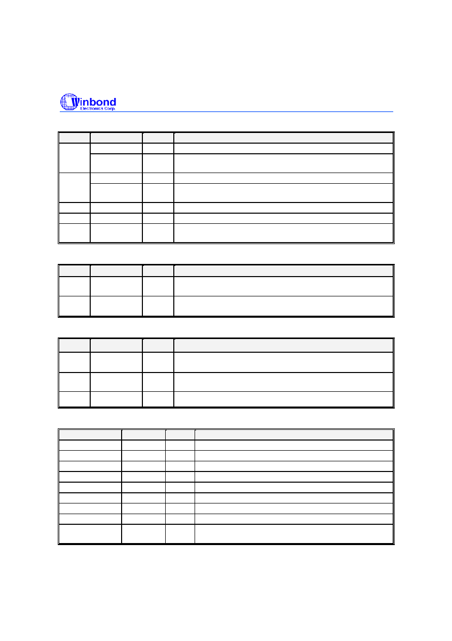
5. PIN DESCRIPTION
BUFFER TYPE SYMBOL
DESCRIPTION
IN Input
IN
tp120k
Latched input at power up, internal 120k pull up.
IN
td120k
Latched input at power up, internal 120k pull down.
OUT Output
OD Open
Drain
# Active
Low
*
Internal 120k
pull-up
&
Internal 120 k
pull-down
5.1 Crystal I/O
PIN
PIN NAME
TYPE
DESCRIPTION
6 XIN
IN
Crystal input with internal loading capacitors (18pF) and
feedback resistors.
7 XOUT
OUT
Crystal output at 14.318MHz nominally with internal loading
capacitors (18pF).
5.2 CPU, AGP, ZCLK and PCI, IOAPIC Clock Outputs
PIN
PIN NAME
TYPE
DESCRIPTION
40,39
CPUT0
CPUC0
OD
2.5V open drain differential clock outputs for AMD K7 CPU
43 CPUT1
OD
2.5V open drain singled �ended synchronize with CPUT0, For
chipset host bus
31,30
AGP_0: 1
OUT 3.3V AGP clock outputs.
9,10
ZCLK0: 1
OUT 3.3V ZCLK clock outputs, For MuTIOL bus.
PCI_F0
OUT 3.3V PCI free running clock output.
14
FS2
&
IN
td120k
Latched input for FS2 at initial power up for H/W selecting the
output frequency. This is internal 120K pull down.
PCI_F1
OUT 3.3V PCI free running clock output.
15
FS3*
IN
tp120k
Latched input for FS3 at initial power up for H/W selecting the
output frequency, This is internal 120K pull up.
16, 17, 20,
21, 22, 23
PCI [0:5]
OUT Low skew (< 250ps) PCI clock outputs.
47, 46
IOAPIC [0:1]
OUT 2.5V IOAPIC outputs.
W83194BR-372
- 4 -
5.3 Fixed Frequency Outputs
PIN
PIN NAME
TYPE
DESCRIPTION
REF0 OUT
14.318MHz
output.
2
FS0
&
IN
td120k
Latched input for FS0 at initial power up for H/W selecting the
output frequency. This is internal 120K pull down.
REF1 OUT
14.318MHz
output.
3
FS1
&
IN
td120k
Latched input for FS1 at initial power up for H/W selecting the
output frequency. This is internal 120K pull down.
4 REF2
OUT
14.318MHz
output.
27 48MHz OUT
48MHz
clock
output
for
USB.
26 24_48MHz OUT
24MHz (default) or 48MHz clock output, it could be R/W by I2C
control after power on reset period. Select by register 5 bit 7.
5.4 I
2
C Control Interface
PIN
PIN NAME
TYPE
DESCRIPTION
34 SDATA* I/OD
Serial data of I
2
C 2-wire control interface with internal pull-up
resistor.
35 SCLK* IN
Serial clock of I
2
C 2-wire control interface with internal pull-up
resistor.
5.5 Power Management Pins
PIN
PIN NAME
TYPE
DESCRIPTION
33 PD#*
IN
tp120k
Power Down Function. This is power down pin, low active (PD#).
Internal 120K pull up
12 PCI_STOP#*
IN
tp120k
Active low, Stop all PCI clock output besides the free running
clocks.
44 CPU_STOP#* IN
tp120k
Active low, Stop all CPU clock outputs.
5.6 Power Pins
PIN
PIN NAME
TYPE
DESCRIPTION
1
VDDREF
PWR
3.3V power supply for REF.
13,19
VDDPCI
PWR
3.3V power supply for PCI.
29
VDDAGP
PWR
3.3V power supply for AGP.
38,42
VDDCPU
PWR
2.5V power supply for CPU.
28
VDD48
PWR
3.3V power supply for 48MHz.
11
VDDZ
PWR
3.3V power supply for ZCLK.
48
VDDI
PWR
2.5V power supply for IOAPIC
36
VDDA
PWR
3.3V power supply for Analog core logic.
5, 8, 18, 24, 25,
32, 37, 41, 45
GND PWR
Ground
pin

W83194BR-372
Publication Release Date: April 13, 2005
- 5 - Revision 1.1
6. FREQUENCY SELECTION BY HARDWARE OR SOFTWARE
This frequency table is used at power on latched FS [4:0] value or software programming at SSEL
[4:0] (Register 0 bit 7 ~ 3).
FS4 FS3 FS2 FS1 FS0 CPU (MHZ)
ZCLK (MHZ)
AGP (MHZ)
PCI (MHZ)
0 0 0 0 0 133.34
66.67
66.67
33.33
0 0 0 0 1 133.34
66.67
50.00
33.33
0 0 0 1 0 133.34
100.00
66.67
33.33
0 0 0 1 1 133.34
100.00
50.00
33.33
0 0 1 0 0 133.34
133.34
66.67
33.33
0 0 1 0 1 133.34
133.34
50.00
33.33
0 0 1 1 0 133.34
166.67
66.67
33.33
0 0 1 1 1 133.34
166.67
55.56
33.33
0 1 0 0 0 100.00
66.67
66.67
33.33
0 1 0 0 1 100.00
66.67
50.00
33.33
0 1 0 1 0 100.00
100.00
66.67
33.33
0 1 0 1 1 100.00
100.00
50.00
33.33
0 1 1 0 0 100.00
133.34
66.67
33.33
0 1 1 0 1 166.67
133.34
66.67
33.33
0 1 1 1 0 110.97
166.45
66.58
33.29
0 1 1 1 1 110.97
166.45
55.48
33.29
1 0 0 0 0 114.55
95.45
63.64
31.82
1 0 0 0 1 119.91
99.93
66.62
33.31
1 0 0 1 0 133.34
83.34
66.67
33.33
1 0 0 1 1 133.34
111.12
74.08
33.33
1 0 1 0 0 133.34
133.34
83.34
33.33
1 0 1 0 1 145.64
116.51
64.73
32.37
1 0 1 1 0 149.89
99.93
66.62
66.31
1 0 1 1 1 166.67
111.12
66.67
33.33
1 1 0 0 0 111.12
133.34
66.67
33.33
1 1 0 0 1 137.37
137.37
68.68
34.34
1 1 0 1 0 144.97
144.97
64.43
32.22
1 1 0 1 1 149.89
149.89
66.62
33.31
1 1 1 0 0 155.04
124.03
68.91
34.45
1 1 1 0 1 166.67
133.34
66.67
33.33
1 1 1 1 0 180.17
135.13
67.56
33.78
1 1 1 1 1 200.01
133.34
66.67
33.33

W83194BR-372
- 6 -
7. I
2
C CONTROL AND STATUS REGISTERS
7.1 Register 0: Frequency Select (Default = 40h)
BIT
NAME
PWD
DESCRIPTION
7 SSEL
[4] 0
6 SSEL
[3] 1
5 SSEL
[2] 0
4 SSEL
[1] 0
3 SSEL
[0] 0
Frequency selection by software via I
2
C
2 EN_SSEL 0
Enable software table selection FS [4:0].
0 = Hardware table setting (Jump mode).
1 = Software table setting through Bit7~3. (Jump less mode)
1 EN_SPSP
0
Enable spread spectrum mode under clock output.
0 = Spread Spectrum mode disable
1 = Spread Spectrum mode enable
0 Reserved
0
Reserved
7.2 Register 1: CPU Clock (1 = Enable, 0 = Stopped) (Default: 68h)
BIT
PIN NO
PWD
DESCRIPTION
7
Tri-state
0
Tri-state all output if set 1
6 43 1
CPUT1
output
control
5
40,39
1
CPUT0 / C0 output control
4
-
X
Default: 0 (Read only)
3
15
X
Power on latched value of FS3 pin. Default: 1 (Read only)
2
14
X
Power on latched value of FS2 pin. Default: 0 (Read only)
1
3
X
Power on latched value of FS1 pin. Default: 0 (Read only)
0
2
X
Power on latched value of FS0 pin. Default: 0 (Read only)
7.3 Register 2: PCI Clock (1 = Enable, 0 = Stopped) (Default: FFh)
BIT
PIN NO
PWD
DESCRIPTION
7
15
1 PCI_F1 output control
6
14
1 PCI_F0 output control
5
23
1 PCI5 output control
4
22
1 PCI4 output control
3
21
1 PCI3 output control
2
20
1 PCI2 output control
1
17
1 PCI1 output control
0
16
1 PCI0 output control

W83194BR-372
Publication Release Date: April 13, 2005
- 7 - Revision 1.1
7.4 Register 3: AGP, 24_48MHz, 48MHz, REF Control (1 =Enable, 0 =Stopped)
(Default: FFh)
BIT
PIN NO
PWD
DESCRIPTION
7
30
1
AGP_1 output control
6
31
1
AGP_0 output control
5
26
1
24_48MHz output control
4
27
1
48MHz output control
3
4
1
REF2 output control
2
3
1
REF1 output control
1
2
1
REF0 output control
0 - 1
Reserved
7.5 Register 4: IOAPIC, ZCLK Control (1 = Enable, 0 = Stopped) (Default: F0h)
BIT
PIN NO
PWD
DESCRIPTION
7
47
1
IOAPIC1 output control
6
46
1
IOAPIC0 output control
5
10
1
ZCLK1 output control
4
9
1
ZCLK0 output control
3 - 0
Reserved
2 SEL<2> 0
1 SEL<1> 0
0 SEL<0> 0
Asynchronous ZCLK/AGP/PCI frequency table selection, SEL<2:0>
001: 132 / 66 / 33M 010:132 / 75.43 / 37.7M
011: 132 / 88 / 44M 100:176 / 88 / 44M
101: 132 / 66 / 33M 110:132 / 75.43 / 33M
111: 132 / 88 / 33M 000: Clock from PLL1
7.6 Register 5: 24_48MHz Control (Default: 88h)
BIT
NAME
PWD
DESCRIPTION
7
SEL24_48
1
24 / 48 MHz output selection, 1: 24 MHz (Default), 0: 48 MHz.
6 Reserved 0
Reserved
5 Reserved 0
Reserved
4 Reserved 0
3 Reserved 1
2 Reserved 0
1 Reserved 0
0 Reserved 0
Reserved

W83194BR-372
- 8 -
7.7 Register 6: M/N (Default: 90h)
Bit
Name
PWD
DESCRIPTION
7
N<8>
1
Programmable N divisor value. Bit 7 ~0 are defined in the Register 7.
6 M<6> 0
5 M>5> 0
4 M<4> 1
3 M<3> 0
2 M<2> 0
1 M<1> 0
0 M<0> 0
Programmable M divisor
7.8 Register 7: N (Default: BBh)
BIT
NAME
PWD
DESCRIPTION
7 N<7> 1
6 N<6> 0
5 N<5> 1
4 N<4> 1
3 N<3> 1
2 N<2> 0
1 N<1> 1
0 N<0> 1
Programmable N divisor bit 7 ~0. The bit 8 is defined in Register 6.
7.9 Register 8: Winbond Chip ID (Default: 72h) (Read only)
BIT
NAME
PWD
DESCRIPTION
7
CHPI_ID [7]
0
Winbond Chip ID. W83194BR-372 (SA5872).
6
CHPI_ID [6]
1
Winbond Chip ID.
5
CHPI_ID [5]
1
Winbond Chip ID.
4
CHPI_ID [4]
1
Winbond Chip ID.
3
CHPI_ID [3]
0
Winbond Chip ID.
2
CHPI_ID [2]
0
Winbond Chip ID.
1
CHPI_ID [1]
1
Winbond Chip ID.
0
CHPI_ID [0]
0
Winbond Chip ID.

W83194BR-372
Publication Release Date: April 13, 2005
- 9 - Revision 1.1
7.10 Register 9: Reserved (Default: 50h) (Read only)
BIT
NAME
PWD
DESCRIPTION
7 Reserved 0
6 Reserved 1
Reserved
5 Reserved 0
4 Reserved 1
Reserved
3 Reserved 0
2 Reserved 0
Reserved
1 Reserved 0
0 Reserved 0
Reserved
7.11 Register 10: M/N Program (Default: 04h)
BIT
NAME
PWD
DESCRIPTION
7 EN_MN_PROG 0
0: Output frequency depend on frequency table
1: Program all clock frequency by changing M/N value
The equation is
VCO =14.318MHz*(N+4)/ M.
Once the watchdog timer timeout, the bit will be clear. Then the
frequency will be decided by hardware default FS<4:0> or desired
frequency select SAF_FREQ [4:0] depend on EN_SAFE_FREQ
(Reg0 - bit 0).
6
N<9>
0
Programmable N divisor bit 9.
5
Reserved
0
Reserved
4 IVAL<3> 0
3 IVAL<2> 0
2 IVAL<1> 1
1 IVAL<0> 0
Charge pump current selection
0 Reserved 0
Reserved

W83194BR-372
- 10 -
7.12 Register 11: Spread Spectrum Programming (Default: 0Eh)
BIT
NAME
PWD
DESCRIPTION
7 SP_UP
[3] 0
6 SP_UP
[2] 0
5 SP_UP
[1] 0
4 SP_UP
[0] 0
Spread Spectrum Up Counter bit 3 ~ bit 0.
3 SP_DOWN
[3]
1
2 SP_DOWN
[2]
1
1 SP_DOWN
[1]
1
0 SP_DOWN
[0]
0
Spread Spectrum Down Counter bit 3 ~ bit 0
2's complement representation.
Ex: 1 -> 1111; 2 -> 1110; 7 -> 1001; 8 -> 1000
7.13 Register 12: Divisor and Step-less Enable Control (Default: 88h)
BIT
NAME
PWD
DESCRIPTION
7 Reserved 1
Reserved
6 Reserved 0
5 Reserved 0
Reserved
4 DS4 0
3 DS3 1
2 DS2 0
1 DS1 0
0 DS0 0
Defined the CPU, ZCLK, AGP, PCI divider ratio

W83194BR-372
Publication Release Date: April 13, 2005
- 11 - Revision 1.1
Table-2 CPU, ZCLK, AGP, PCI divider ratio selection Table
DS4 DS3 DS2 DS1 DS0
CPU Ratio
ZCLK Ratio
AGP Ratio
PCI Ratio
0 0 0 0 0
3
6
6
12
0 0 0 0 1
3
6
8
12
0 0 0 1 0
3
4
6
12
0 0 0 1 1
3
4
8
12
0 0 1 0 0
3
3
6
12
0 0 1 0 1
3
3
8
12
0 0 1 1 0
5
4
10
20
0 0 1 1 1
5
4
12
20
0 1 0 0 0
4
6
6
12
0 1 0 0 1
4
6
8
12
0 1 0 1 0
4
4
6
12
0 1 0 1 1
4
4
8
12
0 1 1 0 0
4
3
6
12
0 1 1 0 1
4
5
10
20
0 1 1 1 0
6
4
10
20
0 1 1 1 1
6
4
12
20
1 0 0 0 0
5
6
9
18
1 0 0 0 1
5
6
9
18
1 0 0 1 0
5
8
10
20
1 0 0 1 1
5
6
9
20
1 0 1 0 0
5
5
8
20
1 0 1 0 1
4
5
9
18
1 0 1 1 0
4
6
9
18
1 0 1 1 1
4
6
10
20
1 1 0 0 0
6
5
10
20
1 1 0 0 1
4
4
8
16
1 1 0 1 0
4
4
9
18
1 1 0 1 1
4
4
9
18
1 1 1 0 0
4
5
9
18
1 1 1 0 1
4
5
10
20
1 1 1 1 0
3
4
8
16
1 1 1 1 1
2
3
6
12

W83194BR-372
- 12 -
7.14 Register 13: FIX Mode Control (Default: 0Fh)
BIT
NAME
PWD
DESCRIPTION
7 FIX_PCI 0
PCI output frequency select mode
(Valid only when SEL<2:0> is nonzero)
0: Output frequency according to frequency selection table
1: Output frequency according to FIX frequency table
6 FIX_ZCLK 0
ZCLK output frequency select mode
(Valid only when SEL<2:0> is nonzero)
0: Output frequency according to frequency selection table
1: Output frequency according to FIX frequency table
5 SPCNT
[5] 0
4 SPCNT
[4] 0
3 SPCNT
[3] 1
2 SPCNT
[2] 1
1 SPCNT
[1] 1
0 SPCNT
[0] 1
Spread Spectrum Programmable time, the resolution is 280ns. Default
period is 11.8us
7.15 Register 14: Fix Mode Control (Default: 2Ch)
BIT
NAME
PWD
DESCRIPTION
7 Fix_AGP 0
AGP output frequency select mode
0: Output frequency according to frequency selection table
1: Output frequency according to FIX frequency table
6 INV_USB48 0
Invert the USB48 phase,
0: In phase with USB24_48
1: 180 degrees out of phase
5
Reserved
1
Reserved
4 SPSP1 0
3 SPSP0 1
Spread Spectrum type select.
00 : Down 1%
01 : Down 0.5%
10 : Center +/- 0.5%
11 : Center +/- 0.25%
2 ASKEW
[2] 1
1 ASKEW
[1] 0
0 ASKEW
[0] 0
CPU to AGP skew control, Skew resolution is 340ps
Expand the skew direction is same as
CPU_AGP_SKEW [2:0] setting

W83194BR-372
Publication Release Date: April 13, 2005
- 13 - Revision 1.1
7.16 Register 15: Skew Control (Default: E4h)
BIT
NAME
PWD
DESCRIPTION
7
CPU1STOP_EN
1
Stop CPU1 clocks, 1: Enable stop feature, 0: Disable
6
CPU0STOP_EN
1
Stop CPU0 clocks, 1: Enable stop feature, 0: Disable
5 ZSKEW
[2] 1
4 ZSKEW
[1] 0
3 ZSKEW
[0] 0
Reserved CPU to ZCLK skew control, Skew resolution is 340ps
Expand the skew direction is same as
CPU_ZCLK_SKEW [2:0] setting
2 PSKEW
[2] 1
1 PSKEW
[1] 0
0 PSKEW
[0] 0
CPU to PCI skew control, Skew resolution is 340ps
Expand the skew direction is same as
CPU_PCI_SKEW [2:0] setting

W83194BR-372
- 14 -
8. ACCESS INTERFACE
The W83194BR-372 provides I
2
C Serial Bus for microprocessor to read/write internal registers. In the
W83194BR-372 is provided Block Read/Block Write and Byte-Data Read/Write protocol. The I
2
C
address is defined at 0xD2.
Block Read and Block Write Protocol
8.1 Block Write Protocol
8.2 Block Read Protocol
## In block mode, the command code must filled 8'h00
8.3 Byte Write Protocol
8.4 Byte Read Protocol
W83194BR-372
Publication Release Date: April 13, 2005
- 15 - Revision 1.1
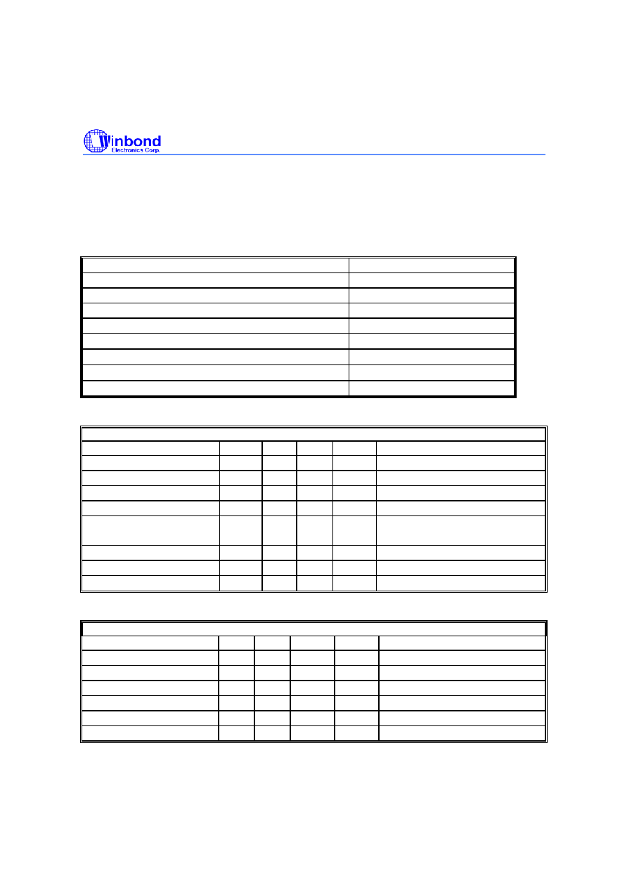
9. SPECIFICATIONS
9.1 Absolute Maximum Ratings
Stresses greater than those listed in this table may cause permanent damage to the device.
Precautions should be taken to avoid application of any voltage higher than the maximum rated
voltages to this circuit. Subjection to maximum conditions for extended periods may affect reliability.
Unused inputs must always be tied to an appropriate logic voltage level (Ground or VDD).
PARAMETER RATING
Absolute 3.3V Core Supply Voltage
-0.5V to +4.6V
Absolute 3.3V I/O Supple Voltage
- 0.5 V to + 4.6 V
Operating 3.3V Core Supply Voltage
3.135V to 3.465V
Operating 3.3V I/O Supple Voltage
3.135V to 3.465V
Storage Temperature
- 65
�
C to + 150
�
C
Ambient Temperature
- 55
�
C to + 125
�
C
Operating Temperature
0
�
C to + 70
�
C
Input ESD protection (Human body model)
2000V
9.2 General Operating Characteristics
VDD48=VDDAGP=VDDREF=VDDPCI= 3.3V
�
5 %, TA = 0
�
C to +70
�
C, Cl=10pF
PARAMETER SYM.
MIN.
MAX.
UNITS
TEST
CONDITIONS
Input Low Voltage
V
IL
0.8 V
dc
Input High Voltage
V
IH
2.0 V
dc
Output Low Voltage
V
OL
0.4 V
dc
All outputs using 3.3V power
Output High Voltage
V
OH
2.4 V
dc
All outputs using 3.3V power
Operating Supply Current
I
dd
350 mA
CPU = 100 to 200 MHz
PCI = 33.3 Mhz with load
Input pin capacitance
Cin
5
pF
Output pin capacitance
Cout
6
pF
Input pin inductance
Lin
7
nH
9.3 Skew Group Timing Clock
VDD48=VDDAGP=VDDREF=VDDPCI = 3.3V
�
5 %, TA = 0
�
C to +70
�
C, Cl=10pF
PARAMETER MIN.
TYP.
MAX.
UNITS
TEST
CONDITIONS
AGP to PCI Skew
1.5
2.6
3.5
ns
Measured at 1.5V
CPU to CPU Skew
200 ps
Crossing
point
AGP to AGP Skew
250 ps
Measured
at
1.5V
PCI to PCI Skew
500 ps
Measured
at
1.5V
48MHz to 48MHz Skew
1000
ps
Measured
at
1.5V
REF to REF Skew
500
ps
Measured at 1.5V

W83194BR-372
- 16 -
9.4 CPU (Open Drain) Electrical Characteristics
VDDCPU= 2.5V
�
5 %, TA = 0
�
C to +70
�
C, external 1.5V pull-up
PARAMETER MIN.
MAX.
UNITS
TEST
CONDITIONS
Rise Time
-
900
ps
100 to 200 Mhz, Vol=20%, Voh=80%
Fall Time
-
900
ps
100 to 200Mhz, Vol=20%, Voh=80%
Absolute crossing point
Voltages
550
1250
mV
100 to 200Mhz
Cycle to Cycle jitter
250
ps
100 to 200Mhz
Duty Cycle
45
55
%
100 to 200Mhz
9.5 AGP, ZCLK
Electrical Characteristics
VDDAGP=VDDZ= 3.3V
�
5 %, TA = 0
�
C to +70
�
C, Test load, Cl=10pF,
PARAMETER MIN.
MAX.
UNITS
TEST
CONDITIONS
Rise Time
500
2000
ps
Measure from 0.4V to 2.4V
Fall Time
500
2000
ps
Measure from 2.4V to 0.4V
Cycle to Cycle jitter
250
ps
Measure 1.5V point
Duty Cycle
45 55 %
Pull-Up Current Min
-33
mA
Vout=1.0V
Pull-Up Current Max
-33
mA
Vout=3.135V
Pull-Down Current Min
30
mA
Vout=1.95V
Pull-Down Current Max
38
mA
Vout=0.4V
9.6 PCI Electrical Characteristics
VDDPCI= 3.3V
�
5 %, TA = 0
�
C to +70
�
C, Test load, Cl=10pF,
PARAMETER MIN.
MAX.
UNITS
TEST
CONDITIONS
Rise Time
500
2000
ps
Measure from 0.4V to 2.4V
Fall Time
500
2000
ps
Measure from 2.4V to 0.4V
Cycle to Cycle jitter
250
ps
Measure 1.5V point
Duty Cycle
45 55 %
Pull-Up Current Min
-33
mA
Vout=1.0V
Pull-Up Current Max
-33
mA
Vout=3.135V
Pull-Down Current Min
30
mA
Vout=1.95V
Pull-Down Current Max
38
mA
Vout=0.4V

W83194BR-372
Publication Release Date: April 13, 2005
- 17 - Revision 1.1
9.7 24M, 48M
Electrical Characteristics
VDD48= 3.3V
�
5 %, TA = 0
�
C to +70
�
C, Test load, Cl=10pF,
PARAMETER MIN.
MAX.
UNITS
TEST
CONDITIONS
Rise Time
500
2000
ps
Measure from 0.4V to 2.4V
Fall Time
500
2000
ps
Measure from 2.4V to 0.4V
Long term jitter
500
ps
Measure 1.5V point
Duty Cycle
45 55 %
Pull-Up Current Min
-33
mA
Vout=1.0V
Pull-Up Current Max
-33
mA
Vout=3.135V
Pull-Down Current Min
30
mA
Vout=1.95V
Pull-Down Current Max
38
mA
Vout=0.4V
9.8 REF Electrical Characteristics
VDDREF= 3.3V
�
5 %, TA = 0
�
C to +70
�
C, Test load, Cl=10pF,
PARAMETER MIN.
MAX.
UNITS
TEST
CONDITIONS
Rise Time
1000
4000
ps
Measure from 0.4V to 2.4V
Fall Time
1000
4000
ps
Measure from 2.4V to 0.4V
Cycle to Cycle jitter
1000
ps
Measure 1.5V point
Duty Cycle
45 55 %
Pull-Up Current Min
-33
mA
Vout=1.0V
Pull-Up Current Max
-33
mA
Vout=3.135V
Pull-Down Current Min
30
mA
Vout=1.95V
Pull-Down Current Max
38
mA
Vout=0.4V
9.9 IOAPIC
Electrical Characteristics
VDDI= 2.5V
�
5 %, TA = 0
�
C to +70
�
C, Test load, Cl=10pF,
PARAMETER MIN.
MAX.
UNITS
TEST
CONDITIONS
Rise Time
400
1600
ps
Measure from 0.4V to 2.0V
Fall Time
400
1600
ps
Measure from 2.0V to 0.4V
Cycle to Cycle jitter
500
ps
Measure 1.25V point
Duty Cycle
45 55 %
Pull-Up Current Min
-27
mA
Vout=1.0V
Pull-Up Current Max
-27
mA
Vout=2.375V
Pull-Down Current Min
27
mA
Vout=1.2V
Pull-Down Current Max
30
mA
Vout=0.3V

W83194BR-372
- 18 -
10. ORDERING INFORMATION
PART NUMBER
PACKAGE TYPE
PRODUCTION FLOW
W83194BR-372
48 PIN SSOP
Commercial, 0
�
C to +70
�
C
11. HOW TO READ THE TOP MARKING
1st line: Winbond logo and the type number: W83194BR-372
2nd line: Tracking code 2 8051234
2: wafers manufactured in Winbond FAB 2
8051234: wafer production series lot number
3rd line: Tracking code 342 G
A
A
SA
342: packages made in '2003, week 42
G: assembly house ID; O means OSE, G means GR
A
: Internal use code
A
: IC revision
SA: mask version
All the trademarks of products and companies mentioned in this data sheet belong to their
respective owners.
W83194BR-372
28051234
342G
BA
SA

W83194BR-372
Publication Release Date: April 13, 2005
- 19 - Revision 1.1
12. PACKAGE DRAWING AND DIMENSIONS

W83194BR-372
- 20 -
13. REVISION HISTORY
VERSION DATE
PAGE
DESCRIPTION
All of the versions before 0.50 are for internal
use.
0.5 09/03/03 n.a.
First published preliminary version.
0.6 10/01/03
1, 6, 7, 10, 11,
12, 16, 17
Modify some description, red text.
0.7 12/18/03
18
Correction IC version, correction some
description and default value
0.8 04/27/04 5,
11
Change frequency table `01101'
1.0 12/28/04
Update
on
Web
1.1 4/13/2005
20
Add
disclaimer
Important Notice
Winbond products are not designed, intended, authorized or warranted for use as components
in systems or equipment intended for surgical implantation, atomic energy control
instruments, airplane or spaceship instruments, transportation instruments, traffic signal
instruments, combustion control instruments, or for other applications intended to support or
sustain life. Further more, Winbond products are not intended for applications wherein failure
of Winbond products could result or lead to a situation wherein personal injury, death or
severe property or environmental damage could occur.
Winbond customers using or selling these products for use in such applications do so at their
own risk and agree to fully indemnify Winbond for any damages resulting from such improper
use or sales.
Headquarters
No. 4, Creation Rd. III,
Science-Based Industrial Park,
Hsinchu, Taiwan
TEL: 886-3-5770066
FAX: 886-3-5665577
http://www.winbond.com.tw/
Taipei Office
TEL: 886-2-8177-7168
FAX: 886-2-8751-3579
Winbond Electronics Corporation America
2727 North First Street, San Jose,
CA 95134, U.S.A.
TEL: 1-408-9436666
FAX: 1-408-5441798
Winbond Electronics (H.K.) Ltd.
No. 378 Kwun Tong Rd.,
Kowloon, Hong Kong
FAX: 852-27552064
Unit 9-15, 22F, Millennium City,
TEL: 852-27513100
Please note that all data and specifications are subject to change without notice.
All the trade marks of products and companies mentioned in this data sheet belong to their respective owners.
Winbond Electronics (Shanghai) Ltd.
200336 China
FAX: 86-21-62365998
27F, 2299 Yan An W. Rd. Shanghai,
TEL: 86-21-62365999
Winbond Electronics Corporation Japan
Shinyokohama Kohoku-ku,
Yokohama, 222-0033
FAX: 81-45-4781800
7F Daini-ueno BLDG, 3-7-18
TEL: 81-45-4781881
9F, No.480, Rueiguang Rd.,
Neihu District, Taipei, 114,
Taiwan, R.O.C.