
W83194BR-KX
STEP-LESS 3-DIMM K7 CLOCK
Publication Release Date: May 2000
- 1 - Revision 0.42
1.0 GENERAL DESCRIPTION
The W83194BR-KX is a Clock Synthesizer which provides all clocks required for AMD K7.
W83194BR-KX provides 64 CPU/PCI frequencies which are selectable with smooth transitions by
hardware or software. W83194BR-KX also provides 13 SDRAM clocks controlled by the none-delay
buffer_in pin.
The W83194BR-KX provides step-less frequency programming by controlling the VCO freq. and the
programmable PCI clock output divisor ratio. A watchdog timer is quipped and when time out, the
RESET# pin will output 4ms pulse signal.
The W83194BR-KX accepts a 14.318 MHz reference crystal as its input. Spread spectrum built in at
±0.5% or ±0.25% to reduce EMI. Programmable stopping individual clock outputs and frequency
selection through I
2
C interface. The device meets the Pentium power-up stabilization, which requires
CPU and PCI clocks be stable within 2 ms after power-up. Using dual function pin for the slots (ISA,
PCI, CPU, DIMM) is not recommend.
2.0 PRODUCT FEATURES
∑
Supports AMD CPU with I
2
C.
∑
3 CPU clocks (one free-running chipset clock controlled by I2C)
∑
13 SDRAM clocks for 3 DIMMs
∑
6 PCI synchronous clocks
∑
One IOAPIC clock for multiprocessor support
∑
Optional single or mixed supply:
(Vddq1=Vddq2 = Vddq3 = Vddq4 = VddL1 =VddL2= 3.3V) or (Vddq1= Vddq2 = Vddq3=Vddq4 =
3.3V, VddL1 = VdqL2 = 2.5V)
∑
< 250ps skew among CPU and SDRAM clocks
∑
< 250ps skew among PCI clocks
∑
< 5ns propagation delay SDRAM from buffer input
∑
Skew from CPU (earlier) to PCI clock 1 to 4ns, center 2.6ns.
∑
Smooth frequency switch with selections from 66 MHz to 200 MHz CPU
∑
Stepless frequency programming by controlling the VCO freq. and the clock output divisor ratio
∑
Programmable skew and driving strength for CPU and SDRAM clock outputs
∑
I
2
C 2-Wire serial interface and I
2
C read back
∑
±0.25% or ±0.5% spread spectrum function to reduce EMI
∑
Programmable registers to enable/stop each output and select modes
∑
MODE pin for power Management and RESET# out when system hang
∑
One 48 MHz for USB & one 24 MHz for super I/O
∑
48-pin SSOP package
W83194BR-KX
PRELIMINARY
Publication Release Date: May 2000
- 2 - Revision 0.42
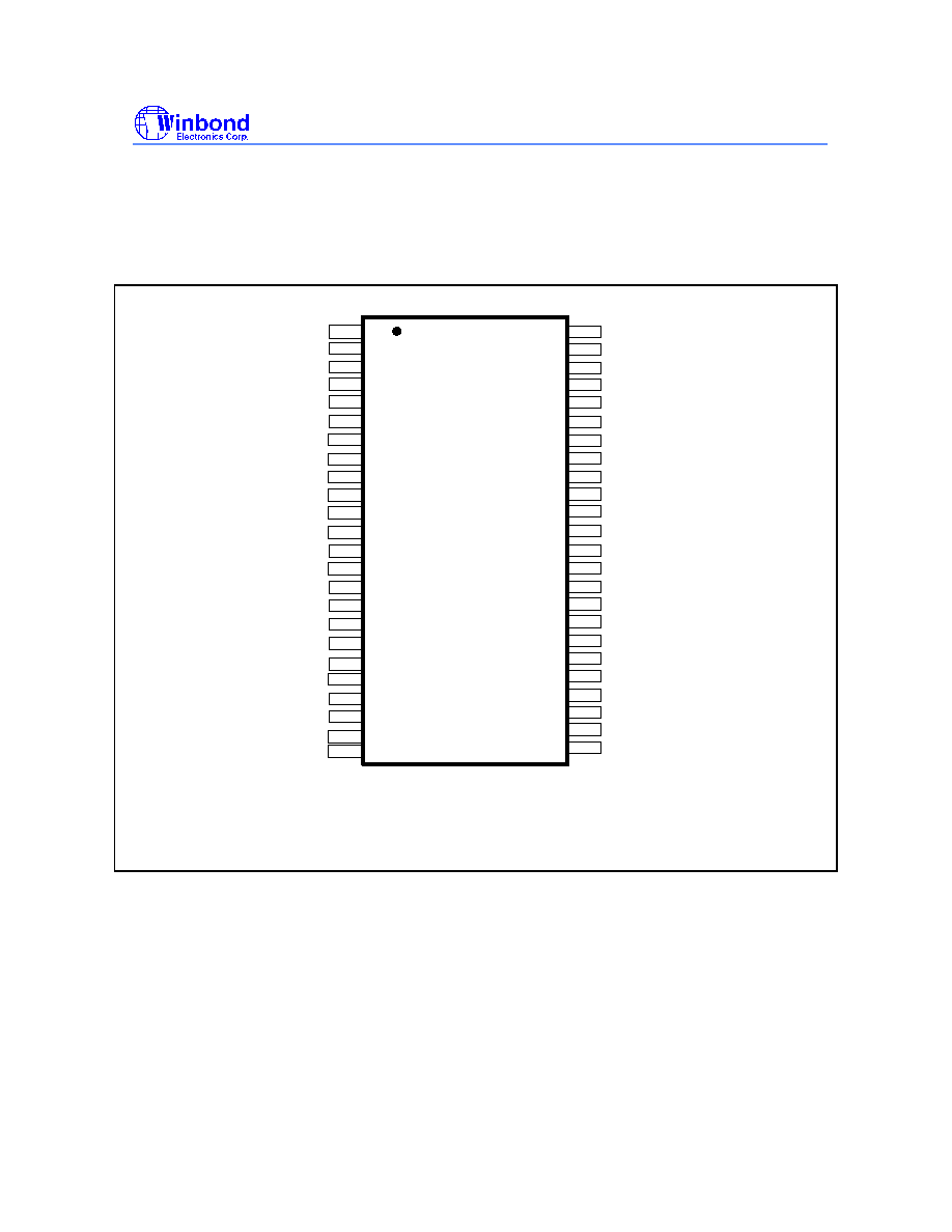
3.0 PIN CONFIGURATION
48
47
46
45
44
43
42
41
40
39
38
37
36
35
34
33
32
31
30
29
28
27
26
25
1
2
3
4
5
6
7
8
9
10
11
12
13
14
15
16
17
18
19
20
21
22
23
24
Vddq3
REF0/FS4*
Vss
Xin
Xout
Vddq3
PCICLK0^/MODE1*
PCICLK1^ /FS1*
Vss
PCICLK2^
PCICLK3^
PCICLK4^
PCICLK5/RESET#
Vddq3
BUFFER IN
Vss
SDRAM11
SDRAM10
Vddq3
SDRAM 9
SDRAM 8
Vss
SDATA*
SDCLK*
REF1/FS0*
Vss
CPUT_CS
CPUC0
VddQ2
PD*#
SDRAM12
Vss
SDRAM 0
SDRAM 1
SDRAM 2
Vddq3
SDRAM 3
Vss
SDRAM 4
SDRAM 5
SDRAM 6
SDRAM 7
Vddq3
Vddq3
48MHz/FS2*
24_48MHz/FS3*
CPUT0
Vss
* : Internal pull-up
^ : 1.5X~2X driving strength
$ : Internal pull-low
4.0 PIN DESCRIPTION
IN - Input
OUT - Output
I/O - Bi-directional Pin
# - Active Low
* - Internal 250k
pull-up
W83194BR-KX
PRELIMINARY
Publication Release Date: May 2000
- 3 - Revision 0.42
4.1 Crystal I/O
SYMBOL
PIN
I/O
FUNCTION
Xin
4
IN Crystal input with internal loading capacitors and
feedback resistors.
Xout
5
OUT Crystal output at 14.318MHz nominally.
4.2 CPU, SDRAM, PCI, IOAPIC Clock Outputs
SYMBOL
PIN
I/O
FUNCTION
CPUT_CS
CPU_C0
CPU_T0
46
44
43
OD CPU_C0 and CPU_T0 are the differential open drain
CPU clocks for K7. CPUT_CS is the open drain pin
for the chipset. It has the same phase relationship as
CPU_T0.
SDRAM [ 0 :12]
17,18,20,21,28,2
9,31,32,34,
35,37,38,40
OUT SDRAM clock outputs. Fanout buffer outputs from
BUFFER IN pin.(Controlled by chipset) They are
disabled when PD# is set LOW.
PCICLK0/
*MODE1
7
I/O Free running PCI clock during normal operation.
Latched Input. Mode1=1, Pin 13 is PCICLK 5;
*Mode1=0, RESET# open drain. (4ms low active
pulse when Watch Dog time out)
PCICLK1/*FS1
8
I/O Low skew (< 250ps) PCI clock outputs.
Latched input for FS1 at initial power up for H/W
selecting the output frequency of CPU, SDRAM and
PCI clocks.
PCICLK [ 2 : 4 ]
10, 11,12
OUT Low skew (< 250ps) PCI clock outputs. Synchronous
to CPU clocks with 1-48ns skew (CPU early).
PCICLK5/RESET#
13
I/O Low skew (< 250ps) PCI clock outputs.
Mode1=1, Pin 13 is PCICLK5; *Mode1=0, RESET#
open drain. (4ms low active pulse when Watch Dog
time out)
BUFFER IN
15
IN Inputs to fanout for SDRAM outputs.
*PD#
41
IN The all clocks will be stopped when this pin set to
LOW.
W83194BR-KX
PRELIMINARY
Publication Release Date: May 2000
- 4 - Revision 0.42
4.3 I
2
C Control Interface
SYMBOL
PIN
I/O
FUNCTION
*SDATA
23
I/O Serial data of I
2
C 2-wire control interface with internal
pull-up resistor.
*SDCLK
24
IN Serial clock of I
2
C 2-wire control interface with
internal pull-up resistor.
4.4 Fixed Frequency Outputs
SYMBOL
PIN
I/O
FUNCTION
REF0/ *FS4
2
I/O 14.318MHz reference clock.
Latched input for FS4 at initial power up for H/W
selecting the output frequency of CPU, SDRAM and
PCI clocks
REF1 / *FS0
48
I/O 14.318MHz reference clock.
Latched input for FS0 at initial power up for H/W
selecting the output frequency of CPU, SDRAM and
PCI clocks.
24_48MHz / *FS3
25
I/O 24MHz output clock.
Latched input for FS3 at initial power up for H/W
selecting the output frequency of CPU, SDRAM and
PCI clocks.
48MHz / *FS2
26
I/O 48MHz output for USB during normal operation.
Latched input for FS2 at initial power up for H/W
selecting the output frequency of CPU, SDRAM and
PCI clocks.
4.5 Power Pins
SYMBOL
PIN
FUNCTION
Vddq2
42
Power supply for CPU clocks, 2.5V or 3.3V.
Vddq3
1,6,14,19,27,30,36 Power supply for PCI, 24_48MHz, SDRAM [0:12], and
CPU PLL core, nominal 3.3V.
Vss
3,9,16,22,33,39,45,
47
Circuit Ground.
W83194BR-KX
PRELIMINARY
Publication Release Date: May 2000
- 5 - Revision 0.42
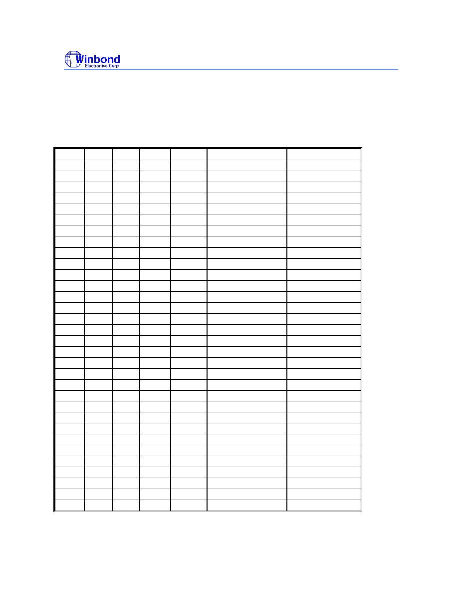
5.0 FREQUENCY SELECTION
5.1 H/W Setting Frequency Table
FS4
FS3
FS2
FS1
FS0
CPU (MHz)
PCI (MHz)
0
0
0
0
0
166.00
41.60
0
0
0
0
1
160.00
40.00
0
0
0
1
0
155.00
38.70
0
0
0
1
1
150.00
37.50
0
0
1
0
0
145.00
36.20
0
0
1
0
1
140.00
35.00
0
0
1
1
0
136.00
34.00
0
0
1
1
1
130.00
32.50
0
1
0
0
0
127.00
31.70
0
1
0
0
1
124.00
31.00
0
1
0
1
0
120.00
40.00
0
1
0
1
1
118.00
39.30
0
1
1
0
0
116.00
38.60
0
1
1
0
1
115.00
38.30
0
1
1
1
0
114.00
38.00
0
1
1
1
1
113.00
37.60
1
0
0
0
0
112.00
37.30
1
0
0
0
1
111.00
37.00
1
0
0
1
0
110.00
36.60
1
0
0
1
1
109.00
36.30
1
0
1
0
0
108.00
36.00
1
0
1
0
1
107.00
35.60
1
0
1
1
0
106.00
35.30
1
0
1
1
1
104.00
34.60
1
1
0
0
0
102.00
34.00
1
1
0
0
1
133.60
33.40
1
1
0
1
0
133.90
33.40
1
1
0
1
1
133.30
33.30
1
1
1
0
0
95.00
31.70
1
1
1
0
1
100.30
33.30
1
1
1
1
0
100.90
33.40
1
1
1
1
1
100.60
33.30