
W83194BR-P4X
STEPLESS VIA P4X/P4M MAIN
CLOCK GENERATOR
Date: 02/21/2003 Revision: 2.0
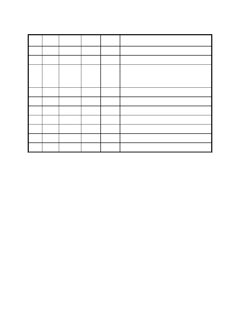
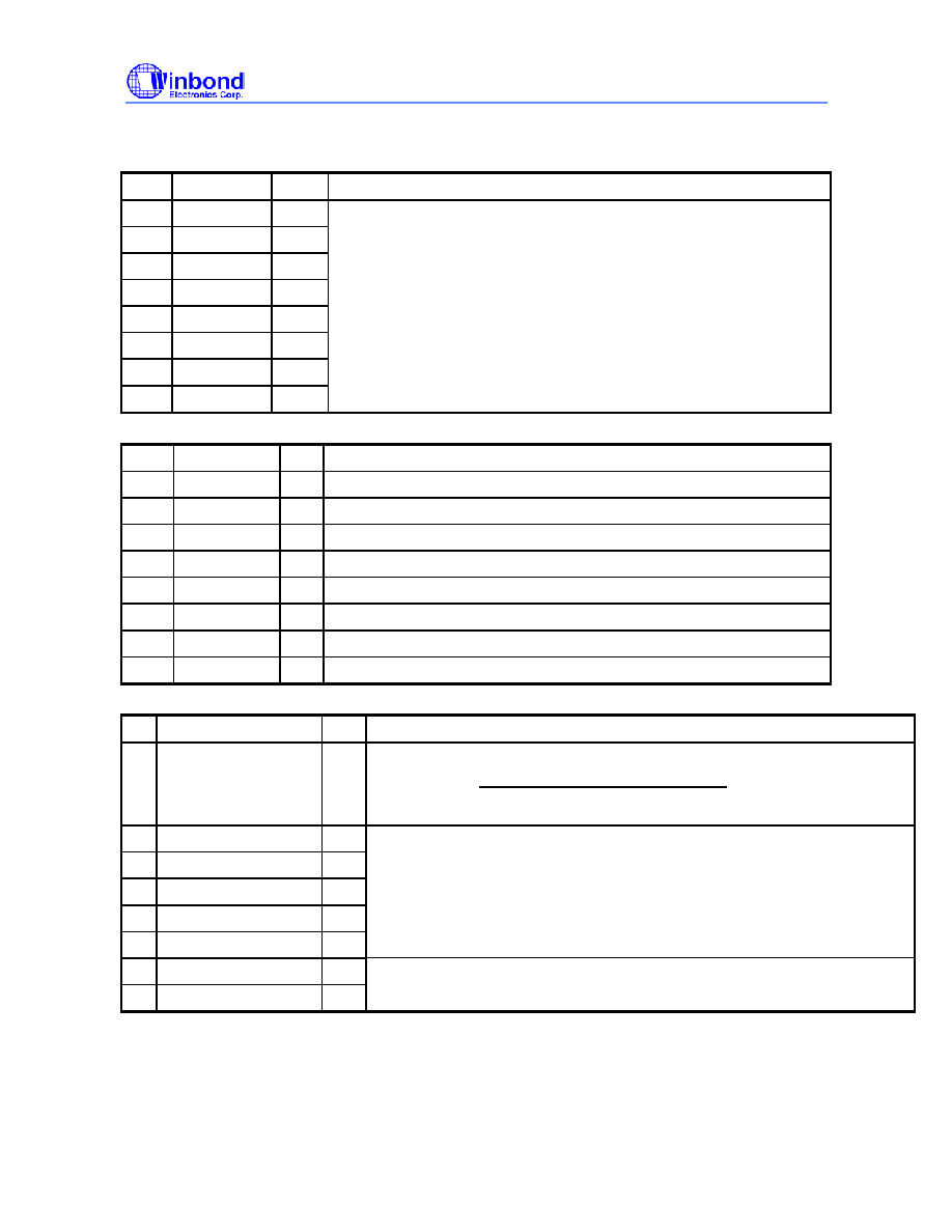
W83194BR-P4X Data Sheet Revision History
NO. Pages Dates Version Web
Version
Main Contents
1
n.a.
n.a.
All of the versions before 0.50 are for internal use.
2
n.a. 7/01/2002 1.0
n.a Change
version
and version on web site to 1.0
3
4,10
8/07/2002
1.1
1.1
FS1 internal 120K pull up change to pull down.
Register 3: bit 0,1 PCISTOPB read back &
CPUSTOPB read back exchange.
Change version and version on web site to 1.1
4
5 9/19/2002 1.2 1.2 VTTPWGD#
This pin is LOW active.
5
All
2/21/2003
2.0
2.0
Update new form
6
7
8
9
10
Please note that all data and specifications are subject to change without notice. All
the trademarks of products and companies mentioned in this data sheet belong to
their respective owners.
LIFE SUPPORT APPLICATIONS
These products are not designed for use in life support appliances, devices, or
systems where malfunction of these products can reasonably be expected to result
in personal injury. Winbond customers using or selling these products for use in such
applications do so at their own risk and agree to fully indemnify Winbond for any
damages resulting from such improper use or sales.

STEPLESS CLOCK FOR VIA P4 CHIPSET
Publication Release Date: February 2003
- I -
Revision 2.0
W83194BR-P4X
TABLE OF CONTENT
1. GENERAL DESCRIPTION ..................................................................................... 1
2. PRODUCT FEATURES .......................................................................................... 1
3. BLOCK DIAGRAM ................................................................................................. 2
4. PIN CONFIGURATION........................................................................................... 2
5. PIN DESCRIPTION................................................................................................. 3
5.1 CRYSTAL I/O ........................................................................................................................................3
5.2 CPU, AGP, AND PCI, IOAPIC CLOCK OUTPUTS.............................................................................3
5.3 I
2
C CONTROL INTERFACE.................................................................................................................4
5.4 FIXED FREQUENCY OUTPUTS.........................................................................................................4
5.5 POWER MANAGEMENT PINS............................................................................................................4
5.6 POWER PINS........................................................................................................................................5
5.7 HARDWARE MULTSEL [1:0] SELECTS FUNCTION.........................................................................5
6. FREQUENCY SELECTION BY HARDWARE OR SOFTWARE ............................ 6
7. I
2
C CONTROL AND STATUS REGISTERS........................................................... 7
7.1 REGISTER 0: FREQUENCY SELECT REGISTER (DEFAULT = 0) .................................................7
7.2 REGISTER 1: CPU CLOCK REGISTER (1 = ENABLE, 0 = STOPPED) ..........................................7
7.3 REGISTER 2: PCI CLOCK REGISTER (1 = ENABLE, 0 = STOPPED) ............................................7
7.4 REGISTER 3: PCI, REF, 48MHZ CLOCK REGISTER (1 = ENABLE, 0 = STOPPED) ....................8
7.5 REGISTER 4:MULTISEL1 IOAPIC, AGP CONTROL REGISTER (1 = ENABLE, 0 = STOPPED)..8
7.6 REGISTER 5: WATCHDOG CONTROL REGISTER .........................................................................9
7.7 THE REGISTER 6, 7 IS RESERVED FOR BUFFER..........................................................................9
7.8 REGISTER 8: WATCHDOG TIMER REGISTER ................................................................................9
7.9 REGISTER 9: M/N PROGRAM REGISTER........................................................................................9
7.10 REGISTER 10: M/N PROGRAM REGISTER..................................................................................10
7.11 REGISTER 11: SPREAD SPECTRUM PROGRAMMING REGISTER .........................................10
7.12 REGISTER 12: DIVISOR AND STEP-LESS ENABLE CONTROL REGISTER............................10
7.13 REGISTER 13: CPU TO IOAPIC SKEW CONTROL......................................................................12
7.14 REGISTER 14: CPU TO PCI AND IOAPIC SKEW CONTROL......................................................12
7.15 REGISTER 15: SEL24_48 AND CPU TO CPUCS SKEW CONTROL..........................................12
7.16 REGISTER 16: RESERVED ............................................................................................................13
7.17 REGISTER 17: RESERVED ............................................................................................................13
7.18 REGISTER 18: RESERVED ............................................................................................................13
7.19 REGISTER 19: WINBOND CHIP ID REGISTER (READ ONLY)................................................14
7.20 REGISTER 20: WINBOND CHIP ID REGISTER (READ ONLY)................................................14
8.ACCESS INTERFACE........................................................................................... 15

STEPLESS CLOCK FOR VIA P4 CHIPSET
Publication Release Date: February 2003
- II -
Revision 2.0
W83194BR-P4X
8.1 BLOCK WRITE PROTOCOL..............................................................................................................15
8.2 BLOCK READ PROTOCOL ...............................................................................................................15
8.3 BYTE WRITE PROTOCOL.................................................................................................................15
8.4 BYTE READ PROTOCOL ..................................................................................................................15
9. SPECIFICATIONS ................................................................................................ 16
9.1 ABSOLUTE MAXIMUM RATINGS.....................................................................................................16
10. ORDERING INFORMATION............................................................................... 16
11. HOW TO READ THE TOP MARKING................................................................ 16
12. PACKAGE DRAWING AND DIMENSIONS ....................................................... 17

STEPLESS CLOCK FOR VIA P4 CHIPSET
Publication Release Date: February 2003
- 1 - Revision 2.0
W83194BR-P4X
1. GENERAL DESCRIPTION
The W83194BR-P4X is a Clock Synthesizer for VIA P4 chipset. W83194BR-P4X provides all clocks
required for high-speed microprocessor and provides step-less frequency programming and 32
different frequencies of CPU, PCI, and AGP clocks setting. All clocks are externally selectable with
smooth transitions.
The W83194BR-P4X provides I
2
C serial bus interface to program the registers to enable or disable
each clock outputs and provides -0.5% and +/-0.25% center type spread spectrum or programmable
S.S.T. scale to reduce EMI.
The W83194BR-P4X also has watch dog timer and reset output pin to support auto-reset when
systems hanging caused by improper frequency setting.
The W83194BR-P4X accepts a 14.318 MHz reference crystal as its input and runs on a 3.3V supply.
High drive PCI CLOCK outputs typically provide greater than 1 V /ns slew rate into 30 pF loads. The
fixed frequency outputs as REF and 48 MHz provide better than 0.5V /ns slew rate.
2. PRODUCT FEATURES
� 2 Differential pairs of CPU clock outputs
� 1 Differential pairs push pull of CPU_CS clock outputs
� 3 AGP clock outputs
� 9 PCI synchronous clocks
� 24_48Mhz clock output for super I/O.
� 48 MHz clock output for USB.
� 2 IOAPIC clock outputs.
� 1 REF clock output.
� Skew form CPU to PCI clock 1 to 4 ns, center 2.6 ns
� Smooth frequency switch with selections from 66.8 to 200MHz
� Step-less frequency programming
� I
2
C 2-Wire serial interface and support byte read/write and block read/write.
� -0.5% and +/- 0.25% center type spread spectrum
� Programmable S.S.T. scale to reduce EMI
� Programmable registers to enable/stop each output and select modes
� Watch Dog Timer and RESET# output pins
� 48-pin SSOP package
STEPLESS CLOCK FOR VIA P4 CHIPSET
Publication Release Date: February 2003
- 2 - Revision 2.0
W83194BR-P4X
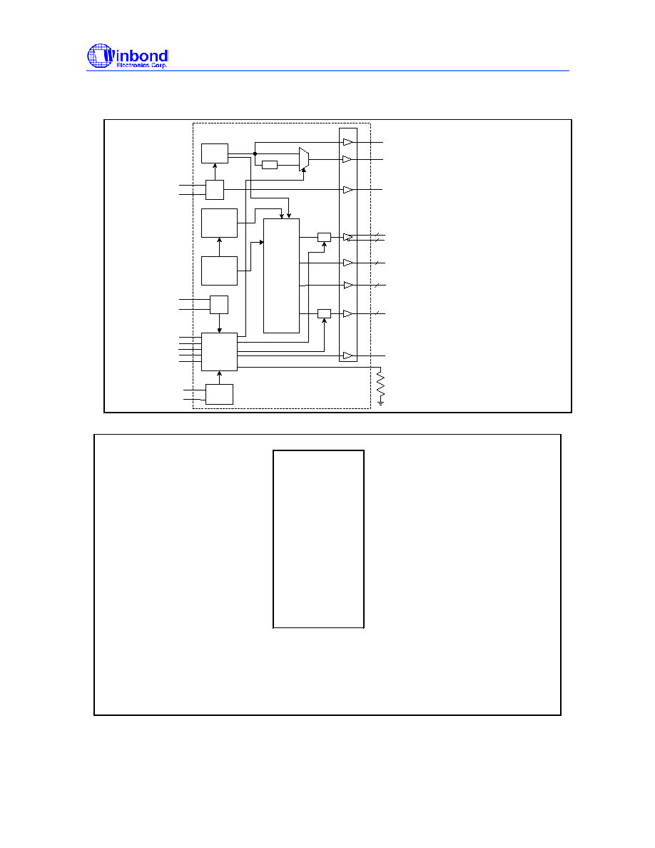
3. BLOCK DIAGRAM
PLL2
Mux
Control
Logic
&
Config
Register
Divider
/2,/4,/8,/16
/3,/6,/12
/5,/10,/20
/7,/14
/9,/18
1/2
Stop
XTAL
OSC
PLL1
Spread
Spectrum
Stop
M/N/Ratio
S.S.P
ROM
Driver
VCOCLK
48MHz
24_48MHz
REF
CPUCLK_T 0:1, CS
CPUCLK_C 0:1, CS
AGP 0:2
PCICLK_F
PCICLK_0:7
RESET#
Rref
XIN
XOUT
SDATA*
SDCLK*
FS<4:0>
PD#*
CPU_STOP#*
PCI_STOP#*
MULTISEL0*
VTTPWRGD#
Latch
&
POR
I2C
interface
9
3
3
3
IOAPIC 0:1
2
SEL24_48&
4. PIN CONFIGURATION
S E L 2 4 _ 4 8 & / R E F 1
4 8 V D D A P I C ( 2 . 5 V )
V D D R E F 2
4 7 G N D
G N D 3
4 6 I O A P I C 0
X I N 4
4 5 I O A P I C 1
X O U T 5
4 4 G N D
V D D 4 8 6
4 3 V D D C P U ( 2 . 5 V )
F S 3 & / 4 8 M H z 7
4 2 C P U C L K T _ C S
F S 2 & / 2 4 _ 4 8 M H z 8
4 1 C P U C L K C _ C S
G N D 9
4 0 C P U C L K _ T 0
F S 0 * / P C I C L K _ F 1 0
3 9 C P U C L K _ C 0
F S 1 & / P C I C L K 0 1 1
3 8 V D D C P U ( 3 . 3 V )
M U L T I S E L 0 * / P C I C L K 1 1 2
3 7 I R E F
G N D 1 3
3 6 G N D
P C I C L K 2 1 4
3 5 C P U C L K _ T 1
P C I C L K 3 1 5
3 4 C P U C L K _ C 1
V D D P C I 1 6
3 3 V T T P W R G #
P C I C L K 4 1 7
3 2 C P U _ S T O P # *
P C I C L K 5 1 8
3 1 P C I _ S T O P # *
P C I C L K 6 1 9
3 0 R E S E T #
G N D 2 0
2 9 S D A T A *
P C I C L K 7 2 1
2 8 S D C L K *
P D # * 2 2
2 7 A G P 2
A G P 0 2 3
2 6 A G P 1
V D D A G P 2 4
2 5 G N D
#: Active low
^: These outputs have 1.5 ~ 2X drive strength
*: Internal pull up resistor 120K to VDD
&: Internal Pull-down resistor 120K to GND

STEPLESS CLOCK FOR VIA P4 CHIPSET
Publication Release Date: February 2003
- 3 - Revision 2.0
W83194BR-P4X
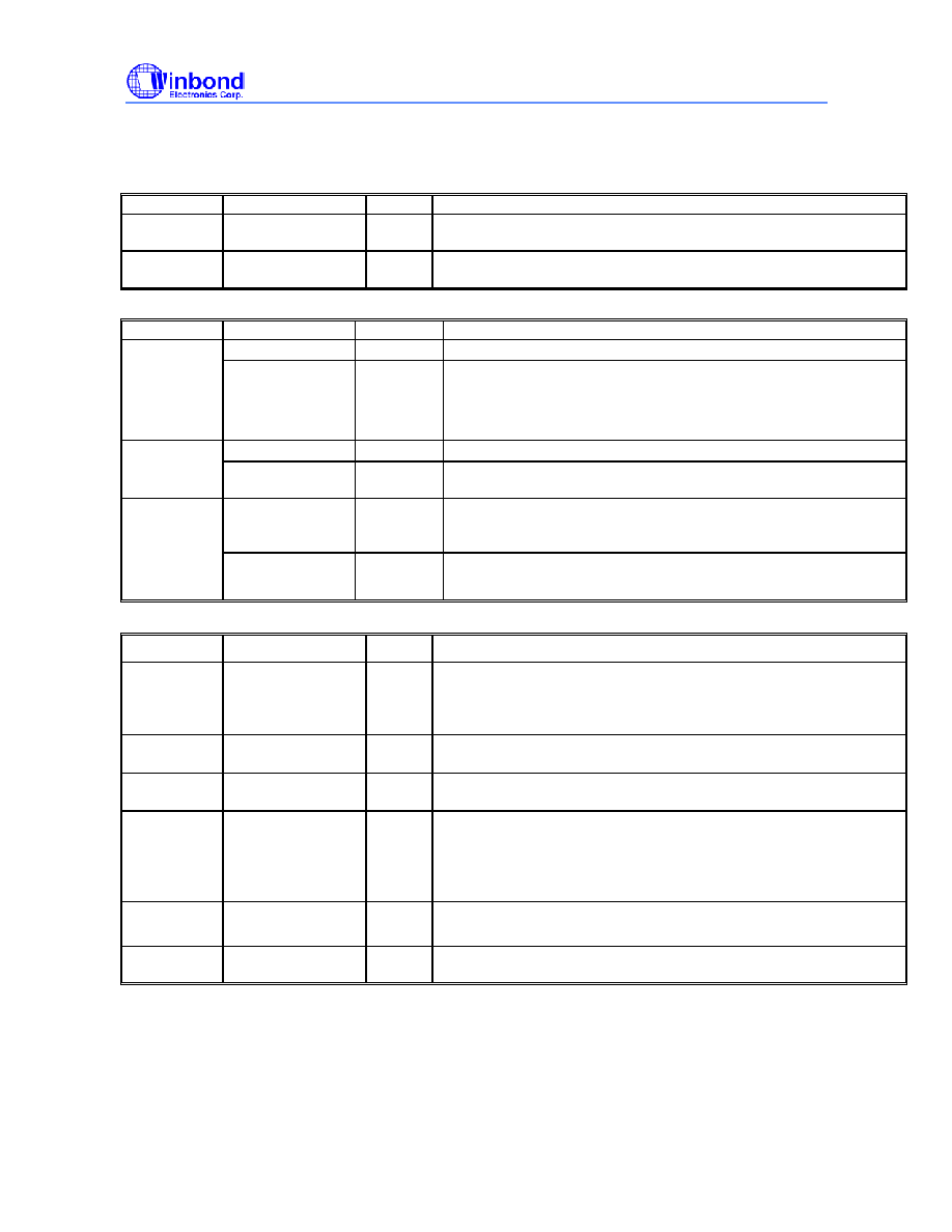
5. PIN DESCRIPTION
Buffer type symbol
Description
IN Input
IN
tp120k
Latched input at power up, internal 120k pull up.
IN
td120k
Latched input at power up, internal 120k pull down.
OUT Output
OD Open
Drain
I/O Bi-directional
Pin
I/OD
Bi-directional Pin, Open Drain.
# Active
Low
*
Internal 120k
pull-up
&
Internal 120 k
pull-down
5.1 Crystal I/O
PIN Pin
Name
Type Description
4 XIN
IN
Crystal input with internal loading capacitors (18pF) and feedback
resistors.
5 XOUT
OUT Crystal output at 14.318MHz nominally with internal loading
capacitors (18pF).
5.2 CPU, AGP, and PCI, IOAPIC Clock Outputs
PIN Pin
Name
Type Description
34,35,39,40
CPUCLK_T [0:1]
CPUCLK_C [0:1]
OUT Low skew (< 250ps) differential clock outputs for host frequencies of
CPU
41,42
CPUCLKT_CS
CPUCLKC_CS
OUT Low skew (< 250ps) differential push pull clock outputs for host
frequencies of CHIPSET
23,26,27 AGP0:
2 OUT 3.3V AGP clock outputs.
PCICLK_F
OUT 3.3V free running PCI clock output.
10
FS0*
IN
tp120k
Latched input for FS0 at initial power up for H/W selecting the
output frequency. This is internal 120K pull up.
PCICLK0
OUT 3.3V PCI clock output.
11
FS1&
IN
td120k
Latched input for FS1 at initial power up for H/W selecting the
output frequency, This is internal 120K pull down.
PCICLK1
OUT 3.3V PCI clock output.
12
MULTI_SEL0*
IN
tp120k
Latched input for MULTSEL0 at initial power up, internal 120K pull
up
14,15,17,18,
19,21
PCICLK [2:7]
OUT Low skew (< 250ps) PCI clock outputs.
45,46 IOAPIC0:
1
OUT 2.5V PCI/2 clock outputs.
STEPLESS CLOCK FOR VIA P4 CHIPSET
Publication Release Date: February 2003
- 4 - Revision 2.0
W83194BR-P4X
5.3 I
2
C Control Interface
PIN Pin
Name
Type
Description
25 SDATA*
I/OD Serial data of I
2
C 2-wire control interface with internal pull-up
resistor.
26 SDCLK*
IN
Serial clock of I
2
C 2-wire control interface with internal pull-up
resistor.
5.4 Fixed Frequency Outputs
PIN Pin
Name
Type
Description
REF
OUT 14.318MHz
output.
1
SEL24_48&
IN
td120k
Latched input for 24MHz or 48MHz select pin. This is internal
120K pull down default 24MHz. In power on reset period, it is a
hardware-latched pin, and it can be R/W by I2C control after
power on reset period. Select by register 16 bit 6.
48MHz
OUT
48MHz clock output for USB.
7
FS3&
IN
td120k
Latched input for FS3 at initial power up for H/W selecting the
output frequency. This is internal 120K pull down.
24_48MHz
OUT
24(default) or 48MHz clock output, In power on reset period, it is a
hardware-latched pin, and it can be R/W by I2C control after
power on reset period. Select by register 16 bit 7.
8
FS2&
IN
td120k
Latched input for FS2 at initial power up for H/W selecting the
output frequency. This is internal 120K pull down.
5.5 Power Management Pins
PIN Pin
Name
Type Description
33 VTTPWGD#
IN
Power good input signal comes from ACPI with LOW active. This
3.3V input is level sensitive strobe used to determine FS [4:0] and
MULTISEL input are valid and is ready to sample. This pin is LOW
active.
32 CPU_STOP#*
IN
CPU clock stop control pin, This pin is low active. Internal 120k
pull-up.
31 PCI_STOP#*
IN
PCI clock stop control pin, This pin is low active. Internal 120k
pull-up.
37 IREF
IN
Deciding the reference current for the CPUCLK pairs. The pin was
connected to the precision resistor tied to ground to decide the
appropriate current. There are several modes to select different
current via power on trapping the Pin 12 (MULTISEL). The table is
show as follows.
30 RESET#
OD
System reset signal when the watchdog is time out. This pin will
generate 250ms low phase when the watchdog timer is timeout.
22 PD#*
IN
Power Down Function. This is power down pin, low active (PD#).
Internal 120K pull up
STEPLESS CLOCK FOR VIA P4 CHIPSET
Publication Release Date: February 2003
- 5 - Revision 2.0
W83194BR-P4X
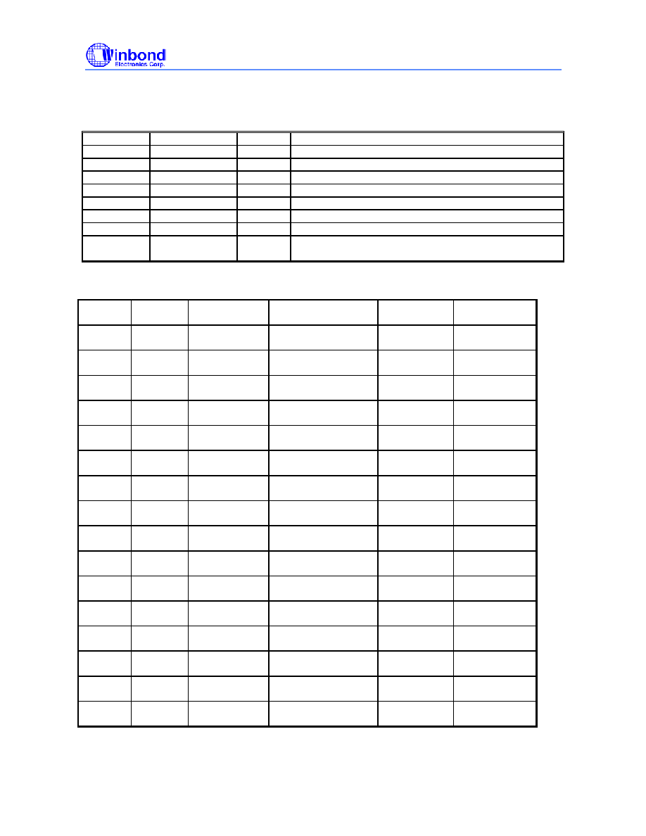
5.6 Power Pins
PIN Pin
Name
Type
Description
2
VDDREF
PWR
3.3V power supply for REF.
16
VDDPCI
PWR
3.3V power supply for PCI.
24
VDDAGP
PWR
3.3V power supply for AGP.
38
VDDCPU
PWR
3.3V power supply for CPU.
43
VDDCPU_CS
PWR
2.5V power supply for CPUCLKT & C _CS.
48
VDDAPIC
PWR
2.5V power supply for IOAPIC.
6
VDD48
PWR
Analog power 3.3V for 48MHz.
3,9,13,20,25,
36,44,47
GND PWR
Ground pin for 3.3 V
5.7 Hardware MULTSEL [1:0] selects Function
Multsel1 Multsel0 Board
Target
trace/Term Z
Reference R, IREF
= Add/(3*Rr)
Output
Current
Voh @ Z
0 0 50
Rr =221 1%
IREF = 5.00mA
Ioh=4*IREF
1.0V @ 50
0 0 60
Rr =221 1%
IREF = 5.00mA
Ioh=4*IREF
1.2V @ 60
0 1 50
Rr =221 1%
IREF = 5.00mA
Ioh=5*IREF
1.25V @ 50
0 1 60
Rr =221 1%
IREF = 5.00mA
Ioh=5*IREF
1.5V @ 60
1 0 50
Rr =221 1%
IREF = 5.00mA
Ioh=6*IREF
1.5V @ 50
1 0 60
Rr =221 1%
IREF = 5.00mA
Ioh=6*IREF
1.8V @ 60
1 1 50
Rr =221 1%
IREF = 5.00mA
Ioh=7*IREF
1.75V @ 50
1 1 60
Rr =221 1%
IREF = 5.00mA
Ioh=7*IREF
2.1V @ 50
0 0 50
Rr =475 1%
IREF = 2.32mA
Ioh=4*IREF
0.47V @ 50
0 0 60
Rr =475 1%
IREF = 2.32mA
Ioh=4*IREF
0.56V @ 50
0 1 50
Rr =475 1%
IREF = 2.32mA
Ioh=5*IREF
0.58V @ 50
0 1 60
Rr =475 1%
IREF = 2.32mA
Ioh=5*IREF
0.7V @ 60
1 0 50
Rr =475 1%
IREF = 2.32mA
Ioh=6*IREF
0.7V @ 50
1 0 60
Rr =475 1%
IREF = 2.32mA
Ioh=6*IREF
0.84V @ 60
1 1 50
Rr =475 1%
IREF = 2.32mA
Ioh=7*IREF
0.81V @ 50
1 0 60
Rr =475 1%
IREF = 2.32mA
Ioh=6*IREF
0.97V @ 60
STEPLESS CLOCK FOR VIA P4 CHIPSET
Publication Release Date: February 2003
- 6 - Revision 2.0
W83194BR-P4X
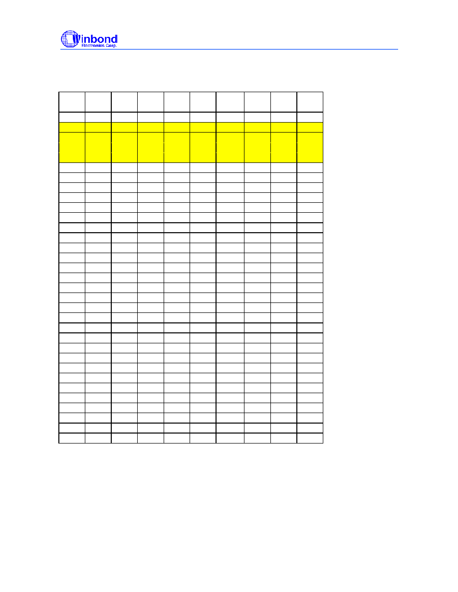
6. FREQUENCY SELECTION BY HARDWARE OR SOFTWARE
This frequency table is used at power on latched FS [4:0] value or software programming at SSEL
[4:0] (Register 0 bit 6 ~ 2).
FS4 FS3 FS2 FS1 FS0 CPU
(MHZ)
AGP
(MHZ) PCI (MHz) IOAPIC (MHz) Spread %
0 0 0 0 0
66.7 66.66 33.33
16.665
+/-0.25%
0 0 0 0 1
100.0 66.67 33.335
16.668
+/-0.25%
0 0 0 1 0
133.3 66.67 33.335
16.668
+/-0.25%
0 0 0 1 1
200.0 66.66 33.33
16.665
+/-0.25%
0 0 1 0 0
100.9 67.27 33.635
16.818
+/-0.25%
0 0 1 0 1
103.0 68.67 34.335
17.168
+/-0.25%
0 0 1 1 0
107.0 71.33 35.665
17.833
+/-0.25%
0 0 1 1 1
110.0 73.33 36.665
18.333
+/-0.25%
0 1 0 0 0
133.9 66.95 33.475
16.738
+/-0.25%
0 1 0 0 1
137.3 68.66 34.33
17.165
+/-0.25%
0 1 0 1 0
140.0
70
35
17.5
+/-0.25%
0 1 0 1 1
142.7 71.33 35.665
17.833
+/-0.25%
0 1 1 0 0
145.3 72.66 36.33
18.165
+/-0.25%
0 1 1 0 1
146.7 73.33 36.665
18.333
+/-0.25%
0 1 1 1 0
153.3 76.66 38.33
19.165
+/-0.25%
0 1 1 1 1
160.0
80
40
20
+/-0.25%
1 0 0 0 0
66.7 66.66 33.33
16.665 -0.5%
1 0 0 0 1
100.0 66.67 33.335
16.668 -0.5%
1 0 0 1 0
133.3 66.67 33.335
16.668 -0.5%
1 0 0 1 1
200.0 66.66 33.33
16.665 -0.5%
1 0 1 0 0
66.7 66.66 33.33
16.665
+/-0.25%
1 0 1 0 1
100.0 66.67 33.335
16.668
+/-0.25%
1 0 1 1 0
133.3 66.67 33.335
16.668
+/-0.25%
1 0 1 1 1
200.0 66.66 33.33
16.665
+/-0.25%
1 1 0 0 0
201.0
67
33.5
16.75
+/-0.25%
1 1 0 0 1
203.0 67.67 33.835
16.918
+/-0.25%
1 1 0 1 0
205.0 68.33 34.165
17.083
+/-0.25%
1 1 0 1 1
207.0
69
34.5
17.25
+/-0.25%
1 1 1 0 0
209.0 69.67 34.835
17.418
+/-0.25%
1 1 1 0 1
211.0 70.33 35.165
17.583
+/-0.25%
1 1 1 1 0
213.0
71
35.5
17.75
+/-0.25%
1 1 1 1 1
215.0 71.67 35.835
17.918
+/-0.25%
STEPLESS CLOCK FOR VIA P4 CHIPSET
Publication Release Date: February 2003
- 7 - Revision 2.0
W83194BR-P4X
7. I
2
C CONTROL AND STATUS REGISTERS
7.1 Register 0: Frequency Select Register (default = 0)
Bit Name
PWD
Description
7 SSEL
[3] 0
6 SSEL
[2] 0
5 SSEL
[1] 0
4 SSEL
[0] 0
Frequency selection by software via I
2
C
3
EN_SSEL
0 Enable software program FS [4:0].
0 = Select frequency by hardware.
1= Select frequency by software I
2
C - Bit 7~ 4,2.
2
SSEL [4]
0
Frequency selection bit 4
1
EN_SPSP
0
Enable Spread Spectrum in the frequency table.
0 = Normal
1 = Spread Spectrum enabled
0
EN_SAFE_FREQ
0
Enable reload safe frequency when the watchdog is timeout.
0 = reload the FS [4:0] latched pins when watchdog time out.
1 = reload the safe frequency bit defined at Register 5 bit 4~0.
7.2 Register 1: CPU Clock Register (1 = enable, 0 = Stopped)
Bit Pin
NO
PWD
Description
7
42,41
1 CPUCLK_T / C_CS
6
35,34
1 CPUCLK_T1 / C1
5
40,39
1 CPUCLK_T0 / C0
4
-
X FS [4] Read back.
3
-
X FS [3] Read back
2
-
X FS [2] Read back
1
-
X FS [1] Read back
0
-
X FS [0] Read back
7.3 Register 2: PCI Clock Register (1 = enable, 0 = Stopped)
Bit Pin
NO
PWD
Description
7 21 1
PCICLK7
6 19 1
PCICLK6
5 18 1
PCICLK5
4 17 1
PCICLK4
3 15 1
PCICLK3
2 14 1
PCICLK2
STEPLESS CLOCK FOR VIA P4 CHIPSET
Publication Release Date: February 2003
- 8 - Revision 2.0
W83194BR-P4X
1 12 1
PCICLK1
0 11 1
PCICLK0
7.4 Register 3: PCI, REF, 48MHz Clock Register (1 = enable, 0 = Stopped)
Bit Pin
NO
PWD
Description
7 7 1
48MHZ
6 8 1
24_48MHz
5 1 1
REF
4 10 1
PCICLK_F
3
41,42
1 CPUCS Stop control: 0: CPUCLK1 free run
1: CPUCLK1 can stopped by CPU_STOP#
2
8
0 PCI_F Stop control 0: PCI_F free run
1: PCI_F can stopped by PCI_STOP#
1
32
1 PCISTOPB read back
0
31
1 CPUSTOPB read back
7.5 Register 4:MULTISEL1 IOAPIC, AGP Control Register (1 = enable, 0 = Stopped)
Bit Pin
NO
PWD
Description
7
-
0 MULTISEL1 I2C R/W
6 - 1
Reserved
5 - 1
Reserved
4 45 1
IOAPIC1
3 46 1
IOAPIC0
2 27 1
AGP2
1 26 1
AGP1
0 23 1
AGP0
STEPLESS CLOCK FOR VIA P4 CHIPSET
Publication Release Date: February 2003
- 9 - Revision 2.0
W83194BR-P4X
7.6 Register 5: Watchdog Control Register
Bit Name
PWD
Description
7
MULTISEL0
X Pin 12 MULTISEL0 power on trapping pin data read back
6 EN_WD
0 Enable Watchdog Timer if set to 1. Set to 0, disable watchdog timer.
Read this bit will return a counting state. If timer continues down count,
this bit will return 1. Otherwise, this bit will return 0.
5 WD_TIMEOUT 0 Watchdog Timeout Status. If the watchdog is started and timer down
counts to zero, this bit will be set to 1. Clear this bit to logic 0, If set to 1,
when the watchdog is restart in the next time. This bit is Read Only.
4 SAF_FREQ
[4] 0
3 SAF_FREQ
[3] 0
2 SAF_FREQ
[2] 0
1 SAF_FREQ
[1] 0
0 SAF_FREQ
[0] 0
Watchdog safe frequency bits. These bits will be reloaded into FS [4:0],
if the watchdog is timeout and enable reload safe frequency bits.
7.7 The Register 6, 7 is reserved for Buffer
7.8 Register 8: Watchdog Timer Register
Bit Name
PWD
Description
7 WD_TIME
[7] 0
6 WD_TIME
[6] 0
5 WD_TIME
[5] 0
4 WD_TIME
[4] 0
3 WD_TIME
[3] 1
2 WD_TIME
[2] 0
1 WD_TIME
[1] 0
0 WD_TIME
[0] 0
Watchdog timeout time. The bit resolution is 250mS. The default time is
8*250mS = 2.0 seconds. If the watchdog timer is start, this register will
be down count. Read this register will return a down count value.
7.9 Register 9: M/N Program Register
Bit Name
PWD
Description
7
N_DIV [8]
1 Programmable N divisor value. Bit 7 ~0 are defined in the Register 10.
6
TEST2
0 Test bit 2. Winbond test bit, do not change them.
5
TEST1
1 Test bit 1. Winbond test bit, do not change them.
4 M_DIV
[4]
0
3 M_DIV
[3]
1
2 M_DIV
[2]
1
1 M_DIV
[1]
0
0 M_DIV
[0]
1
Programmable M divisor value.
STEPLESS CLOCK FOR VIA P4 CHIPSET
Publication Release Date: February 2003
- 10 - Revision 2.0
W83194BR-P4X
7.10 Register 10: M/N Program Register
Bit Name
PWD Description
7 N_DIV
[7]
0
6 N_DIV
[6]
1
5 N_DIV
[5]
1
4 N_DIV
[4]
0
3 N_DIV
[3]
0
2 N_DIV
[2]
1
1 N_DIV
[1]
1
0 N_DIV
[0]
1
Programmable N divisor value bit 7 ~0. The bit 8 is defined in Register
9.
7.11 Register 11: Spread Spectrum Programming Register
Bit Name
PWD
Description
7
SP_UP [3]
0 Spread Spectrum Up Counter bit 3.
6
SP_UP [2]
0 Spread Spectrum Up Counter bit 2.
5
SP_UP [1]
0 Spread Spectrum Up Counter bit 1.
4
SP_UP [0]
1 Spread Spectrum Up Counter bit 0
3
SP_DOWN [3] 1 Spread Spectrum Down Counter bit 3
2
SP_DOWN [2] 1 Spread Spectrum Down Counter bit 2
1
SP_DOWN [1] 1 Spread Spectrum Down Counter bit 1
0
SP_DOWN [0] 1 Spread Spectrum Down Counter bit 0
7.12 Register 12: Divisor and Step-less Enable Control Register
Bit Name
PWD Description
7 EN_MN_PROG
0 0: use frequency table 1: use M/N register to program frequency
The equation is VCO freq. = 14.318MHz * (N+4)/ M. When the watchdog timer
is timeout, this will be clear. In this time, the frequency is set to hardware
default latched or safe frequency set by EN_SFAE_FREQ (Register 0 bit 0).
6 RATIO_SEL
[4]
0
5 RATIO_SEL
[3]
0
4 RATIO_SEL
[2]
0
3 RATIO_SEL
[1]
1
2 RATIO_SEL
[0]
0
CPU, PCI, AGP, ratio selection. The ratio is shown as following table.
1 TEST0
0
0 Reserved
0
Test bit 0. Winbond test bit, do not change them.
STEPLESS CLOCK FOR VIA P4 CHIPSET
Publication Release Date: February 2003
- 11 - Revision 2.0
W83194BR-P4X
I2C Reg12 Definition
Reg12 Reg12 Reg12 Reg12 Reg12
Bit6 Bit5 Bit4 Bit3 Bit2 CPU
CPU_CS
IOAPIC
AGP PCI
SSEL4 SSEL3 SSEL2 SSEL1 SSEL0 ratio
ratio ratio ratio ratio
0
0
0
0
0
2
2
24
6
12
0
0
0
0
1
3
3
24
6
12
0
0
0
1
0
4
4
24
6
12
0
0
0
1
1
6
6
24
6
12
0 0 1 0 0 4 4 24 6 12
0 0 1 0 1 4 4 24 6 12
0 0 1 1 0 4 4 24 6 12
0 0 1 1 1 4 4 24 6 12
0 1 0 0 0 4 4 24 6 12
0 1 0 0 1 5 5 16 8 16
0 1 0 1 0 5 5 16 8 16
0 1 0 1 1 5 5 24 6 12
0 1 1 0 0 5 5 24 6 12
0 1 1 0 1 5 5 16 8 16
0 1 1 1 0 5 5 20 10 20
0 1 1 1 1 5 5 16 8 16
1 0 0 0 0 5 5 20 10 20
1 0 0 0 1 5 5 20 10 20
1 0 0 1 0 6 6 20 10 20
1 0 0 1 1 6 6 24 6 12
1 0 1 0 0 6 6 16 8 16
1 0 1 0 1 6 6 14 7 14
1 0 1 1 0 6 6 18 9 18
1 0 1 1 1 6 6 14 12 14
1 1 0 0 0 2 2 16 8 16
1 1 0 0 1 3 3 24 12 24
1 1 0 1 0 4 4 16 8 16
1 1 0 1 1 6 6 16 8 16
1 1 1 0 0 2 2 14 7 14
1 1 1 0 1 2 2 18 9 18
1 1 1 1 0 4 4 14 7 14
1 1 1 1 1 4 4 18 9 18
STEPLESS CLOCK FOR VIA P4 CHIPSET
Publication Release Date: February 2003
- 12 - Revision 2.0
W83194BR-P4X
7.13 Register 13: CPU to IOAPIC SKEW CONTROL
Bit Name
PWD
Description
7 CPU_IOAPIC_SKEW
[2] 1 CPU to IOAPIC SKEW control
6 Reserved
0 Reserved
5 Reserved
1
4 Reserved
0
3 Reserved
0
2 Reserved
1
1 Reserved
1
0 Reserved
1
Reserved for Winbond internal use, do not change them
7.14 Register 14: CPU to PCI and IOAPIC Skew Control
Bit Name
PWD Description
7 CPU_PCI_SKEW
[2]
1
6 CPU_PCI_SKEW
[1]
0
5 CPU_PCI_SKEW
[0]
0
CPU to PCI skew
4 CPU_AGP_SKEW
[2]
1
3 CPU_AGP_SKEW
[1]
0
2 CPU_AGP_SKEW
[0]
0
CPU to AGP Skew
1 CPU_IOAPIC_SKEW
[1] 0
0 CPU_IOAPIC_SKEW
[0] 0
CPU to IOAPIC SKEW control
7.15 Register 15: SEL24_48 and CPU to CPUCS skew Control
Bit Name
PWD
Description
7 SEL24_48
X In power on reset period, it is a hardware-latched pin,
and it can be R/W by I2C control after power on reset
period. 0-> 24 MHz, 1->48MHz. Default is 24Mhz
6 Reserved
0 Reserved
5
Reserved
0 Reserved for Winbond internal use, do not change them
4 Reserved
0
3 Reserved
0
Reserved for Winbond internal use, do not change them
2 CPU_CPUCS_SKEW
[2] 1
1 CPU_CPUCS_SKEW
[1] 0
0 CPU_CPUCS_SKEW
[0] 0
CPU to CPUCS Skew
STEPLESS CLOCK FOR VIA P4 CHIPSET
Publication Release Date: February 2003
- 13 - Revision 2.0
W83194BR-P4X
7.16 Register 16: Reserved
Bit Name
PWD Description
7 Reserved
1
6 Reserved
1
Reserved for Winbond internal use, do not change them
5 Reserved
1
4 Reserved
1
Reserved for Winbond internal use, do not change them
3 Reserved
1
2 Reserved
1
Reserved for Winbond internal use, do not change them
1 Reserved
1
0 Reserved
1
Reserved for Winbond internal use, do not change them
7.17 Register 17: Reserved
Bit Name
PWD Description
7 Reserved
1
6 Reserved
1
Reserved for Winbond internal use, do not change them
5 Reserved
1
4 Reserved
1
Reserved for Winbond internal use, do not change them
3 Reserved
1
2 Reserved
1
Reserved for Winbond internal use, do not change them
1 Reserved
0
0 Reserved
0
Reserved for Winbond internal use, do not change them
7.18 Register 18: Reserved
Bit Name
PWD Description
7 Reserved
1
6 Reserved
1
Reserved for Winbond internal use, do not change them
5 Reserved
1
4 Reserved
1
Reserved for Winbond internal use, do not change them
3 Reserved
1
2 Reserved
1
Reserved
1 Reserved
1
0 Reserved
1
Reserved

STEPLESS CLOCK FOR VIA P4 CHIPSET
Publication Release Date: February 2003
- 14 - Revision 2.0
W83194BR-P4X
7.19 Register 19: Winbond Chip ID Register (Read Only)
Bit Name
PWD
Description
7
CHPI_ID [7]
0 Winbond Chip ID. W83194BR-P4X is 0x57.
6
CHPI_ID [6]
1 Winbond Chip ID.
5
CHPI_ID [5]
0 Winbond Chip ID.
4
CHPI_ID [4]
1 Winbond Chip ID.
3
CHPI_ID [3]
0 Winbond Chip ID.
2
CHPI_ID [2]
1 Winbond Chip ID.
1
CHPI_ID [1]
1 Winbond Chip ID.
0
CHPI_ID [0]
1 Winbond Chip ID.
7.20 Register 20: Winbond Chip ID Register (Read Only)
Bit Name
PWD Description
7
SUB_ID [3]
0 Winbond Sub-Chip ID. The sub-chip ID of W83194BR-P4X is defined as
0010b.
6
SUB_ID [2]
0 Winbond Sub-Chip ID.
5
SUB_ID [1]
0 Winbond Sub-Chip ID.
4
SUB_ID [0]
1 Winbond Sub-Chip ID.
3
VER_ID [3]
0 Winbond Version ID. The Version ID of W83194BR-P4X is 0001b.
2
VER_ID [2]
0 Winbond Version ID.
1
VER_ID [1]
0 Winbond Version ID.
0
VER_ID [0]
1 Winbond Version ID.
STEPLESS CLOCK FOR VIA P4 CHIPSET
Publication Release Date: February 2003
- 15 - Revision 2.0
W83194BR-P4X
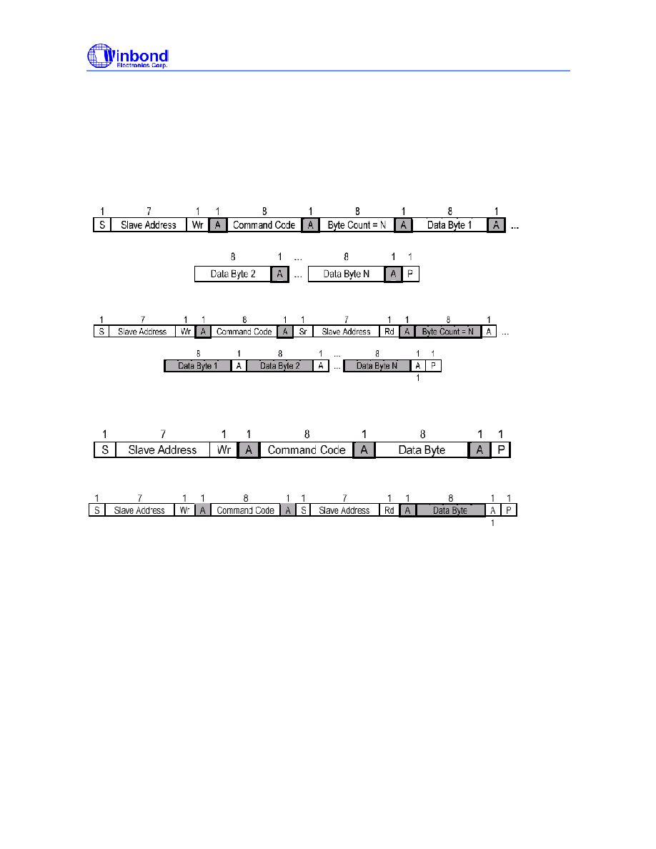
8.ACCESS INTERFACE
The W83194BR-P4X provides I
2
C Serial Bus for microprocessor to read/write internal registers. In the
W83194BR-P4X is provided Block Read/Block Write and Byte-Data Read/Write protocol. The I
2
C
address is defined at 0xD2.
Block Read and Block Write Protocol
8.1 Block Write protocol
8.2 Block Read protocol
## In block mode, the command code must filled 8'h00
8.3 Byte Write protocol
8.4 Byte Read protocol
STEPLESS CLOCK FOR VIA P4 CHIPSET
Publication Release Date: February 2003
- 16 - Revision 2.0
W83194BR-P4X
9. SPECIFICATIONS
9.1 ABSOLUTE MAXIMUM RATINGS
Stresses greater than those listed in this table may cause permanent damage to the device.
Precautions should be taken to avoid application of any voltage higher than the maximum rated
voltages to this circuit. Subjection to maximum conditions for extended periods may affect reliability.
Unused inputs must always be tied to an appropriate logic voltage level (Ground or VDD).
Parameter Rating
Absolute 3.3V Core Supply Voltage
-0.5V to +4.6V
Absolute 3.3V I/O Supple Voltage
- 0.5 V to + 4.6 V
Operating 3.3V Core Supply Voltage
3.135V to 3.465V
Operating 3.3V I/O Supple Voltage
3.135V to 3.465V
Storage Temperature
- 65
�C to + 150�C
Ambient Temperature
- 55
�C to + 125�C
Operating Temperature
0
�C to + 70�C
Input ESD protection (Human body model)
2000V
10. ORDERING INFORMATION
Part Number
Package Type
Production Flow
W83194BR-P4X
48 PIN SSOP
Commercial, 0
�C to +70�C
11. HOW TO READ THE TOP MARKING
1st line: Winbond logo and the type number: W83194BR-P4X
2nd line: Tracking code 2 8051234
2: wafers manufactured in Winbond FAB 2
8051234: wafer production series lot number
3rd line: Tracking code 814 G B B
214: packages made in '2002, week 14
G: assembly house ID; O means OSE, G means GR
A: Internal use code
B: IC revision
All the trademarks of products and companies mentioned in this data sheet belong to their
respective owners.
W83194BR-P4X
28051234
214GAB
STEPLESS CLOCK FOR VIA P4 CHIPSET
Publication Release Date: February 2003
- 17 - Revision 2.0
W83194BR-P4X
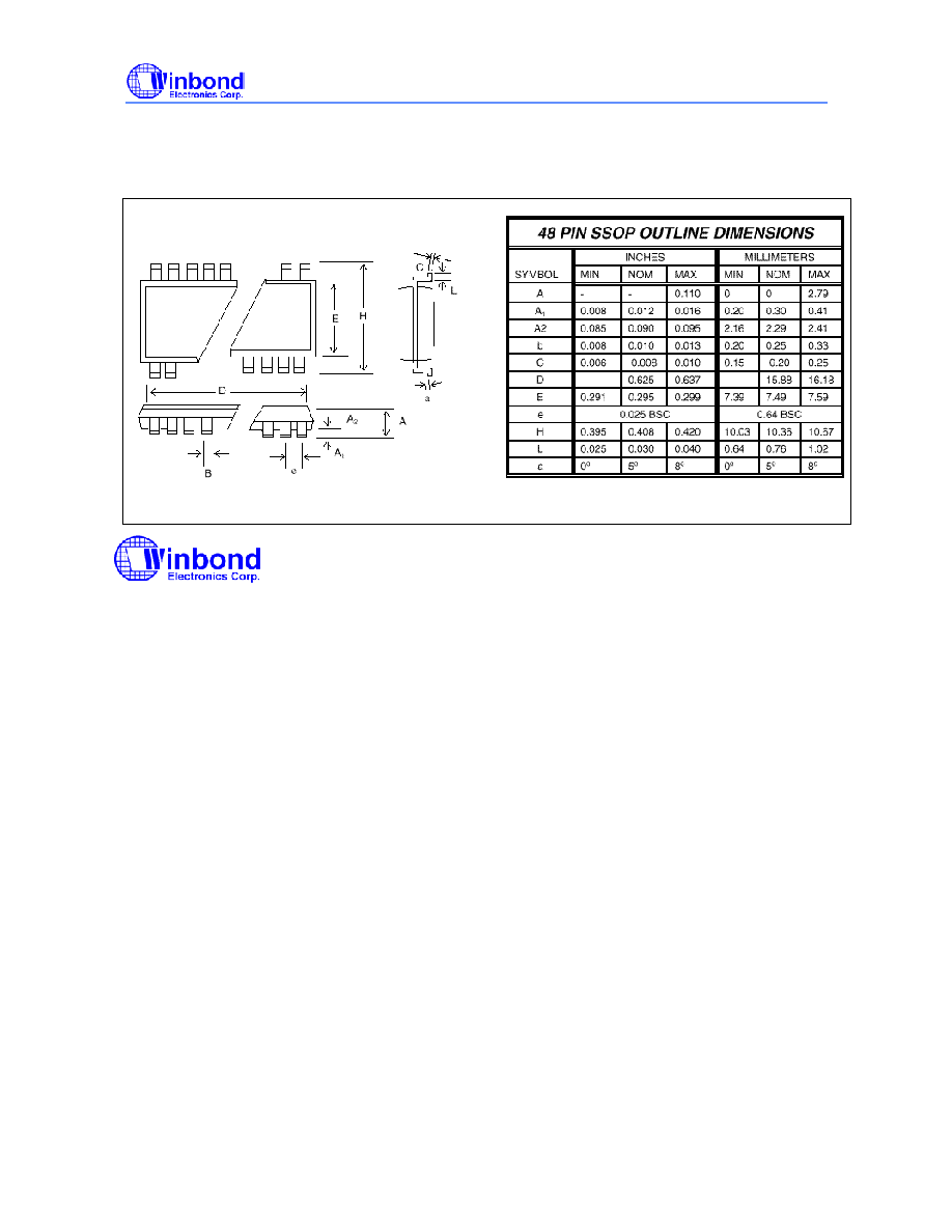
12. PACKAGE DRAWING AND DIMENSIONS
Headquarters
No. 4, Creation Rd. III
Science-Based Industrial Park
Hsinchu, Taiwan
TEL: 886-35-770066
FAX: 886-35-789467
www: http://www.winbond.com.tw/
Taipei Office
9F, No. 480, Rueiguang Road, Neihu District,
Taipei, 114, Taiwan
TEL: 886-2-81777168
FAX: 886-2-87153579
Winbond Electronics (H.K.) Ltd.
Rm. 803, World Trade Square, Tower II
123 Hoi Bun Rd., Kwun Tong
Kowloon, Hong Kong
TEL: 852-27516023-7
FAX: 852-27552064
Winbond Electronics
(North America) Corp.
2727 North First Street
San Jose, California 95134
TEL: 1-408-9436666
FAX: 1-408-9436668
Please note that all data and specifications are subject to change without notice. All the trade
marks of products and companies mentioned in this data sheet belong to their respective
owners.
These products are not designed for use in life support appliances, devices, or systems where
malfunction of these products can reasonably be expected to result in personal injury.
Winbond customers using or selling these products for use in such applications do so at their
own risk and agree to fully indemnify Winbond for any damages resulting from such improper
use or sale.