 | –≠–ª–µ–∫—Ç—Ä–æ–Ω–Ω—ã–π –∫–æ–º–ø–æ–Ω–µ–Ω—Ç: W83769 | –°–∫–∞—á–∞—Ç—å:  PDF PDF  ZIP ZIP |

W83769
LOCAL BUS IDE SOLUTION
Publication Release Date: September 1994
- 1 -
Revision A1
GENERAL DESCRIPTION
The W83769 is a high-performance, low-cost, highly integrated logic design for IDE hard disk
applications in PCI (Peripheral Component Interconnect) local bus systems. It provides a bridge
between a standard IDE drive and the PCI local bus. The W83769 is fully compatible with the ANSI
ATA 3.0 specifications for IDE hard disk operation and the PCI SIG revision 2.0 specifications for the
PCI local bus protocol. Packaged in a 100-pin PQFP, the W83769 directly supports the 32-bit PCI bus
without requiring any external TTLs.
The W83769 operates at up to 50 MHz and provides a full 32-bit data path to the PCI bus. Double-
word read and write operations are provided via internal control and conversion logic. Write posting
and read-ahead allows CPU memory cycles to run concurrently with IDE cycles and improves the
hard disk buffer-to-host transfer rate.
The IDE drive interface timing of the W83769 is completely software programmable, including
command active/recovery timing and address setup-hold timing for each drive. The device
supports Fast ATA/Enhanced IDE mode 3 timing and IORDY monitoring for better performance.
The W83769 directly supports four IDE drives with 170/1F0 dual IDE connectors. The IObase
addresses of the primary/secondary IDE connector are exchangeable by power-on strap option.
FEATURES
∑
100% PCI Local Bus 2.0 compatible
∑
IDE primary/secondary address selection
∑
32-bit local bus interface
∑
Automatic standby mode for power saving
∑
On-chip decode and select logic
∑
Supports local bus operation at up to 50 MHz
∑
Four-level pipelined read-ahead and four-level posted write buffers for concurrent system
operations
∑
Programmable parameters for command active and recovery timing
∑
Direct supports four IDE disk drives
∑
Programmable address setup timing and data active/recovery timing for each drive
∑
Slew-rate-controlled direct driving capability to interface with IDE disk
∑
Drivers for DOS, Windows, Novell, and OS/2
∑
Supports ATA 3.0 IDE standard
∑
Packaged in 100-pin PQFP
W83769
- 2 -
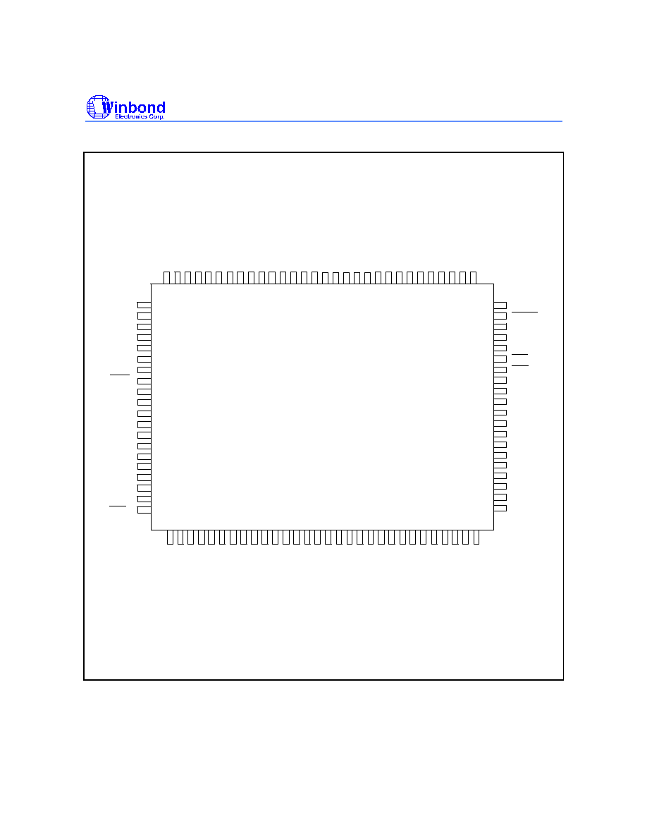
PIN CONFIGURATION
p
e
T
T
T
T
l
T
T
p
T
p
T
p
e
T
T
e
T
T
T
T
e
T
X
X
X
X
X
X
X
X
X
X
X
X
X
X
X
I
D
S
E
L
V
S
S
A
D
2
3
A
D
2
2
A
D
2
1
A
D
2
0
A
D
1
9
A
D
1
8
A
D
1
7
A
D
1
6
C
B
E
2
/
F
R
A
M
E
I
R
D
Y
T
R
D
Y
V
S
S
V
D
D
D
E
V
S
E
L
/
S
T
O
P
/
P
E
R
R
P
A
R
C
B
E
1
A
D
1
5
A
D
1
4
A
D
1
3
A
D
1
2
A
D
1
1
A
D
1
0
A
D
9
A
D
8
V
S
S
S
a
m
p
l
e
T
e
x
t
S
a
m
p
l
e
T
e
x
t
S
a
m
p
l
e
T
e
x
t
S
a
m
p
l
e
T
e
x
t
S
a
m
p
l
e
T
e
x
t
S
a
m
p
l
e
T
e
x
t
S
a
m
p
l
e
T
e
x
t
S
a
m
p
l
e
T
e
x
t
S
a
m
p
l
e
T
e
x
t
S
a
m
p
l
e
T
e
x
t
S
a
m
p
l
e
T
e
x
t
S
a
m
p
l
e
T
e
x
t
S
a
m
p
l
e
T
e
x
t
S
a
m
p
l
e
T
e
x
t
S
a
m
p
l
e
T
e
x
t
X
X
X
X
X
X
X
X
X
X
X
X
X
X
X
81
82
83
84
85
86
87
88
89
90
91
92
93
94
95
96
97
98
99
100
N.C
N.C
N.C
N.C
IRQL
V
IDEACT
RESET
CLKIN
V
AD31
AD30
AD29
AD28
AD27
AD26
AD25
AD24
CBE3
1
2 3
4
5
6 7
8
9
10 11 12 13 14 15 16 17 18 19 20 21 22 23 24 25 26 27 28 29 30
e
x
t
e
x
t
e
x
t
e
x
t
e
x
t
e
x
t
e
x
t
e
x
t
e
x
t
e
x
t
e
x
t
e
x
t
e
x
t
e
x
t
e
x
t
80 79 78 77 76 75 74 73 72 71 70 69 68 67 66 65 64 63 62 61 60 59 58 57 56 55 54 53 52 51
N
C
H
I
R
Q
/
D
R
S
T
D
S
D
7
D
S
D
6
D
S
D
5
D
S
D
4
D
S
D
3
D
S
D
2
D
S
D
1
D
S
D
0
/
D
I
O
W
/
D
I
O
R
D
S
A
2
V
S
S
V
D
D
D
S
A
1
D
S
A
0
D
S
D
8
D
S
D
9
D
S
D
1
0
D
S
D
1
1
D
S
D
1
2
D
S
D
1
3
D
S
D
1
4
D
S
D
1
5
/
D
C
S
1
/
D
C
S
0
D
R
D
Y
/
D
I
O
C
S
1
6
DD
DD
50
49
48
47
46
45
44
43
42
41
40
39
38
37
36
35
34
33
32
31
DIRQ
DSKCHG
N.C
N.C
N.C
DCS2
DCS3
N.C
V
V
AD0
AD1
AD2
AD3
AD4
AD5
AD6
AD7
CBE0
DD
SS
V
SS
V
SS
W83769
Publication Release Date: September 1994
- 3 -
Revision A1
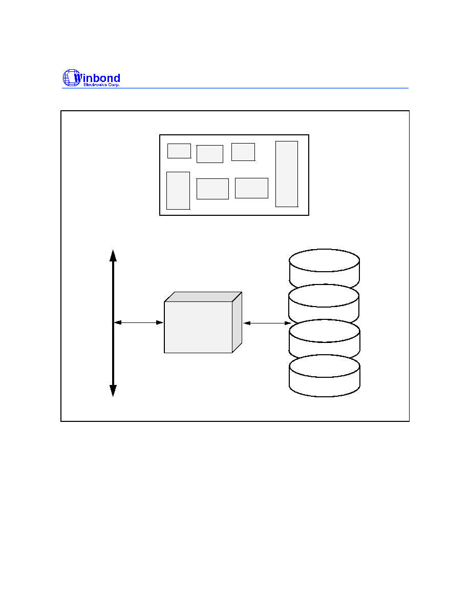
BLOCK DIAGRAM
Chip Select
Logic
Configuration
Registers
PCI
Local
Bus
Interface
4-level
Read Ahead
Buffer
4-level
Posted Write
Buffer
Read
Ahead
Counter
Direct
Drive
Interface
for
IDE
Disks
IDE Disk 1
IDE Disk 2
IDE Disk 3
IDE Disk 4
PCI Local Bus
W83769
1. FUNCTIONAL DESCRIPTION
1.1 32-bit Local Bus Interface
The W83769 is a Local Bus IDE Interface device that serves as an interface between standard IDE
hard disks and a high-performance local bus. It is fully compatible with the PCI Local Bus 2.0
standard.
The W83769 provides all the required pins and logic needed for direct connection to the CPU bus,
including the 32-bit data bus. The chip can be mounted on a local bus adapter card using the PCI
Local Bus standard or mounted directly onto the motherboard.

W83769
- 4 -
1.2 Chip Decode and Select Logic
The W83769 contains all required chip select and decode logic needed to function without any
additional buffering or interface logic to the local bus. This includes all address decoding, data
buffering, and control logic.
1.3 Direct Drive IDE Disk Interface
The W83769 provides a slew-rate-controlled direct drive interface to four IDE drives. The interface
conforms to relevant industry standards, including the ANSI ATA Rev. 3.0 standard. Up to four
W83769 devices, and therefore 16 IDE drives, can be interfaced to the local bus. Additional drives
can reside on expansion buses. Drive selection and switching are handled by software.
Each device permits either of the two interfaced IDE ports to be assigned and addressed as the
primary or secondary port. Each port can support two drives, which can be assigned as the master
drive (drive 0) or slave drive (drive 1). Individual IDE disk drive performance can be optimized
through the W83769's programmable registers. Each drive's command active and recovery timing,
address setup and hold, and data read/write active and recovery timing may be controlled
independently.
1.4 Four-level Read Ahead Buffer and Counter
The W83769's read-ahead feature significantly enhances disk drive read performance. In pipelined
read-ahead mode, when the host CPU is occupied with other or previous data transfers, the IDE
controller can automatically request and concurrently transfer additional data from the disk drive.
These data are stored in the device's four-level FIFO read-ahead buffer.The controller will continue to
read data from the drive as long as the buffer is not full, the read-ahead counter is not zero, and the
host CPU continues to request data. Data transfer sizes are determined by the host CPU request and
can be word or double-word.
A programmable read-ahead counter is used in conjunction with the read-ahead buffer to regulate the
flow of data from the disk drive. The counter is normally initialized with the number of bytes per
sector. This is determined from the disk formatting and can be different for each drive. As data is
transferred, the counter is decremented to zero. It is then reinitialized for the next sector transfer.
1.5 Four-level Posted Write Buffer
The W83769 also contains a four-level FIFO posted-write buffer which can be used by the CPU to
pipeline data to the disk drive, thereby significantly increasing throughput. The CPU data are written
to the posted-write buffer. Concurrently, data are written to the disk drive by the IDE controller at the
appropriate data transfer rate. While the buffered data are waiting to be written, the CPU is left free to
fetch additional data for the next transfer.
1.6 Interrupt Operation
To ensure proper interrupt operation between the IDE drives and the host CPU, the drives' interrupts
can be passed through the W83769. The interrupts are input on the DIRQ pin and asynchronously
output to the host chipset on the HIRQ pin as IRQ14, the standard IDE PC/AT interrupt. If four drives,
i.e., two drive cables, are present, the interrupts from both pairs of drives can be connected to HIRQ.
The interrupt status of individual drives can be read from the general purpose configuration register,
RX50, bit 2. A 10K ohm pullup should be connected to the HIRQ input to prevent floating.
Alternatively, with four drives present, the interrupt from each pair of drives can be connected directly
to the host CPU chipset IRQ14 and IRQ15.

W83769
Publication Release Date: September 1994
- 5 -
Revision A1
1.7 3F7h Register Operation
The disk drive status register 3F7h is a read-only register that provides hard drive status in bits 6-0 to
the host CPU. Floppy drive status is provided as bit 7; this status indication originates from pin 34 of
the floppy drive cable. All 8 bits can be combined, buffered, and passed to the host CPU chipset as a
normal ISA bus cycle. The W83769 will detect the 3F7h address on the host address bus as an IDE
cycle but will not generate any clocked transfer cycle.
1.8 Power-Save Mode
The W83769 contains a power-save feature for notebook or green PC applications. If no IDE cycles
are in progress, the power-save circuitry forces all but the CPU tracking and address decoding logic
into a static state to reduce power consumption. This also reduces EMI radiation because the IDE
cable is inactive while the device is in power-save mode.
1.9 Reset Initialization
The first step in setting up the W83769 for operation is to reset the device using the active high
RESET pin. A reset immediately terminates any operation in progress and returns the W83769 to a
known state from which it can be initialized. Immediately following a reset, the controller determines
its operational mode via pin configuration.
If the IDEACT pin is sampled high, IDE operation will be enabled, and disk transfer cycles can be
executed. If the IDEACT pin is sampled low, IDE operation is disabled, and the controller will respond
only to configuration cycles via the general purpose I/O ports. This permits BIOS software to test the
system for installed disks and enable/disable the W83769 and specific features and operations.
1.10 Hardware Configurations
Several hardware configuration options can be defined using the DSA1 and DCS0
1
-
pins during the
power-on reset:
DSA1
Digital Input Register
0
Disable
1
Enable
DCS0
1
-
Device ID selection
(for multiple chip only)
00
60h
01
61h
10
62h
11
63h
To select the value of 0 for each bit in the above configuration, the corresponding pin needs to be
pulled down during the power-on reset. Pulling the pin up will set the value to 1.
1.11 I/O Registers

W83769
- 6 -
A number of I/O registers are implemented in W83769 that allow the chip to be programmed by
system software. These I/O registers can be divided into two categories: PCI configuration registers
and general purpose registers. This section defines the possible settings of these registers.
Underlined register settings designate the default values of the registers at power-on.
1.11.1 PCI Configuration Registers
In the PCI mode, the PCI configuration read/write will set up the PCI configuration registers.
Host Address 0
-
1(VID)
Vendor ID (RO)
10ADh for Winbond
Host Address 2
-
3(DID)
Device ID (RO)
0001h for W83769
Host Address 4
-
5 (PCMD)
PCI Command Register (R/W)
bit 15
-
9:
reserved
bit 8
-
7:
always 0
bit 6:
parity checking
0
disable
1
enable
bit 5
-
1:
always 0
bit 0:
always 1
Host Address 6
-
7 (PSTTS)
Device Status Register (R/W)
bit 15:
parity error detected
bit 14
-
11:
always 0
bit 10
-
9:
DEVSEL timing (RO)
00
fast
01
medium
10
slow
11
reserved
bit 8
-
0:
reseved
Host Address 8 (REVID)

W83769
Publication Release Date: September 1994
- 7 -
Revision A1
Revision ID (RO)
00h for Rev BB
02h for Rev A3C
Host Address 9 (PGIF)
Programming Interface (RO)
00h
Host Address Ah (SUBCLS)
Sub-Class (RO)
01h for IDE Controller
Host Address Bh (BASCLS)
Base Class (RO)
01h for Mass Storage
Controller
Host Address 3Ch (INTLINE)
Interrupt Line (RO)
0Eh (value of 14)
Host Address 3Dh (INTPIN)
Interrupt Pin (RO)
01h (value of 1)

W83769
Publication Release Date: September 1994
- 8 -
Revision A1
1.11.2 General Purpose Registers
Two IO ports are used to access the entire set of general purpose I/O registers: the index port at
address 0B4h and the data port at 0B8h. To access a register, first write the index into the index port
and then read or write the data throgh the data port. The index and data port can be relocated to
address 034h and 038h by pulling up the DSA2 pin. Every internal register is assigned an 8-bit index.
The general purpose registers allow driver software to program the IDE controller to work with
different hard disks with various characteristics. The majority of the registers defined here are related
to the hard disk's timing parameters.
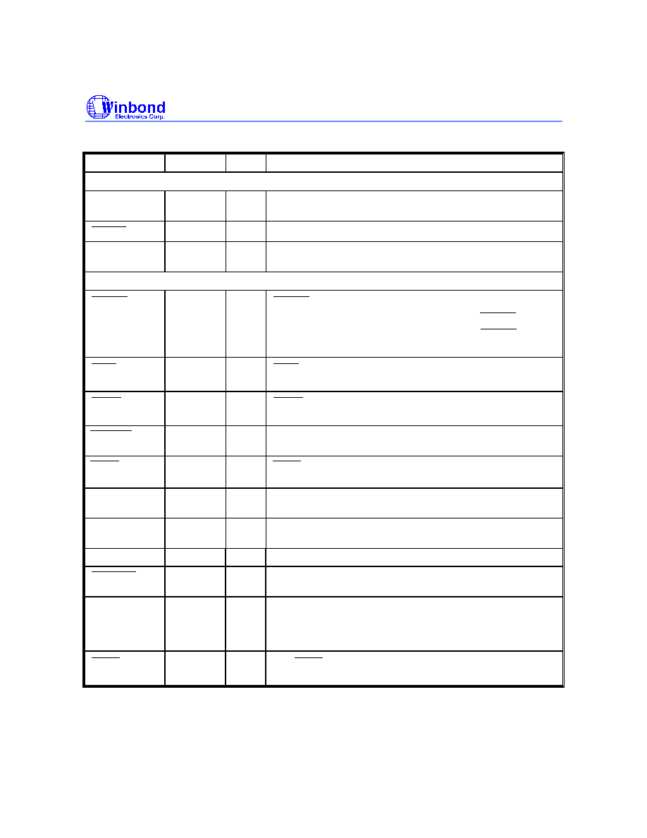
RX50 (CFR)
Device Configuration Register (RO)
bit 7:
reserved
bit 6:
Digital Input register
0
disable
1
enable
bit 5:
reserved
bit 4,3:
Device ID selection
00
60h
01
61h
10
62h
11
63h
bit 2
IDE drive interrupt status
(read CFR will clear this bit)
0
no interrupt pending
1
interrupt pending
bit 1:
reserved
bit 0:
enable/disable 2nd IDE port (R/W)
0
disable
1
enable
Note that RX50 is read-only, with the exception of bit 0. This bit is for enabling or disabling the second
IDE port and therefore is a read/write bit. This bit is writable through RX50 but is readable only
through RX57.
RX51 (CNTRL)
Control Register (R/W)
bit 7:
reserved
bit 6:
Read ahead enable
0
enable
1
disable

W83769
Publication Release Date: September 1994
- 9 -
Revision A1
bit 5:
Host write fifo/reg longer data hold time
0
enable
1
disable
bit 4:
PCI parity check
0
disable
1
enable
bit 3:
timing selection for drives of secondary port
0
disks 0,2 use timing set 0 and disks 1,3 use timing set 1
1
disks 0,1 use timing set 0 and disks 2,3 use timing set 1
bit 2:
DEVESL timing
0
medium
1
fast
bit 1:
Host write timing
0
slow timing
1
fast timing
bit 0:
Host read timing
0
slow timing
1
fast timing
RX52 (CMDTLM)
IDE Command Timing Register (RW)
bit 7
-
4:
IOR\W active count
0000
16 clocks
0001
2 clocks
0010
2 clocks
0011
3 clocks
0100
4 clocks
0101
5 clocks
0110
6 clocks
0111
7 clocks
1000
8 clocks
1001
9 clocks
1010
10 clocks
1011
11 clocks
1100
12 clocks
1101
13 clocks

W83769
- 10 -
1110
14 clocks
1111
15 clocks
bit 3
-
0:
Command Recovery count
0000
16 clocks
0001
1 clocks
0010
2 clocks
0011
3 clocks
0100
4 clocks
0101
5 clocks
0110
6 clocks
0111
7 clocks
1000
8 clocks
1001
9 clocks
1010
10 clocks
1011
11 clocks
1100
12 clocks
1101
13 clocks
1110
14 clocks
1111
15 clocks
RX53 (ARTIM0)
Drive 0 Address Setup/Data Recovery Timing Register (R/W)
bit 7
-
6:
address set up count
00
3 clocks
01
1 clocks
10
2 clocks
11
4 clocks
bit 5
-
4:
reserved
bit 3
-
0:
Data (1F0h) recovery count
0000
16 clocks (read/write)
0001
4 clocks (read)
5 clock (write)
0010
4 clocks (read)
5 clock (write)
0011
5 clocks (read/write)
0100
6 clocks (read/write)
0101
7 clocks (read/write)
0110
8 clocks (read/write)

W83769
Publication Release Date: September 1994
- 11 -
Revision A1
0111
9 clocks (read/write)
1000
10 clocks (read/write)
1001
11 clocks (read/write)
1010
12 clocks (read/write)
1011
13 clocks (read/write)
1100
14 clocks (read/write)
1101
15 clocks (read/write)
1110
16 clocks (read/write)
1111
17 clocks (read/write)
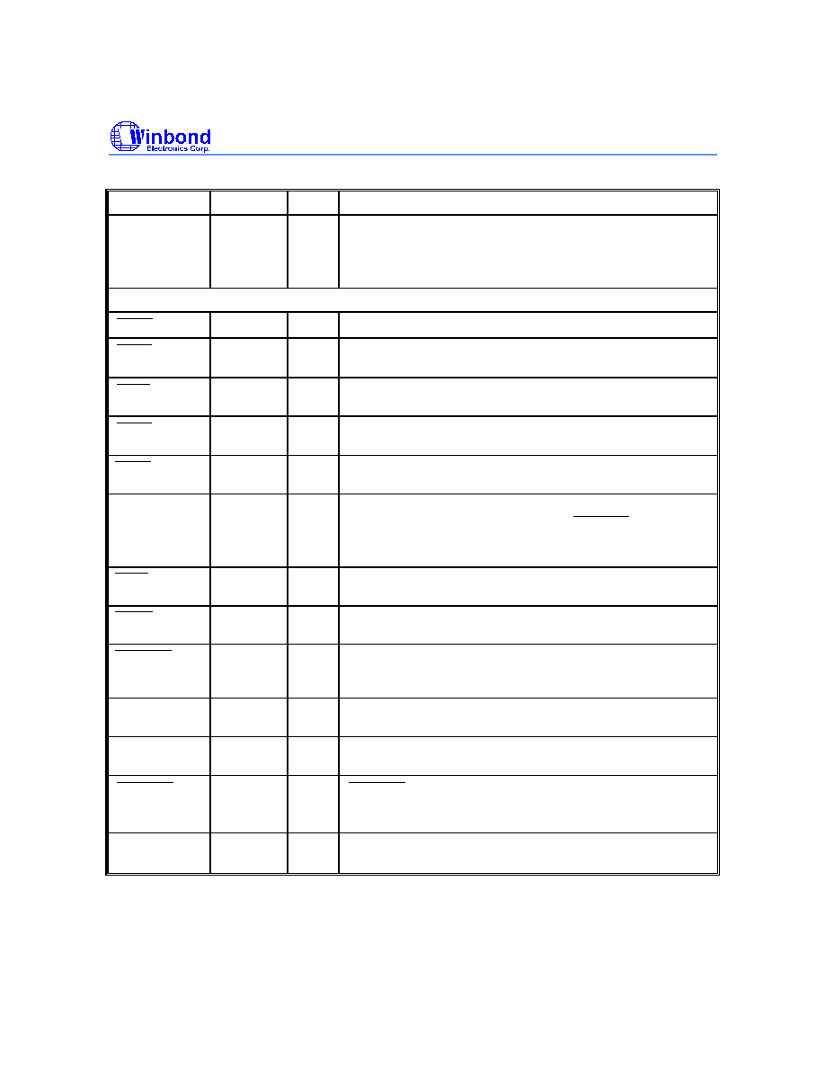
RX54 (DRWTLM0)
Drive 0 Data Read/Write Active Timing Register (R/W)
bit 7
-
4:
Data read active count
0000
16 clocks
0001
2 clocks
0010
2 clocks
0011
3 clocks
0100
4 clocks
0101
5 clocks
0110
6 clocks
0111
7 clocks
1000
8 clocks
1001
9 clocks
1010
10 clocks
1011
11 clocks
1100
12 clocks
1101
13 clocks
1110
14 clocks
1111
15 clocks
bit 3
-
0:
Data write active count
0000
16 clocks
0001
2 clocks
0010
2 clocks
0011
3 clocks

W83769
- 12 -
0100
4 clocks
0101
5 clocks
0110
6 clocks
0111
7 clocks
1000
8 clocks
1001
9 clocks
1010
10 clocks
1011
11 clocks
1100
12 clocks
1101
13 clocks
1110
14 clocks
1111
15 clocks
RX55 (ARTIM1)
Drive 1 Address Setup/Data Recovery Timing Register (R/W)
bit 7
-
6:
address set up count
00
3 clocks
01
1 clocks
10
2 clocks
11
4 clocks
bit 5
-
4:
reserved
bit 3
-
0:
Data (1F0h) recovery count
0000
16 clocks (read/write)
0001
4 clocks (read)
5 clocks (write)
0010
4 clocks (read)
5 clock (write)
0011
5 clocks (read/write)
0100
6 clocks (read/write)
0101
7 clocks (read/write)
0110
8 clocks (read/write)
0111
9 clocks (read/write)
1000
10 clocks (read/write)
1001
11 clocks (read/write)
1010
12 clocks (read/write)
1011
13 clocks (read/write)

W83769
Publication Release Date: September 1994
- 13 -
Revision A1
1100
14 clocks (read/write)
1101
15 clocks (read/write)
1110
16 clocks (read/write)
1111
17 clocks (read/write)
RX56 (DRWTIM1)
Drive 1 Data Read/Write Active Timing Register (R/W)
bit 7
-
4:
Data read active count
0000
16 clocks
0001
2 clocks
0010
2 clocks
0011
3 clocks
0100
4 clocks
0101
5 clocks
0110
6 clocks
0111
7 clocks
1000
8 clocks
1001
9 clocks
1010
10 clocks
1011
11 clocks
1100
12 clocks
1101
13 clocks
1110
14 clocks
1111
15 clocks
bit 3
-
0:
Data write active count
0000
16 clocks
0001
2 clocks
0010
2 clocks
0011
3 clocks
0100
4 clocks
0101
5 clocks
0110
6 clocks
0111
7 clocks
1000
8 clocks
1001
9 clocks

W83769
- 14 -
1010
10 clocks
1011
11 clocks
1100
12 clocks
1101
13 clocks
1110
14 clocks
1111
15 clocks
RX57 (GR1)
General Register #1 (R/W)
bit 7
-
1:
reserved
bit 0:
enable/disable 2nd IDE port
0
disable
1
enable
Bit 0 of RX57 is related to bit 0 of RX50. Refer to the description of RX50 above.
RX58 (GR2)
General Register #2 (R/W)
bit 7
-
0:
reserved
RX59 (BRSTLNG)
Burst Length Control Register (R/W)
bit 7
-
0:
Burst length (in double words)
40h (default value is 256 bytes)
W83769
Publication Release Date: September 1994
- 15 -
Revision A1
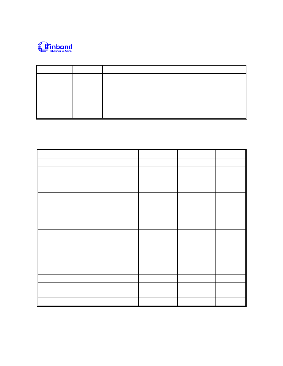
2. SIGNAL DESCRIPTION
NAME
NO.
TYPE
DESCRIPTION
CLOCK AND RESET
CLKIN
89
I
Input clock to the W83769. This clock has the same
frequency as the local bus clock.
RESET
88
I
Reset pin from local bus to reset the chip.
IDEACT
87
I
Chip enable pin. When set high, the W83769 is enabled
after reset. When set low, the W83769 is disabled.
HOST INTERFACE
FRAME
12
I
FRAME is driven by the current master to indicate the
beginning and duration of an access. While FRAME is
asserted, data transaction continues. When FRAME is de-
asserted, the transaction is in the final data phase.
IRDY
13
I
IRDY indicates the PCI bus master can complete the
current data phase of the transaction.
TRDY
14
B
TRDY indicates the PCI bus slave can complete the current
data phase of the transaction.
DEVSEL
17
O
The W83769 drives this signal active to indicate that it has
decoded its address as the target of the current access.
STOP
18
B
STOP indicates the W83769 is requesting that the current
master stop the current transaction.
IDSEL
1
I
IDSEL is asserted by PCI system to select the W83769
during configuration read and write transactions.
PAR
20
B
The W83769 drives PAR in read data phases for parity
checking.
HIRQ
79
O
IRQ14 output to the system chip set.
CBE0
3
-
31, 21,
11, 100
I
These inputs are the multiplexed Bus Command and Byte
Enable signals on the PCI bus.
IRQL
85
I
The IRQL pin controls the polarity of the HIRQ output. When
this pin is tied high, the polarity of HIRQ will follow that of
DIRQ (pin 50). When this pin is tied low, the polarity of
HIRQ will be the reverse of that of DIRQ.
PERR
19
B
The PERR pin reports data parity errors during data read
phases.
W83769
- 16 -
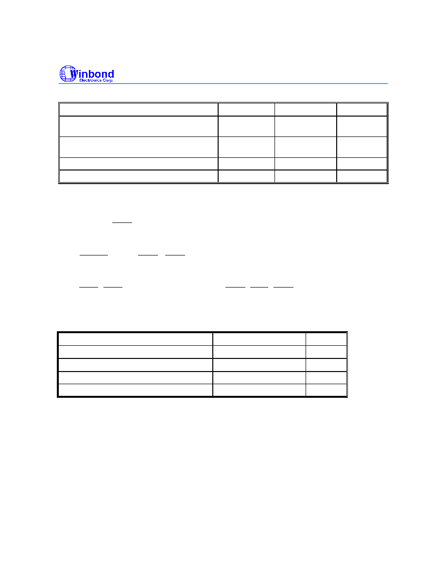
Signal Description, continued
NAME
NO.
TYPE
DESCRIPTION
AD31
-
0
92
-
99,
3
-
10
22
-
29,
32
-
39
B
These bidirectional signals are the multiplexed Address and
Data on the PCI bus.
DIRECT IDE DRIVE INTERFACE
DRST
78
O
Reset signal to the IDE drives.
DCS0
53
B
Chip select signal for IDE drive 0, 1 task file registers 1F0H
-
1F7H. During power-on reset, this pin is an input.
DCS1
54
B
Chip select signal for IDE drive 0, 1 task file registers 3F6H
and 3F7H. During power-on reset, this pin is an input.
DCS2
45
O
Chip select signal for IDE drive 2, 3 task file registers 170H
-
177H.
DCS3
44
O
Chip select signal for IDE drive 2, 3 task file registers 376H
and 377H.
DSA0
-
2
63, 64, 67
B
These signals are the IDE disk drive address bits 0-2.
DSA0
-
2 are to be used together with
DCS0
3
-
to decode
the individual IDE task file registers. During power-on reset,
these pins are inputs.
DIOR
68
O
Disk IO read command signal to initiate a read access from
IDE drives.
DIOW
69
O
Disk IO write command signal to initiate a write access to
IDE drives.
DIOCS16
51
I
IO cycle 16-bit select input from the IDE drives. When this
pin is driven low, it indicates the IDE drives are ready to
send/receive a 16-bit word.
DRDY
52
I
Disk drive ready signal. Indicates that the IDE drives have
completed the current command cycle.
DIRQ
50
I
Interrupt request from the IDE drives to generate the HIRQ
output.
DSKCHG
49
I
DSKCHG
is connected to pin 34 of a floppy disk connector.
This active low input pin indicates the status of port 3F7, bit
7, which is reported from the floppy disk controller.
DSD15
-
0
55
-
62,
77
-
70
B
16-bit disk data bus.
W83769
Publication Release Date: September 1994
- 17 -
Revision A1
Signal Description, continued
NAME
NO.
TYPE
DESCRIPTION
N.C.
V
SS
V
DD
43, 46
-
48,
80
-
84
2, 15, 30,
40, 42, 66,
90
16, 41, 65,
86, 91
DC TEST SPECIFICATIONS
Power supply definition: V
DD
= +5.0 Volts +/- 5%, V
SS
= system ground
SYMBOL IDENTIFICATION
MINIMUM
MAXIMUM
UNIT
I
DD
Power supply current (static)
---
20.0
mA
I
DD
Power supply current (dynamic)
---
50.0
mA
L
IL
Low Input leakage current
(inputs other than pull-up inputs)
(@ V
IN
= V
SS
)
---
+/- 10
µ
A
L
IL
Low Input leakage current
(inputs with pull-up structure)
(@ V
IN
= V
SS
)
-300.0
10
µ
A
L
IH
High Input leakage current
(inputs with pull-down structure
(@ V
IN
= V
DD
)
-300.0
10
µ
A
L
IH
High Input leakage current
(inputs other than pull-down inputs)
(@ V
IN
= V
DD
)
---
+/- 10
µ
A
Z
IL
Low IO Tri-State leakage current
(@ V
IN
= V
SS
)
---
+/- 10
µ
A
Z
IH
High IO Tri-State leakage current
(@ V
IN
= V
DD
)
---
+/- 10
µ
A
V
IL
(TTL) Logic Low Input Level
---
0.8
V
V
IH
(TTL) Logic High Input Level
2.0
---
V
V
IL
(CMOS) Logic Low Input Level
---
0.8
V
V
IH
(COMS) Logic High Input Level
3.5
---
V
W83769
- 18 -
DC Test Specifications, continued
SYMBOL IDENTIFICATION
MINIMUM
MAXIMUM
UNIT
V
OL
Output Logic Low Level
* output sink of 8.0, 12.0, 18.0 mA
0.45
V
V
OH
Output Logic High Level
* Output source of -8.0, -12.0, -18.0 mA
2.4
V
C
IN
Capacitance Input
---
10.0
pF
C
OUT
Capacitance Output
---
10.0
pF
PCLK V
IL
MIN = 2.1 Volts
8 mA output drive current pins:
AD[31:0],
PERR
, PAR
12 mA output drive current pins:
DEVSEL
, HIRQ,
TRDY
,
STOP
18 mA output drive current pins:
DCS0
-
DCS3 , DSA0
-
DSA2, DSD15
-
DSD0, DRST, DIOR, DIOW
ABSOLUTE MAXIMUM RATINGS
PARAMETER
RATING
UNIT
Case Temperature Under Bias
-65 to 110
∞
C
Storage Temperature
-65 to 150
∞
C
Supply Voltage with Respect to Ground
-0.5 to V
DD
+ 0.5
V
Voltage on Any Pin
-0.5 to V
DD
+ 0.5
V
Note: Exposure to conditions beyond those listed under Absolute Maximum Ratings may adversely affect the life and reliability of the
device.

W83769
Publication Release Date: September 1994
- 19 -
Revision A1
(See APP.doc, 3 pages)

W83769
- 20 -

W83769
Publication Release Date: September 1994
- 21 -
Revision A1
Headquarters
No. 4, Creation Rd. III,
Science-Based Industrial Park,
Hsinchu, Taiwan
TEL: 886-3-5770066
FAX: 886-3-5792646
http://www.winbond.com.tw/
Voice & Fax-on-demand: 886-2-7197006
Taipei Office
11F, No. 115, Sec. 3, Min-Sheng East Rd.,
Taipei, Taiwan
TEL: 886-2-7190505
FAX: 886-2-7197502
Winbond Electronics (H.K.) Ltd.
Rm. 803, World Trade Square, Tower II,
123 Hoi Bun Rd., Kwun Tong,
Kowloon, Hong Kong
TEL: 852-27516023
FAX: 852-27552064
Winbond Electronics North America Corp.
Winbond Memory Lab.
Winbond Microelectronics Corp.
Winbond Systems Lab.
2730 Orchard Parkway, San Jose,
CA 95134, U.S.A.
TEL: 1-408-9436666
FAX: 1-408-9436668
Note: All data and specifications are subject to change without notice.