W83791SD/W83791SG
Publication Release Date: January 18, 2005
- III -
Revision 1.1
Table of Contents-
1.
GENERAL DESCRIPTION ......................................................................................................... 1
2.
FEATURES ................................................................................................................................. 1
3.
KEY SPECIFICATIONS .............................................................................................................. 2
4.
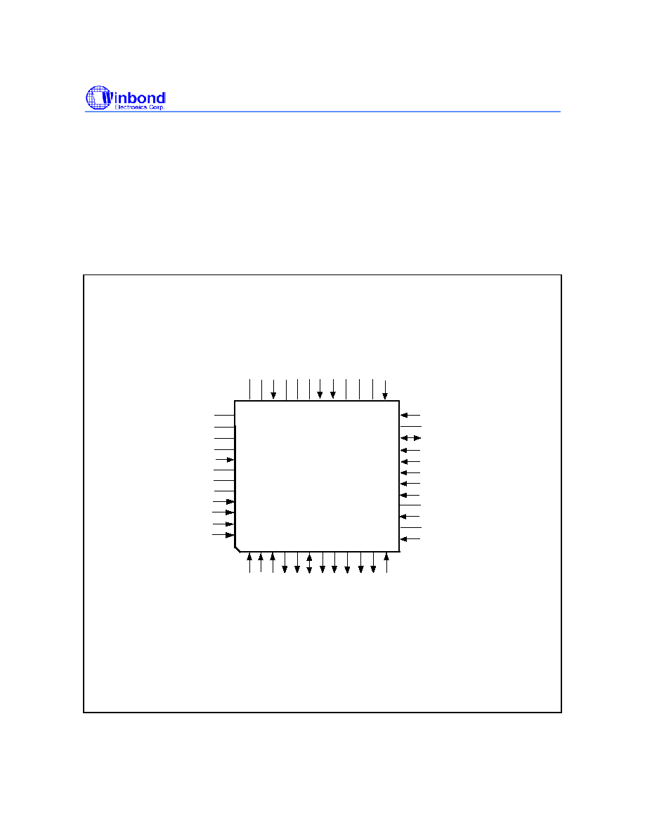
PIN CONFIGURATION ............................................................................................................... 2
5.
PIN DESCRIPTION..................................................................................................................... 3
6.
FUNCTION DESCRIPTION ........................................................................................................ 4
6.1
Speech Function............................................................................................................. 4
6.1.1
General Description..........................................................................................................4
6.1.2
Event Trigger Queue ........................................................................................................4
6.1.3
Connection of EEPROM...................................................................................................5
6.1.4
Speaker Output ................................................................................................................6
7.
CONTROL AND STATUS REGISTER ....................................................................................... 6
7.1
Speech Flash Memory Address Registers
Index 00h-02h (Bank 0).......................... 6
7.2
Speech Flash Memory Data Registers
Index 03h-06h (Bank 0) ............................... 6
7.3
Event Trigger Timeout Register
Index 08h (Bank 0).................................................. 7
7.4
Speech Programmable Trigger Register
Index 09h (Bank 0).................................... 8
7.5
Speech Input Trigger Property Register
Index 0Ah (Bank 0) .................................... 8
7.6
Speech Flash Memory Read Data Registers
Index 0Dh-0Eh (Bank 0)..................... 8
7.7
User Defined Registers
Index 18h-1Ch (Bank 0)....................................................... 9
7.8
Speech Control Register 1
Index 1Fh (Bank 0) ......................................................... 9
7.9
Serial Bus Address Register
Index 48h (Bank 0)....................................................... 9
7.10
Device ID
Index 49h (Bank 0) .................................................................................... 9
7.11
Disable Abnormal BEEP Control Register
Index 4Dh (Bank 0)............................... 10
7.12
High Byte Access
Index 4Eh (Bank 0) ..................................................................... 10
7.13
Winbond Vendor ID
Index 4Fh (Bank 0) .................................................................. 10
7.14
Winbond Test Register
Index 50h - 55h (Bank 0).................................................... 10
7.15
Chip ID -- Index 58h (Bank 0) ....................................................................................... 10
7.16
Speech Flash Memory Read Data Registers
Index A4h-A5h (Bank 0)................... 11
7.17
Flash Page count
Index A7h (Bank 0) ..................................................................... 11
8.
ELECTRICAL CHARACTERISTICS......................................................................................... 11
8.1
Absolute Maximum Ratings .......................................................................................... 11
8.2
DC Characteristics........................................................................................................ 11
8.3
AC Characteristics ........................................................................................................ 13
8.3.1
Serial Bus Timing Diagram.............................................................................................13
9.
HOW TO READ THE TOP MARKING...................................................................................... 14
10.
PACKAGE SPECIFICATION .................................................................................................... 15
11.
APPLICATION CIRCUITS ........................................................................................................ 16

W83791SD/W83791SG
Publication Release Date: January 18, 2005
- 1 -
Revision 1.1
1. GENERAL DESCRIPTION
W83791SD/SG is a programmable speech synthesizer with 9-bit current DAC output that can connect
to speaker or LINE_OUT by the AC'97 audio codec. It supports 1 CPU present or absent event trap, 5
external event traps, and 127 internal programmable event traps to trigger maximum 133 different
speech output. If more than two events happen simultaneously, the priority set is: SLOTOCC# >
EVNTRP1 > EVNTRP2 > EVNTRP3 > EVNTRP4 > EVNTRP5 > 127 Programmable events (Bank0
index 09h).
For the application of error messages from BIOS, 127 Programmable events are enabled with a watch
dog timer. The time interval is programmable and events will be triggered when time out.
External flash memory interface with Winbond W55FXX is flexible to change warning voice message
and support on-line programming flash data through I
2
C
TM
interface. An external resistor is added to
provide ring oscillator.
Through the application software or BIOS, the users can edit and change the voice database in the
serial flash chip by themselves under O.S. A free Windows AP --- Voice Editor
TM
is provided for the
voice editing, which can accept the *.wav file as the voice database resource. Users can replace the
voice with which they like through the S/W.
W83791SD/SG also provides two addresses setting pins A0 & A1 for different I
2
C
TM
address and can
be connected up to 4 devices if necessary.
2. FEATURES
Speech Item
� Programmable speech synthesizer
� New high fidelity synthesis algorithm
� Build in 8-bit current D/A converter
� Instruction
cycle 400
�S typically
� Section control provided in each voice section
Variable frequency: 4.8/6/8/12 KHz
� External resistor for ring oscillator
� 1 CPU present or absent trigger input
� 5 External trigger inputs
� 127 Internal programmable trigger inputs with a watch dog timer
� Programmable 0-255 seconds timeout trigger inputs
General
� I
2
C
TM
serial bus interface
� 2 pins (A0, A1) to provide selectable address setting for application of multiple devices (up to 4
devices) wired through I
2
C
TM
interface
� Winbond hardware monitoring application software (Voice Editor
TM
) support, for both Windows
95/98/ME/2000 and Windows NT 4.0/5.0
� Internal clock Oscillator with 3M Hz
� 5V
V
DD
operation