
W83877TF
WINBOND I/O

WINBOND I/O
W83877TF
Publication Release Date: March 1998
- 1 -
Preliminary Version 0.61
GENERAL DESCRIPTION
The W83877TF is an enhanced version from Winbond's most popular I/O chip W83877F --- which
integrates the disk drive adapter, serial port (UART), IrDA 1.0 SIR, parallel port, configurable Plug-
and-Play registers for the whole chip --- plus additional powerful features:
ACPI / legacy power
management,
serial IRQ, and IRQ sharing.
The disk drive adapter functions of W83877TF include a floppy disk controller compatible with the
industry standard 82077/765, data separator, write pre-compensation circuit, decode logic, data rate
selection, clock generator, drive interface control logic, interrupt and DMA logic. The wide range of
functions integrated into the W83877TF greatly reduces the number of components required for
interfacing with floppy disk drives. The W83877TF supports four 360K, 720K, 1.2M, 1.44M, or 2.88M
disk drives and data transfer rates of 250 Kb/S, 300 Kb/S, 500 Kb/S,1 Mb/S, and 2 Mb/S.
The W83877TF provides two high-speed serial communication ports (UARTs), one of which supports
serial Infrared communication. Each UART includes a 16-byte send/receive FIFO, a programmable
baud rate generator, complete modem control capability, and a processor interrupt system. One of
the UARTs support infrared (IR) IrDA1.0. Both UARTs provide legacy speed with baud rate up to
115.2K and provide advanced speed with baud rate up to
230k, 460k, and 921k bps which support
higher speed Modems.
The W83877TF supports one PC-compatible printer port (SPP), Bi-directional printer port (BPP) and
also Enhanced Parallel Port (EPP) and Extended Capabilities Port (ECP). Through the printer port
interface pins, also available are: Extension FDD Mode and Extension 2FDD Mode allowing one or
two external floppy disk drives to be connected.
This function is especially valuable for notebook
computer applications.
Winbond W83877TF provides functions that comply with
ACPI (Advanced Configuration and Power
Interface), which includes support of legacy and ACPI power management through SMI or SCI
function pins. One 24-bits power management timer is implemented with the carry notify interrupt.
W83877TF also has auto power management mode to reduce the power consumption.
The
serial IRQ for PCI architecture is supported, ISA IRQs (IRQ1~IRQ15) can be cascaded into one
IRQSER pin. W83877TF also features ISA bus
IRQ sharing and allows two or more devices to share
the same IRQ pin.
W83877TF is made to fully comply with
Microsoft
TM
PC97 Hardware Design Guide. IRQs, DMAs,
and I/O space resources are flexible to adjust to meet ISA PnP requirement. Moreover W83877TF is
made to meet the specification of PC97's requirement in the power management:
ACPI and DPM
(Device Power Management).
The configuration registers support mode selection, function enable/disable, and power down function
selection. Furthermore, the configurable PnP registers are compatible with the Plug-and-Play feature
demand of Windows 95
TM
, which makes system resource allocation more efficient than ever.
Another benefit of W83877TF is that it is pin-to-pin compatible to W83877F, and all of the 100-pin
Winbond I/O IC family. Thus makes the design of applications very convenient and flexible.

W83877TF
Publication Release Date: March 1998
- 40 -
Version 0.61
3.2 Register Address
TABLE 3-1 UART Register Bit Map
Bit Number
Register Address Base
0
1
2
3
4
5
6
7
8
BDLAB = 0
Receiver
Buffer
Register
(Read Only)
RBR
RX Data
Bit 0
RX Data
Bit 1
RX Data
Bit 2
RX Data
Bit 3
RX Data
Bit 4
RX Data
Bit 5
RX Data
Bit 6
RX Data
Bit 7
8
BDLAB = 0
Transmitter
Buffer Register
(Write Only)
TBR
TX Data
Bit 0
TX Data
Bit 1
TX Data
Bit 2
TX Data
Bit 3
TX Data
Bit 4
TX Data
Bit 5
TX Data
Bit 6
TX Data
Bit 7
9
BDLAB = 0
Interrupt Control
Register
ICR
RBR Data
Ready
Interrupt
Enable
(ERDRI)
TBR
Empty
Interrupt
Enable
(ETBREI)
USR
Interrupt
Enable
(EUSRI)
HSR
Interrupt
Enable
(EHSRI)
0
0
0
0
A
Interrupt Status
Register
(Read Only)
ISR
"0" if
Interrupt
Pending
Interrupt
Status
Bit (0)
Interrupt
Status
Bit (1)
Interrupt
Status
Bit (2)**
0
0
FIFOs
Enabled
**
FIFOs
Enabled
**
A
UART FIFO
Control
Register
(Write Only)
UFR
FIFO
Enable
RCVR
FIFO
Reset
XMIT
FIFO
Reset
DMA
Mode
Select
Reserved
Reversed
RX
Interrupt
Active Level
(LSB)
RX
Interrupt
Active Level
(MSB)
B
UART Control
Register
UCR
Data
Length
Select
Bit 0
(DLS0)
Data
Length
Select
Bit 1
(DLS1)
Multiple
Stop Bits
Enable
(MSBE)
Parity
Bit
Enable
(PBE)
Even
Parity
Enable
(EPE)
Parity
Bit Fixed
Enable
PBFE)
Set
Silence
Enable
(SSE)
Baud rate
Divisor
Latch
Access Bit
(BDLAB)
C
Handshake
Control
Register
HCR
Data
Terminal
Ready
(DTR)
Request
to
Send
(RTS)
Loopback
RI
Input
IRQ
Enable
Internal
Loopback
Enable
0
0
0
D
UART Status
Register
USR
RBR Data
Ready
(RDR)
Overrun
Error
(OER)
Parity Bit
Error
(PBER)
No Stop
Bit
Error
(NSER)
Silent
Byte
Detected
(SBD)
TBR
Empty
(TBRE)
TSR
Empty
(TSRE)
RX FIFO
Error
Indication
(RFEI) **
E
Handshake
Status Register
HSR
CTS
Toggling
(TCTS)
DSR
Toggling
(TDSR)
RI Falling
Edge
(FERI)
DCD
Toggling
(TDCD)
Clear
to Send
(CTS)
Data Set
Ready
(DSR)
Ring
Indicator
(RI)
Data Carrier
Detect
(DCD)
F
User Defined
Register
UDR
Bit 0
Bit 1
Bit 2
Bit 3
Bit 4
Bit 5
Bit 6
Bit 7
8
BDLAB = 1
Baudrate Divisor
Latch Low
BLL
Bit 0
Bit 1
Bit 2
Bit 3
Bit 4
Bit 5
Bit 6
Bit 7
9
BDLAB = 1
Baudrate
Divisor Latch
High
BHL
Bit 8
Bit 9
Bit 10
Bit 11
Bit 12
Bit 13
Bit 14
Bit 15
*: Bit 0 is the least significant bit. The least significant bit is the first bit serially transmitted or received.
**: These bits are always 0 in 16450 mode.
W83877TF
Publication Release Date: March 1998
- 41 -
Version 0.61
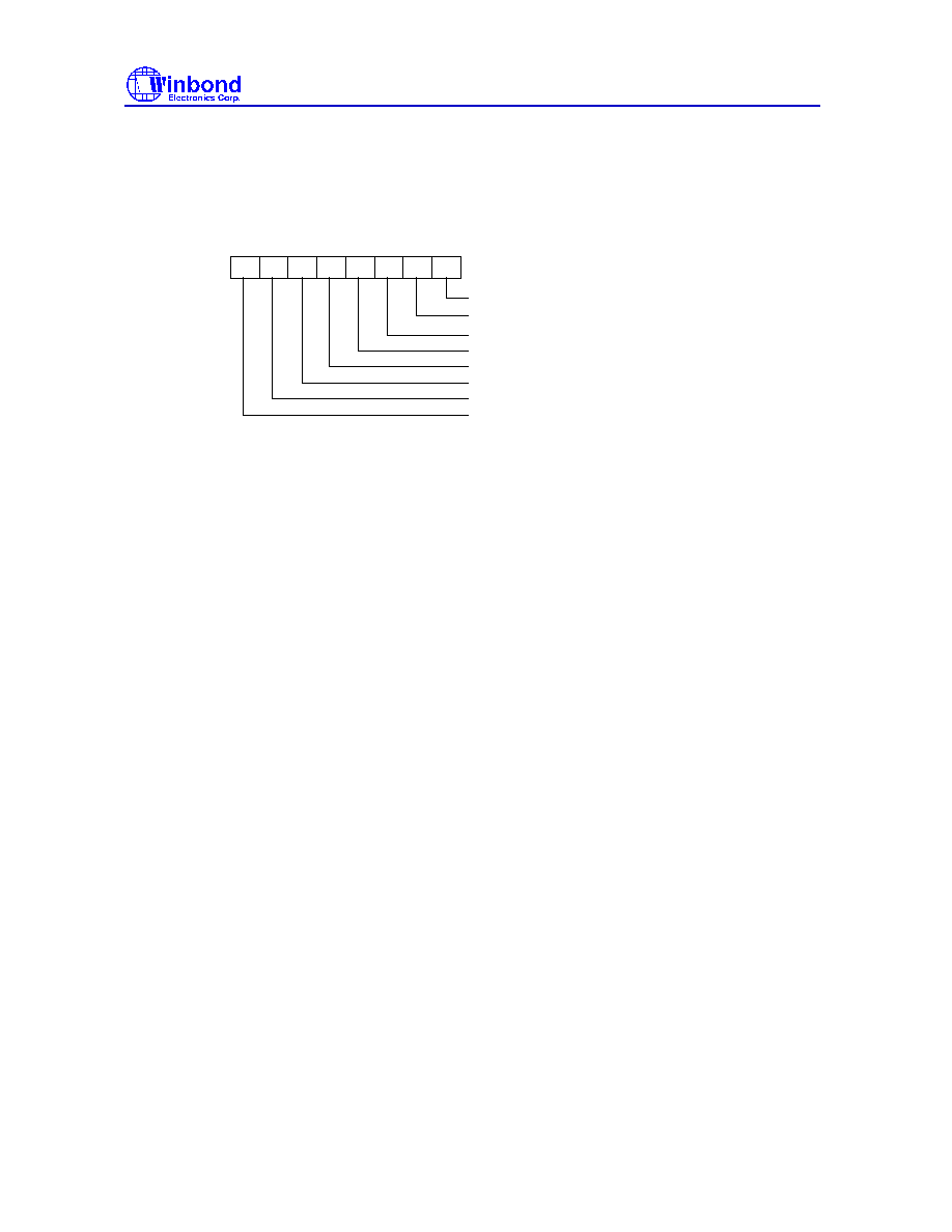
3.2.1 UART Control Register (UCR) (Read/Write)
The UART
Control Register controls and defines the protocol for asynchronous data communications,
including data length, stop bit, parity, and baud rate selection.
1
2
3
4
5
6
7
0
Data length select bit 0 (DLS0)
Data length select bit 1(DLS1)
Multiple stop bits enable (MSBE)
Parity bit enable (PBE)
Even parity enable (EPE)
Parity bit fixed enable (PBFE)
Set silence enable (SSE)
Baudrate divisor latch access bit (BDLAB)
Bit 7: BDLAB. When this bit is set to a logical 1, designers can access the divisor (in 16-bit binary
format) from the divisor latches of the baud rate generator during a read or write operation.
When this bit is reset, the Receiver Buffer Register, the Transmitter Buffer Register, or the
Interrupt Control Register can be accessed.
Bit 6: SSE. A logical 1 forces the Serial Output (SOUT) to a silent state (a logical 0). Only SOUT is
affected by this bit; the transmitter is not affected.
Bit 5: PBFE. When PBE and PBFE of UCR are both set to a logical 1,
(1) if EPE is a logical 1, the parity bit is fixed as a logical 0 to transmit and check.
(2) if EPE is a logical 0, the parity bit is fixed as a logical 1 to transmit and check.
Bit 4: EPE. This bit describes the number of logic 1's in the data word bits and parity bit only when bit
3 is programmed. When this bit is set, an even number of logic 1's are sent or checked. When
the bit is reset, an odd number of logic 1's are sent or checked.
Bit 3: PBE. When this bit is set, the position between the last data bit and the stop bit of the SOUT
will be stuffed with the parity bit at the transmitter. For the receiver, the parity bit in the same
position as the transmitter will be detected.
Bit 2: MSBE. This bit defines the number of stop bits in each serial character that is transmitted or
received.
(1) If MSBE is set to a logical 0, one stop bit is sent and checked.
(2) If MSBE is set to a logical 1, and data length is 5 bits, one and a half stop bits are sent and
checked.
(3) If MSBE is set to a logical 1, and data length is 6, 7, or 8 bits, two stop bits are sent and
checked.
Bits 0 and 1: DLS0, DLS1. These two bits define the number of data bits that are sent or checked in
each serial character.

W83877TF
Publication Release Date: March 1998
- 42 -
Version 0.61
TABLE 3-2 WORD LENGTH DEFINITION
DLS1
DLS0
DATA LENGTH
0
0
5 bits
0
1
6 bits
1
0
7 bits
1
1
8 bits
3.2.2 UART Status Register (USR) (Read/Write)
This 8-bit register provides information about the status of the data transfer during communication.
1
2
3
4
5
6
7
0
RBR Data ready (RDR)
Overrun error (OER)
Parity bit error (PBER)
No stop bit error (NSER)
Silent byte detected (SBD)
Transmitter Buffer Register empty (TBRE)
Transmitter Shift Register empty (TSRE)
RX FIFO Error Indication (RFEI)
Bit 7: RFEI. In 16450 mode, this bit is always set to a logic 0. In 16550 mode, this bit is set to a logic
1 when there is at least one parity bit error, no stop bit error or silent byte detected in the FIFO.
In 16550 mode, this bit is cleared by reading from the USR if there are no remaining errors left
in the FIFO.
Bit 6: TSRE. In 16450 mode, when TBR and TSR are both empty, this bit will be set to a logical 1. In
16550 mode, if the transmit FIFO and TSR are both empty, it will be set to a logical 1. Other
than these two cases, this bit will be reset to a logical 0.
Bit 5: TBRE. In 16450 mode, when a data character is transferred from TBR to TSR, this bit will be
set to a logical 1. If ETREI of ICR is a logical 1, an interrupt will be generated to notify the CPU
to write the next data. In 16550 mode, this bit will be set to a logical 1 when the transmit FIFO
is empty. It will be reset to a logical 0 when the CPU writes data into TBR or FIFO.
Bit 4: SBD. This bit is set to a logical 1 to indicate that received data are kept in silent state for a full
word time, including start bit, data bits, parity bit, and stop bits. In 16550 mode, it indicates the
same condition for the data on top of the FIFO. When the CPU reads USR, it will clear this bit
to a logical 0.