W83C42
KEYBOARD CONTROLLER
Publication Release Date: July 1994
- 1 - Revision A3
GENERAL DESCRIPTION
The W83C42 keyboard controller is programmed to support the IBM
Æ
compatible personal computer
keyboard serial interface. The keyboard controller receives serial data from the keyboard, checks the
parity of the data, translates the scan code, and presents the data to the system as a byte of data in
its output buffer. The controller will interrupt the system when data is placed in its output buffer. The
byte of data will be sent to the keyboard serially with an odd parity bit automatically inserted. The
keyboard is required to acknowledge all data transmissions. No transmission should be sent to the
keyboard until acknowledge is received for the previous byte sent.
Winbond Electronics Corporation has developed a fast keyboard controller and BIOS to improve the
performance of IBM PC/AT
Æ
386
TM
DX/SX and 486
TM
DX/SX machines and their compatibles. Hardwire
methodology is used in this keyboard controller instead of software implementation, as in the
traditional 8042 keyboard BIOS. This enables the keyboard controller to respond instantly to all
commands sent from the keyboard to the CPU BIOS.
The keyboard controller enables popular programs such as AutoCAD
Æ
, Microsoft
Æ
Windows
TM
3.1,
NOVELL
Æ
, and other programs to run much faster.
FEATURES
∑
Supports IBM PC/AT 386DX/SX and 486 DX/SX system designs
∑
Runs much faster than traditional keyboard controllers
∑
Host interface compatible with traditional keyboard controller
∑
6MHz~12MHz operating frequency
∑
Communicates with keyboard directly
∑
High-reliability CMOS technology
∑
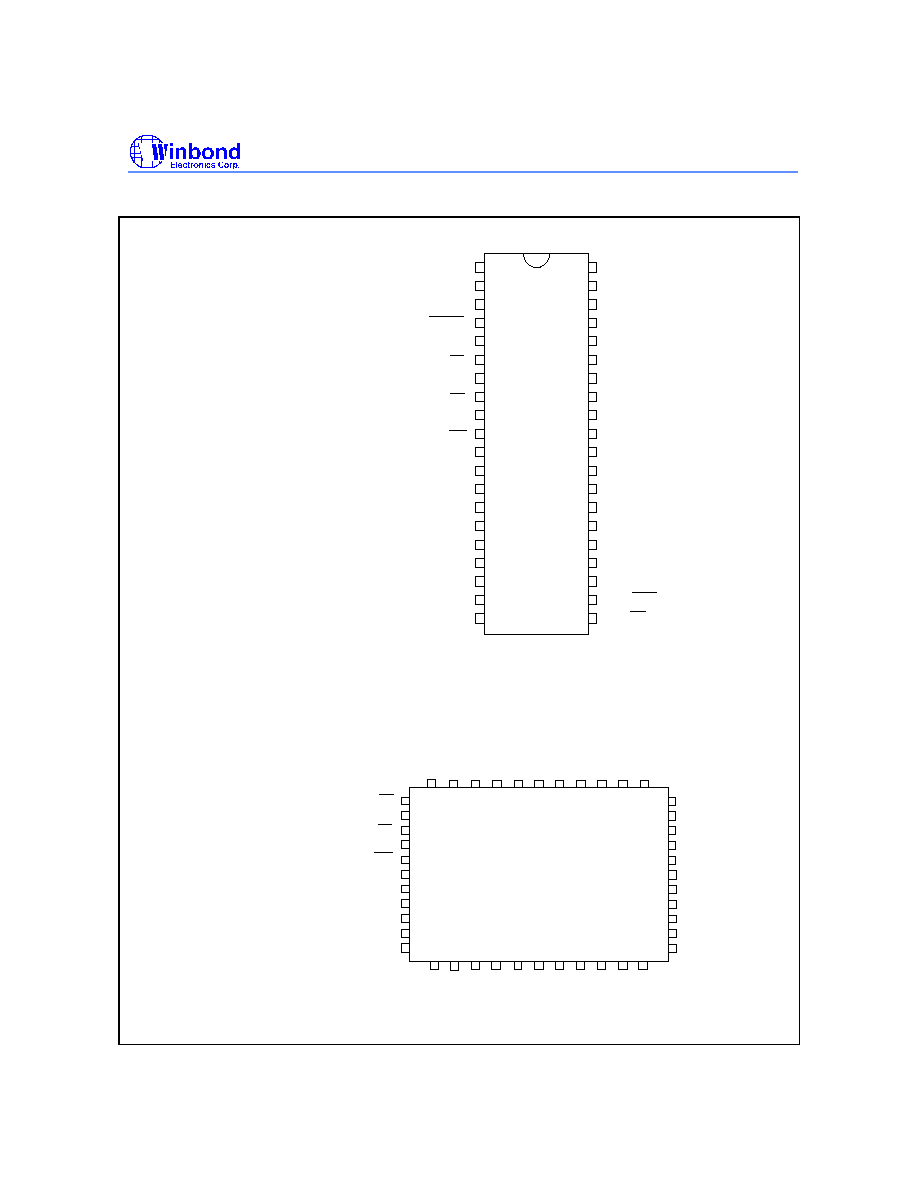
Available packages: 40-pin DIP, 44-pin PLCC
IBM and PC/AT are registered trademarks of International Business Machines Corporation. 386 and 486 are trademarks of Intel
Corporation. AutoCAD is a registered trademark of Autodesk, Inc. Microsoft is a registered trademark and Windows is a trademark of
Microsoft Corporation. NOVELL is a registered trademark of Novell, Inc.
W83C42
Publication Release Date: July 1994
- 3 - Revision A3
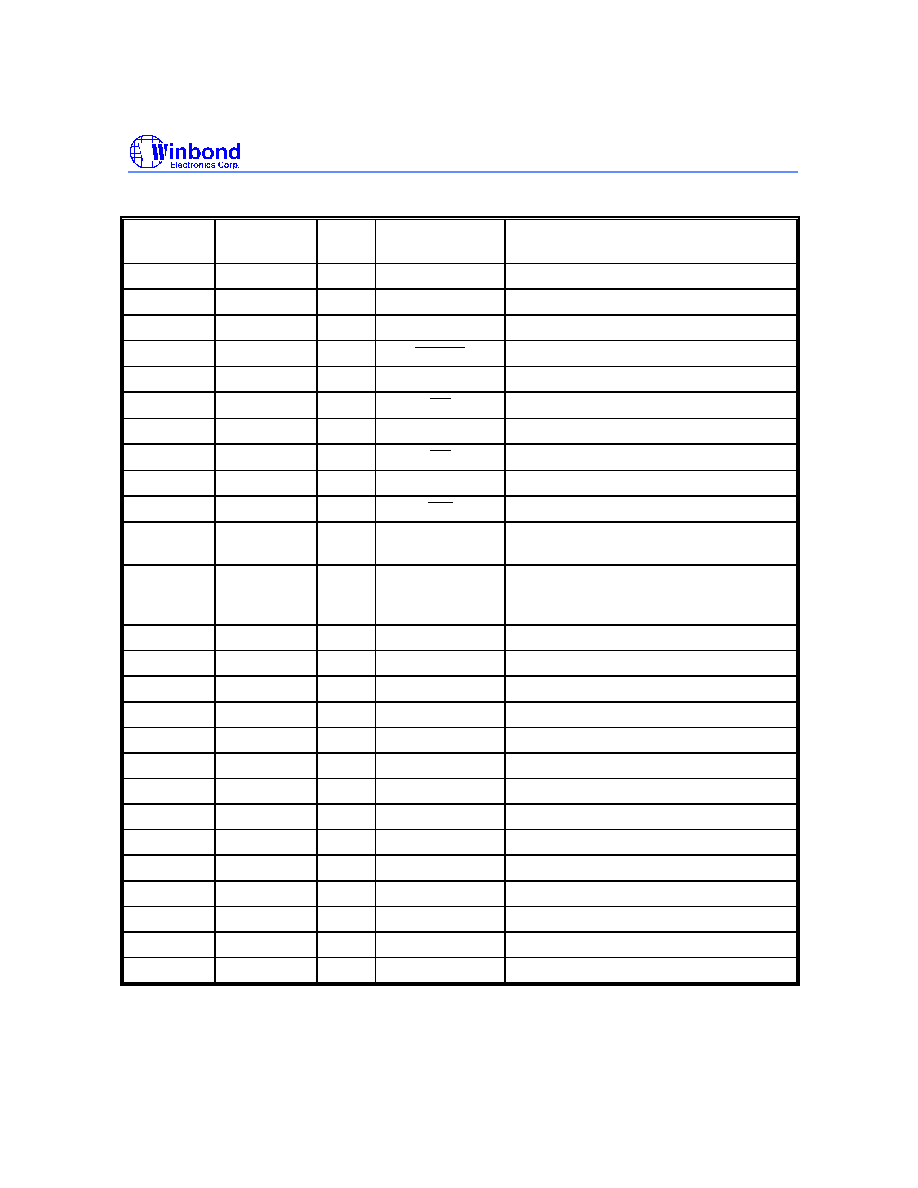
PIN DESCRIPTION
PIN NO.
(
40-pin DIP)
PIN NO.
(
44-pin PLCC)
I/O
NAME
FUNCTION
1
2
I
T0
K/B Clock Input
2
3
I
X
IN
Crystal Clock I/P
3
4
O
X
OUT
Crystal Clock O/P
4
5
I
RESET
Chip Reset
5
6
-
V
DD
Optional +5V Power Supply
6
7
I
CS
Chip Select
7
8
-
V
SS
Optional Ground Power
8
9
I
RD
I/O Read
9
10
I
A2
Connect to Address A2
10
11
I
WR
I/O Write
11, 26
1, 12, 13,
23, 29, 34
-
NC
Reserved
12, 13, 14,
15, 16, 17,
18, 19
14, 15, 16,
17, 18, 19,
20, 21
I/O
D0-D7
Data Bus D0 - D7
20
22
-
V
SS
Ground Power Supply
21
24
O
P20
Bit 0 of Port 2 (RCB: System Reset)
22
25
O
P21
Bit 1 of Port 2 (GA20: GATE A20)
23
26
I/O
P22
Bit 2 of Port 2
24
27
I/O
P23
Bit 3 of Port 2
25
28
-
V
DD
Optional +5V Power Supply
27
30
I/O
P10
Bit 0 of Port 1
28
31
I/O
P11
Bit 1 of Port 1
29
32
I/O
P12
Bit 2 of Port 1
30
33
I/O
P13
Bit 3 of Port 1
31
35
I
P14
Bit 4 of Port 1 (RAM Jumper Select)
32
36
I
P15
Bit 5 of Port 1 (JUMP)
33
37
I
P16
Bit 6 of Port 1 (Display Select)
34
38
I
P17
Bit 7 of Port 1 (K/B Inhibit Switch)
W83C42
- 4 -
Pin Description, continued
PIN NO.
(
40-pin DIP)
PIN NO.
(
44-pin PLCC)
I/O
NAME
FUNCTION
35
39
O
P24
Bit 4 of Port 2 (OBF O/P Interrupt)
36
40
O
P25
Bit 5 of Port 2 (I/P Buffer Empty)
37
41
O
P26
Bit 6 of Port 2 (K/B Clock O/P)
38
42
O
P27
Bit 7 of Port 2 (K/B Data O/P)
39
43
I
T1
K/B Data Input
40
44
-
V
DD
+5V Power Supply
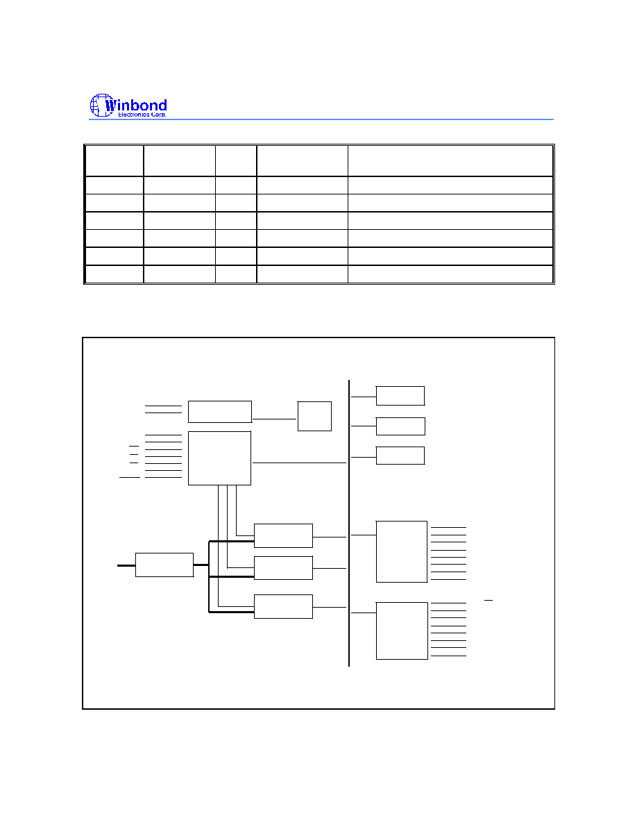
BLOCK DIAGRAM
RECEIVE
HARDWIRE
SELECT
DATA
BUFFER
REGISTER
REGISTER
STATUS
PORT
INTERFACE
STATUS
INPUT
T0
T1
XOUT
XIN
WR
RD
CS
A2
D0 - D7
R64
SCAN
CODE
ROM
CONTROL
LOGIC
RESET
P1 0
P1 1
P1 2
P1 3
P1 4 (RAM Select)
P1 5 (Manufacture Mode)
P1 6 (Display)
P1 7 (KBNH)
P2 0 (RC)
P2 1 (Gate A20)
P2 2
P2 3
P2 4
P2 5
P2 6 (Keyboard Clock)
P2 7
CONTROL &
BUFFER
REGISTER
BUFFER
REGISTER
OUTPUT
BUFFER
REGISTER
W60
W64
R60
INPUT &
OUTPUT
PORT
INTERFACE
OUTPUT
(Keyboard Data)
CONTROL
TRANSMIT
TRANSMIT
REGISTER
W83C42
Publication Release Date: July 1994
- 5 - Revision A3
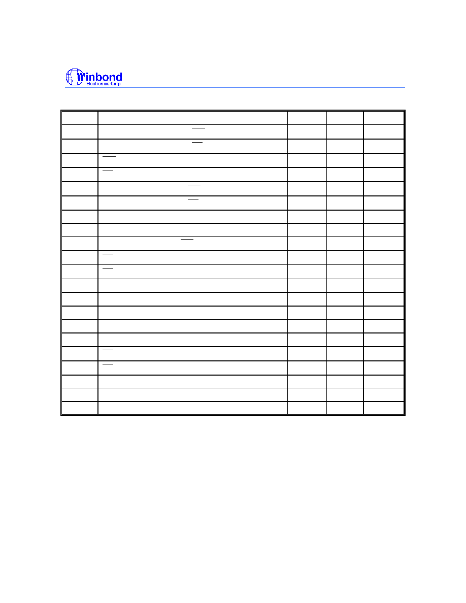
AC TIMING
NO.
DESCRIPTION
MIN.
MAX.
UNIT
T1
Address Setup Time from WR
0
nS
T2
Address Setup Time from RD
0
nS
T3
WR Strobe Width
20
nS
T4
RD Strobe Width
20
nS
T5
Address Hold Time from WR
0
nS
T6
Address Hold Time from RD
0
nS
T7
Data Setup Time
50
nS
T8
Data Hold Time
0
nS
T9
Gate Delay Time from WR
10
nS
T10
RD to Drive Data Delay
20
nS
T11
RD to Floating Data Delay
0
20
nS
T12
Data Valid After Clock Falling (SEND)
4
µ
S
T13
K/B Clock Period
20
µ
S
T14
K/B Clock Pulse Width
10
µ
S
T15
Data Valid Before Clock Falling (RECEIVE)
4
µ
S
T16
K/B ACK After Finish Receiving
20
µ
S
T17
RC Fast Reset Pulse Delay (8 MHz)
2
3
µ
S
T18
RC Pulse Width (8 MHz)
6
µ
S
T19
Transmit Timeout
2
mS
T20
Data Valid Hold Time
0
µ
S
T21
X
IN
/X
OUT
Period ( 6-12 MHz )
83
167
nS