
DATA BOOK
W83C553F
SYSTEM I/O
CONTROLLER
WITH PCI
ARBITER
A
Company
Publication number: 2565; Version A.7.0d.1


Copyright Notice
Copyright 1995, 1996, 1997
WINBOND SYSTEMS
LABORATORY.
All rights reserved.
Issued: September 27, 1995
Publication no: 2565; Ver. A.6
Issued: October 1, 1996
Publication no: 2565; Ver. A.6.2
Issued: March 1, 1997
Publication no: 2565; Ver. A.7.0b
Issued: September 1, 1997
Publication no: 2565; Ver.A.7.0c
Issued: February 22, 1998
Publication no. 2565; Ver.A.7.0d
Disclaimer
This document contains information
on a product under development at
WINBOND SYSTEMS
LABORATORY. The information is
intended to help you to evaluate this
product. WINBOND SYSTEMS
LABORATORY reserves the right to
change or discontinue work on this
proposed product without notice.
WINBOND SYSTEMS
LABORATORY makes no warranty
for the use of its products and bears
no responsibility for any errors which
appear in this document.
Specifications are subject to change
without notice.
Trademarks
The company and product names mentioned in
this document may be the trademarks or
registered trademarks of their manufacturers.
W I N B O N D
SYSTEMS
LABORATORY
2727 North First Street,
San Jose, CA 95134
USA

W83C553F Table of Contents
WINBOND SYSTEMS LABORATORY
1
PREFACE
This document describes the function and use of the Winbond Systems Laboratory W83C553F System I/O (SIO) Controller
with PCI arbiter. It provides all of the information necessary for design engineers to incorporate the device into notebook
and desktop computer systems.
Organization of the Manual
The information in this document is organized into the following seven chapters:
Chapter 1
General information
This consists of an overview discussion of the product and
its features. Included are the stylistic conventions used in
this manual.
Chapter 2
Pin Descriptions
Provides pin-out diagrams and pin descriptions.
Chapter 3
System Architecture
Discusses the design of the device and the implementation
of the device's features.
Chapter 4
Register Information
Describes the software control of the chip set's various
functions.
Chapter 5
Electrical Specifications
Provides the operating specifications for the device.
Chapter 6
Timing Diagrams
Provides timing diagrams and tables of timing values.
Chapter 7
Mechanical Description
Shows the critical dimensions of the device.
Chapter 8
Thermal Information
Shows the temperature calculation of the device.
Appendix A
I/O Driver Characteristics

W83C553F Table of Contents
WINBOND SYSTEMS LABORATORY
2

W83C553F Table of Contents
WINBOND SYSTEMS LABORATORY
3
TABLE OF CONTENTS
Preface............................................................................................................................................... 1
1.0 General Information ................................................................................................... 5
1.1 Features .................................................................................................................... 5
1.2 General Description ................................................................................................... 7
1.3 Stylistic Conventions Used in this Manual .................................................................. 9
2.0 Pin Descriptions ................................................................................................................... 10
2.1 Pin Assignments ........................................................................................................ 10
2.2 Pin Description........................................................................................................... 13
3.0 System Architecture............................................................................................................. 28
3.1 Overview ................................................................................................................... 28
3.2 Active State ............................................................................................................... 29
3.3 Bus Structures ........................................................................................................... 30
3.4 PCI-to-ISA Bridge ...................................................................................................... 31
3.5 PCI Bus Cycles.......................................................................................................... 31
3.6 PCI I/O Read Cycle ................................................................................................... 34
3.7 PCI I/O Write Cycle ................................................................................................... 35
3.8 PCI Configuration Read Cycle ................................................................................... 36
3.9 PCI Configuration Write Cycle ................................................................................... 37
3.10 PCI Memory Read ..................................................................................................... 38
3.11 PCI Memory Write ..................................................................................................... 39
3.12 PCI Memory Read Line.............................................................................................. 40
3.13 PCI Memory Write and Invalidate .............................................................................. 40
3.14 Transaction Termination ............................................................................................ 41
3.14.1 PCI Disconnect With Data Transfer Timing ................................................ 41
3.14.2 PCI Disconnect Without Data Transfer Timing ........................................... 42
3.14.3 PCI Target Abort Timing ............................................................................ 43
3.14.4 PCI Preemption Timing .............................................................................. 44
3.14.5 PCI Master Abort Timing ............................................................................ 45
3.15 IDE Interface Operation ............................................................................................. 46
3.16 PIO Transfers ............................................................................................................ 47
3.17 32-Bit Data Transfers ................................................................................................. 48
3.18 Bus Master Transfers................................................................................................. 49
3.19 82C59A Interrupt Controller ....................................................................................... 49
3.20 82C37A DMA Controller............................................................................................. 49
3.21 82C54 Counter/Timer ................................................................................................ 50
3.22 PCI Arbiter ................................................................................................................. 50
3.23 Break Events ............................................................................................................. 51
3.24 CPU Modes (X86 or PowerPC) .................................................................................. 51
4.0 Register Information ............................................................................................................ 52
4.1 PCI Configuration Space - ISA Bridge Registers (Function 0) .................................... 54
4.1.1 Function 0 Header Registers ...................................................................... 54
4.1.2 Function 0 Control Registers ...................................................................... 58
4.2 ISA Bridge (Function 0) I/O Registers ........................................................................ 78
4.2.1 DMA Controller I/O Registers ..................................................................... 78
4.2.2 Programmable Interrupt Controller (PIC) Registers .................................... 93
4.2.3 Counter/Timer I/O Registers....................................................................... 101
4.2.4 Miscellaneous I/O Control Registers........................................................... 105
4.3 PCI Configuration Space - Bus Master IDE Registers (Function 1)............................ 109
4.3.1 Function 1 Header Registers ............................................................................. 111

W83C553F Table of Contents
WINBOND SYSTEMS LABORATORY
4
4.3.2 Function 1 Control Registers ...................................................................... 123
4.4 Bus Master IDE (Function 1) I/O Registers................................................................. 1
29
4.4.1 Primary/Secondary Command Registers .................................................... 13
0
4.4.2 Primary/Secondary Status Registers .......................................................... 13
1
4.4.3 Primary/Secondary PRD
Table
.................................................................. 13
2
5.0 Electrical Specifications ...................................................................................................... 13
3
6.0 Timing Diagrams .................................................................................................................. 13
5
6.1 PCI Timing Diagrams................................................................................................. 13
6
6.2 IDE/ATA Data Transfers ............................................................................................ 14
2
6.3 ISA Bus Timing.......................................................................................................... 15
0
7.0 Mechanical Description ....................................................................................................... 15
3
8.0 Thermal Information ..............................................................................................154
9.0 Appendix A............................................................................................................155

W83C553F General Information
WINBOND SYSTEMS LABORATORY
5
1.0 GENERAL INFORMATION
1.1 Features
High Integration PCI-ISA solution
� Optimized for lowest system cost
� Complies with PCI Revision 2.0 specification
� Universal PCI device supporting x86 and PowerPC (non-x86) modes of operation
Nand tree on most signal pins to facilitate board level testing in PCB manufacturing environment
Integrated PCI Bus Master IDE controller
� Dual channel Bus Master IDE for up to 4 peripherals, including hard drives, ATAPI (IDE) CD-ROMs,
tapes, etc.
� Multi-threading capability allows two simultaneous I/O processes
� Independent IDE Timing registers allow fast/slow devices on the same cable
� Two independent DMA channels for Bus Master scatter/gather DMA transfers across the PCI bus
� Large 64 byte DMA FIFO for zero wait state PCI burst transfers
� Support for multiword DMA Mode 1 (13.3 MB/s), Mode 2 (16.6 MB/s) IDE drives
� PIO IDE support for Modes 0-4 disks
� Edge rate controlled outputs directly drive IDE headers
� Four byte pre-fetch and posted write buffers
� DMA channels can be re-configured for P-n-P motherboard devices
� Software and register set compatible with Intel Bus Master PCI-IDE specification (SFF 8038i)
� Supported by existing device drivers for MS-DOS, Windows, NT 3.1, NT 3.5x, NT4.0, OS/2 2.1, OS/2
Warp, NetWare 3.12 and 4.x**
� Recompiled PowerPC device drivers also available
PCI Arbiter
� Supports CPU, IDE, ISA and five additional bus masters
� Programmable access windows allow fine tuning of PCI access for each bus master
� Can be disabled on power-up via strapped pin
** OS/2, Novell driver by DTC

W83C553F General Information
WINBOND SYSTEMS LABORATORY
6
Power Management Break Event support for Green PC applications
Built-in Integrated Peripheral Controller (IPC) with standard PC-AT peripherals
� Two 82C37A DMA controllers (types A, B, and F)
- 32-bit addressing allows use of alternate CPUs, such as PowerPC
- supports multiple 8-bit and 16-bit scatter/gather DMA channels
� Two 82C59A interrupt controllers
- all IRQ inputs may be programmed for edge or level sensitivity
� One 82C54 counter/timer
� Routes external PCI interrupts to a software-selectable interrupt channel
PCI Bus Interface
� PCI Revision 2.1 compliant
� PCI clock frequencies up to 33 MHz at 5V
� Supports delayed completion for ISA cycles
� Active address decoding for internal I/O devices
� Subtractive decoding for ISA bridge, KBC and RTC
� Supports disconnection (with retry) for slow internal accesses to improve latency
� Short PCI bus ownership when mastering to minimize overall system latency
� Fast DMA transfers from I/O devices to PCI agents as a master
� Separate request and grant signals for ISA DMA and IDE controllers
ISA Bus Bridge
�
� Full implementation of a standard ISA bus
� Separate ISA and IDE data buses reduce noise and increase system performance
� Synchronous PCI-to-ISA interface with direct drive for 5 ISA slots
XD-Bus interface
� Support for BIOS ROM or PowerPC systems boot ROM
� Support for flash EPROM
� Provides keyboard controller connections
� Provides real-time clock connections
� Provides data buffer control
Miscellaneous
� Port B support
� Port 92 support
Uses 0.6
um, ultra-low power CMOS technology for Rev. E and below; 0.5um for Rev. G.
Packaged in a 208-pin PQFP package

W83C553F General Information
WINBOND SYSTEMS LABORATORY
7
1.2 General Description
The W83C553F Enhanced System I/O (SIO) Controller with PCI Arbiter is a highly integrated device intended for use in any
Peripheral Component Interconnect (PCI) system, supporting x86 or PowerPC (non-x86) type microprocessors. It supports
all PCI 2.1 compliant CPU bridge implementations and directly interfaces with PCI and ISA industry standard buses,
including two direct drive IDE channels supporting up to four peripherals.
The W83C553F is a universal PCI device which can be used with many CPU-to-PCI bridge solution. The W83C553F
includes 32-bit ISA DMA addressing (rather than 24-bit) to simplify its use in systems using re-compiled versions of 32-bit
operating systems (such as Windows NT running on PowerPC, Alpha, or other RISC CPU).
The peripheral controller integrated into the W83C553F includes two enhanced seven channel 82C37A 32-bit DMA
controllers that support fast DMA transfers with a four byte line buffer to isolate the PCI bus from the ISA bus, enhancing
performance. Both DMA controllers support scatter/gather data transfer capability.
The W83C553F Enhanced SIO controller provides the bridge between the PCI bus and the ISA expansion bus. It also
integrates a PCI bus master IDE controller, an eight master PCI arbiter (which may be disabled if desired) and many of the
common I/O functions found in today's ISA based PC systems. The W83C553F incorporates the logic for a complete PCI
interface (master and slave) and ISA interface (master and slave). Also included is PCI and ISA arbitration, 14 level interrupt
controller, a 16-bit BIOS timer, three programmable counter/timers, non-maskable-interrupt (NMI) control logic and register
support for power management break events.
The built-in Enhanced PCI IDE Controller is a highly integrated dual port controller, providing a high performance data path
between IDE devices and the PCI bus. Four IDE chip select signals provide accessing of up to four devices. Each device has
its own programmable registers for selecting 16-bit and 32-bit data pipelined transfer rates, read-ahead and posted writes. A
large 64 Byte DMA FIFO buffers data to and from the IDE disks enabling the integrated scatter/gather DMA controller to
efficiently perform zero wait state burst transfers across the PCI bus when enough data is available in the FIFO. Bus master
IDE significantly improves the overall system performance of a multi-master PCI configuration by greatly reducing the bus
and CPU utilization required for the disk and CD-ROM interface. Burst data transfers at 33 MHz can be sustained at 132
MB/s on the PCI bus.
The integrated bus-mastering PCI-IDE core is the original Sonata W83789F core with some modification of interrupt routing.
This controller is fully compliant to Intel's Bus-Mastering Controller and SFF8038i specifications. BIOS support has been
incorporated in all the leading BIOS companies' software. Driver software, previously tested and qualified for the W83789F,
is available from Winbond Systems Laboratory for all major operating systems, including recompiled PowerPC versions.
W83C553F General Information
WINBOND SYSTEMS LABORATORY
8
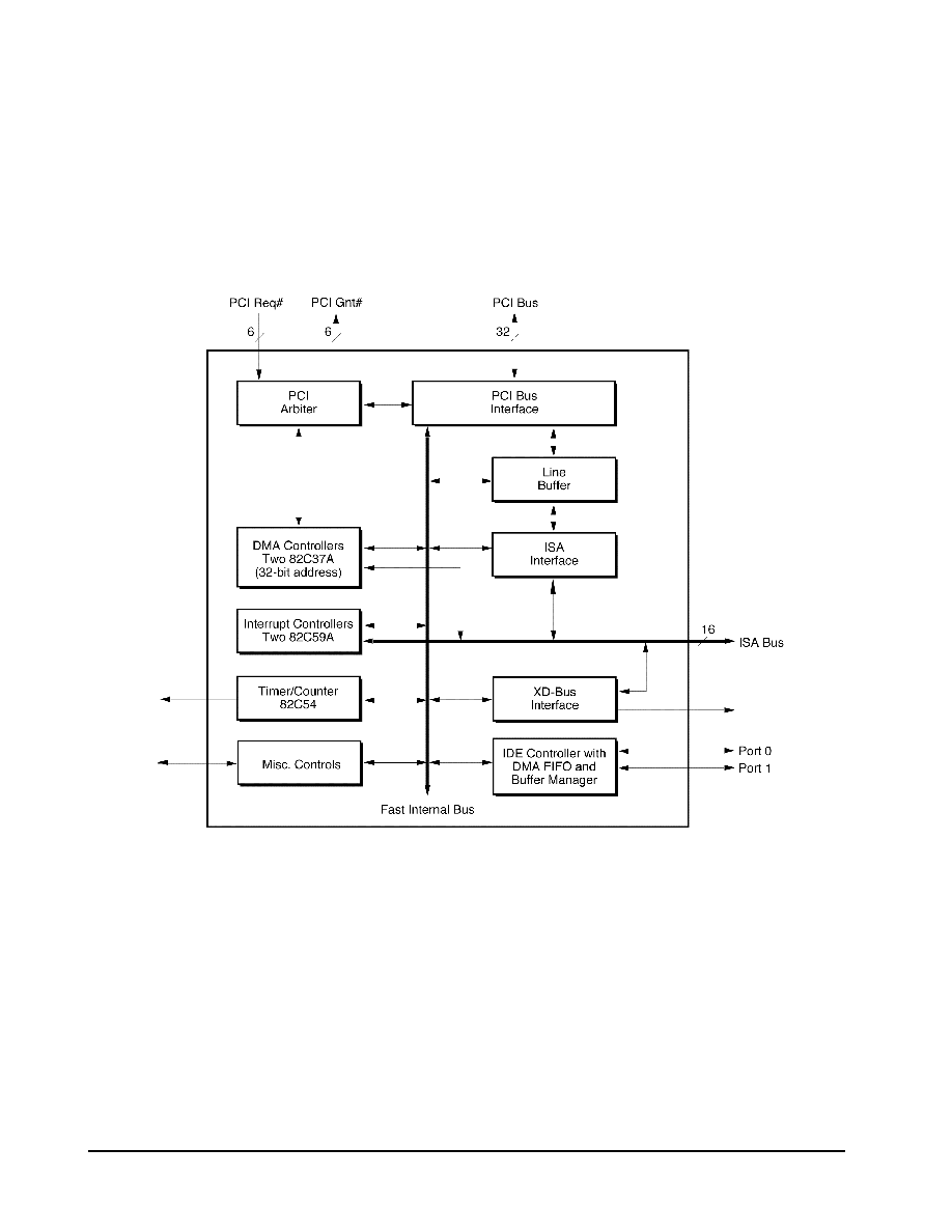
Figure 1-1. W83C553F Enhanced System I/O Controller Block Diagram

W83C553F General Information
WINBOND SYSTEMS LABORATORY
9
1.3 Stylistic Conventions Used in this Manual
The following stylistic conventions have been used throughout this manual:
� Signal names: Signals that are active at a low voltage level are indicated by a pound sign (#) after the
signal name. Signal names not followed by the # are active at the high voltage level.
� Least significant bits in words and words within memory spaces begin with zero (0). When a range is
given, the most significant bit is shown to the left and the least significant bit is shown to the right. For
example, AD[31:0].
� Hexadecimal numbers are given with the number in upper case followed by a lower case 'h'. For
example, " 8AFFh".
W83C553F Pin Descriptions
WINBOND SYSTEMS LABORATORY
10
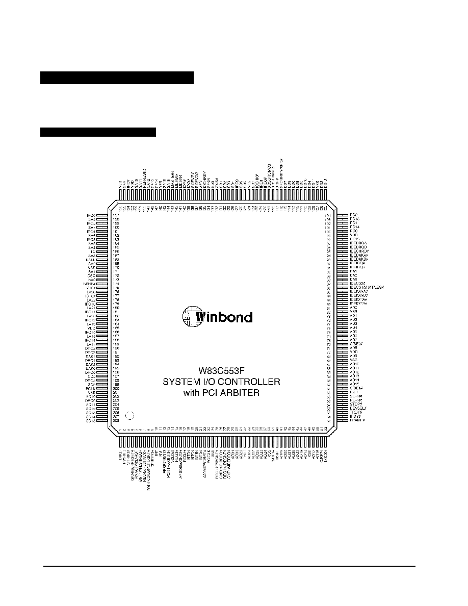
2.0 PIN DESCRIPTIONS
This chapter shows the pin diagrams, pins listed by pin number, device logic symbols, and describes each pin signal for the
W83C553F.
2.1 Pin Assignments
Figure 2-1. Pin Assignments for the W83C553F

W83C553F Pin Descriptions
WINBOND SYSTEMS LABORATORY
11
Table 2-1. W83C553F Pins Listed by Pin Number
1 DRQ7
2 PWRGD
3 INIT
4 IGNNE#/HRESET#
5 PMACT#/ISARST
6 GNT4#/FLSHREQ#
7 REQ4#/FLSHACK#
8 PWRPC/X86#/CPUGNT#
9 CPUREQ#
10 INT
11 NMI
12 FERR#/IRQ13
13 PCI5TH#/GNT3#
14 VDD
15 REQ3#
16 ARBDIS#/GNT2#
17 REQ2#
18 INTD#
19 INTC#
20 INTB#
21 INTA#
22 A20M#/PCIRST#
23 PCICLK
24 VSS
25 REQ0#/PIBGNT#
26 GNT0#/PIBREQ#
27 REQ1#/IDEGNT#
28 GNT1#/IDEREQ#
29 AD31
30 AD30
31 AD29
32 VDD
33 AD28
34 AD27
35 AD26
36 AD25
37 AD24
38 VSS
39 C/BE3#
40 IDSEL
41 AD23
42 AD22
43 AD21
44 AD20
45 VDD
46 AD19
47 AD18
48 VSS
49 AD17
50 AD16
51 C/BE2#
52 LOCK#
53 FRAME#
54 IRDY#
55 TRDY#
56 DEVSEL#
57 STOP#
58 PERR#
59 SERR#
60 PAR
61 C/BE1#
62 AD15
63 AD14
64 AD13
65 AD12
66 AD11
67 AD10
68 VSS
69 AD9
70 VDD
71 AD8
72 C/BE0#
73 AD7
74 AD6
75 AD5
76 AD4
77 AD3
78 AD2
79 AD1
80 VSS
81 AD0
82 IDEIORB#
83 IDEIORA#
84 IDEIOWB#
85 IDEIOWA#
86 IDECS1#/NAT/
LEG#
87 IDECS0#
88 DA2
89 DA0
90 DA1
91 IDEIRQB
92 IDEIRQA
93 IDEDAKB#
94 IDEDAKA#
95 IDECHRDY
96 IDEDRQB
97 IDEDRQA
98 DD15
99 VDD
100 DD0
101 DD14
102 DD1
103 DD13
104 DD2
105 DD12
106 DD3
107 VSS
108 DD11
109 DD4
110 DD10
111 DD5
112 DD9
113 DD6
114 DD8
115 DD7
116 SECURITY/XRD#
117 XOE#
118 XCS1/X8XCS
119 XCS0/ROMCS
120 IRQ8#
121 IRQ1
122 IOCHK#
123 SD7
124 VSS
125 SD6
126 SD5
127 IRQ9
128 SD4
129 SD3
130 SD2
131 SD1
132 ZWS#
133 SD0
134 SPKR
135 IOCHRDY
136 AEN
137 SMEMW#
138 SMEMR#
139 IOW#
140 IOR#
141 MEMR#
142 MEMW#
143 MASTER#
144 SA16
145 SA15
146 VSS
147 SA14
148 SA13
149 SA12
150 REFRESH#
151 SA11
152 SA10
153 VDD
154 IRQ7
155 SA9
156 VSS
157 IRQ6
158 SA8
159 IRQ5
160 SA7
161 IRQ4
162 SA6
163 IRQ3
164 SA5
165 SA4
166 TC
167 SA3
168 BALE
169 SA2
170 VSS
171 SA1
172 OSC
173 SA0
174 SBHE#
175 M16#
176 LA23
177 IO16#
178 LA22
179 IRQ10
180 LA21
181 IRQ11
182 LA20
183 IRQ12
184 LA19
185 VDD
186 IRQ15
187 LA18
188 IRQ14
189 LA17
190 DRQ2
191 DRQ3
192 DAK1
193 DRQ1
194 DAK2
195 DAK0
196 DRQ0
197 SD8
198 DRQ5
199 SD9
200 BCLK
201 VSS
202 SD10
203 DRQ6
204 SD11
205 SD12
206 SD13
207 SD14
208 SD15
W83C553F Pin Descriptions
WINBOND SYSTEMS LABORATORY
12
Note: Pins direction and assignment may not reflect exact pins , refers to exact pin description .
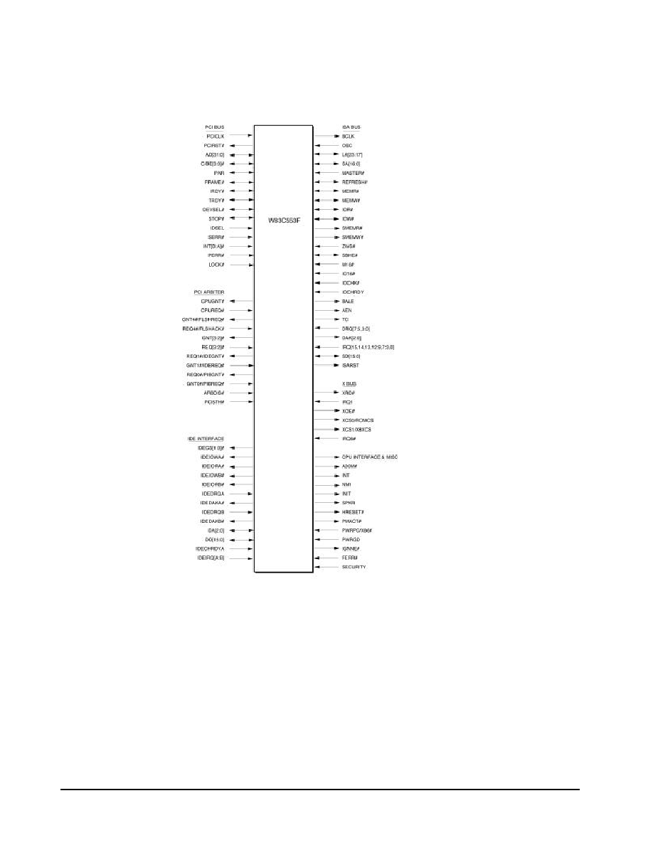
Figure 2-2. W83C553F Logic Symbol Diagram

W83C553F Pin Descriptions
WINBOND SYSTEMS LABORATORY
13
2.2 Pin Description
s
This section describes the location and function of each pin on the W83C553F. Note the following conventions used in the
tables:
� Where more than one pin is listed for a signal, the first pin number corresponds to the most significant
bit of the bus. For example, the Bus Command and Byte Enables bits 3 to 0 (C/BE[3:0]#) use pins 1,
12, 22, and 31.
� Active low is indicated by the pound (#) sign. For example, PCIRST# is active low.
�
Six strap pins are marked bold.

W83C553F Pin Descriptions
WINBOND SYSTEMS LABORATORY
14
Table 2-2. PCI Bus Signals
Pin Name
Pin #
Input/
Output
Description
PCICLK
23
Input
Clock. Provides timing for all transactions on the PCI bus. Also
divides down to generate BCLK.
A20M# /
PCIRST#
22
Output
Address Bit 20 Mask or PCI Reset. This multi-function pin
functions as Address Bit 20 Mask when the W83C553F is in x86
mode, as determined by pin 8 strapping after power-up. It functions
as PCI Reset when the W83C553F is in PowerPC mode. It is driven
for one millisecond duration after one of the following conditions:
- PWRGD active edge
- Hot Reset is set (port 92, bit 0)
- Reset Drive is set (Clock Divisor Register bit 3)
PCI Reset is equivalent to ISA Reset logically inverted.
AD[31:0]
29-31,33-37,41-
44, 46,47, 49,
50, 62-67,
69,71,73 -
79,81
Input/
Output
Address or Data. These bits are multiplexed on the same PCI pins.
A valid 32-bit address is available during the address phase with
FRAME# asserted. All subsequent cycles are the data phases.
C/BE[3:0]#
39, 51, 61,
72
Input/
Output
Bus Command and Byte Enables. These bits are multiplexed on the
same PCI pins. During the address phase of a transaction,
C/BE[3:0]# define the bus command. During the data phase,
C/BE[3:0]# are used for byte enables.
PAR
60
Input/
Output
Parity. Even parity across AD[31:0] and C/BE[3:0]#. PAR is valid
one clock after the address phase. For data phases, PAR is valid one
clock after either IRDY# is asserted on the write transaction, or
TRDY# is asserted on a read transaction. PAR remains valid until
one clock after the completion of the current phase. PAR is driven
only for read data phases, and checked during write data phases.

W83C553F Pin Descriptions
WINBOND SYSTEMS LABORATORY
15
Table 2-2 (Continued). PCI Bus Signals
Pin Name
Pin #
Input/
Output
Description
FRAME#
53
Input/
Output
Cycle Frame. Indicates the start and duration of an access. It is
asserted to indicate the start of a bus transaction; during which data
transfers continue. When FRAME# is de-asserted, the transaction is
in the final data phase.
PERR#
58
Input/
Output
PCI Parity Error.
IRDY#
54
Input/
Output
Initiator Ready. Indicates the initiating agent's ability to complete
the current transaction's data phase. It is used jointly with TRDY#.
During a write, it indicates that valid data is present on AD[31:0].
During a read cycle, it indicates the master is prepared to accept
data.
TRDY#
55
Input/
Output
Target Ready. Indicates the target's ability to complete the current
data phase of the transaction. It is used with IRDY#. During a read
cycle, it indicates that valid data is present on AD[31:0]. During a
write cycle, it indicates the target is prepared to accept data.
DEVSEL#
56
Input/
Output
Device Select. This signal is asserted by the W83C553F when it is
acting as a target in a transaction. It is an input when the W83C553F
is acting as the initiator of a transaction.
STOP#
57
Input/
Output
Stop. This is asserted to terminate the current transaction. It causes a
disconnect condition, limiting slave I/O cycles to one data transfer
since I/O burst transfers are not supported. During master cycles, it
indicates the target wants to terminate the cycle.
IDSEL
40
Input
Initialization Device Select. Chip select signal, used during PCI
configuration read and write cycles.
SERR#
59
Input/OD
System Error. The W83C553F monitors the SERR# pin to generate
an NMI if enabled.

W83C553F Pin Descriptions
WINBOND SYSTEMS LABORATORY
16
Table 2-2 (Continued). PCI Bus Signals
Pin Name
Pin #
Input/
Output
Description
INT[A:B]#
21-20
Input
PCI Interrupts. These PCI interrupts can be routed to the
programmable interrupt controller inside the W83C553F under
software control.
INT[C:D]#
19-18
Input/
OD
PCI Interrupts. These PCI interrupts can be routed to the
programmable interrupt controller inside the W83C553F under
software control.
LOCK#
52
Input
PCI Lock. LOCK# is used to indicate an atomic operation that may
require multiple transactions to complete.

W83C553F Pin Descriptions
WINBOND SYSTEMS LABORATORY
17
Table 2-3. PCI Arbiter Signals
Pin Name
Pin #
Input/
Output
Description
GNT0# /
PIBREQ#
26
Output
This is a multifunction pin. The W83C553F PCI-ISA bridge
(Function 0) asserts this signal to request the use of the PCI bus
when the on-chip PCI arbiter is disabled. This pin functions as
GNT0# when the on-chip PCI arbiter is enabled, allowing PCI
access to an external master.
REQ0# /
PIBGNT#
25
Input
This is a multifunction pin. An external arbiter asserts this signal to
grant the next PCI access to the PCI-ISA bridge (Function 0) when
the on-chip PCI arbiter is disabled. This pin functions as REQ0#
when the on-chip PCI arbiter is enabled.
GNT1# /
IDEREQ#
28
Output
This is a multifunction pin. The W83C553F IDE master (Function
1) asserts this signal to request the use of the PCI bus when the on-
chip PCI arbiter is disabled. This pin functions as GNT1# when the
on-chip PCI arbiter is enabled, allowing PCI access to an external
master.
REQ1# /
IDEGNT#
27
Input
This is a multifunction pin. An external arbiter asserts this signal to
grant the next PCI access to the IDE master when the on-chip PCI
arbiter is disabled. This pin functions as REQ1# when the on-chip
PCI arbiter is enabled.
ARBDIS# /
GNT2#
16
Input/
Output
When the on-chip PCI arbiter is enabled, it uses this pin to grant the
next PCI access. If a 2.2k Ohm resistor straps this pin to ground,
the PCI arbiter is disabled after power-up. This overrides the
strapping of PCI5TH# on pin 13.
REQ2#
17
Input
When the on-chip PCI arbiter is enabled, external PCI masters use
this pin to request access to the PCI bus.

W83C553F Pin Descriptions
WINBOND SYSTEMS LABORATORY
18
Table 2-3 (continued). PCI Arbiter Signals
Pin Name
Pin #
Input/
Output
Description
PCI5TH# /
GNT3#
13
Input/
Output
When the on-chip PCI arbiter is enabled, GNT3# behaves as a
normal PCI grant output.
If a 2.2K ohm resistor straps this pin to ground, pin 6 and 7 function
as GNT4# and REQ4# after power-up. If this pin is weakly
strapped to VCC, pin 6 and 7 function as FLSHREQ# and
FLSHACK# after power-up. The PCI5TH# function is overridden
by the ARBDIS# function (i.e., if the on-chip PCI arbiter is
disabled, pin 6 and 7 function as FLSHREQ# and FLSHACK# no
matter how PCI5TH# is strapped.)
REQ3#
15
Input
When the on-chip PCI arbiter is enabled, REQ3# behaves as a
normal PCI request input.
GNT4# /
FLSHREQ#
6
Output
This is a multifunction pin which is alternately used to request
flushing all buffers or granting PCI access to an external master.
REQ4# /
FLSHACK#
7
Input
This is a multifunction pin which is alternately used as flush
acknowledge or as a PCI access request input.
PWRPC/X86#
/
CPUGNT#
8
Input/
Output
This multifunction pin is sampled by the W83C553F, following the
PWRGD active edge. If a 2.2K ohm resistor is weakly pulling this
pin to VCC at this time, the W83C553F is in PowerPC mode. If a
weak pull down resistor is connected to ground, the chip is in x86
mode.
When the PCI arbiter within the W83C553F is enabled (pin 16
Arbdis#/GNT2# is weakly pulled high), this pin functions as the
CPU Grant output which allows the system CPU-to-PCI bridge to
have access to PCI.
CPUREQ#
9
Input
This input allows the system CPU to request access to the PCI bus
in systems with the PCI arbiter within the W83C553F enabled.

W83C553F Pin Descriptions
WINBOND SYSTEMS LABORATORY
19
Table 2-4. IDE Interface Bus Signals
Pin Name
Pin #
Input/
Output
Description
IDECS0#
87
Output
Drive Chip Select 0. This signal is decoded from the AD bus to
select both primary and secondary IDE Port Command Block
Registers.
IDECS1#/
NAT/LEG#
86
Input/
Output
Drive Chip Select 1. This signal is decoded from the AD bus to
select both primary and secondary IDE Port Auxiliary Registers.
Native or Legacy Mode Select. During reset, this pin is sampled as
an input to set the Native or Legacy mode of the bus master IDE
controller (Function 1). A high selects Native mode and a low
selects Legacy mode.
IDEIOWA#
85
Output
Drive I/O Write A. This signal is used jointly with IDECS0# and
IDECS1#. The rising edge of IDEIOWA# latches data into the
primary port IDE device.
IDEIORA#
83
Output
Drive I/O Read A. This signal is used jointly with IDECS0# and
IDECS1#. The falling edge of IDEIORA# enables data from the
primary port IDE device. The data is latched internally on the rising
edge of IDEIORA#.
IDEIOWB#
84
Output
Drive I/O Write B. This signal is used jointly with IDECS0# and
IDECS1#. The rising edge of IDEIOWB# latches data into the
secondary port IDE device.
IDEIORB#
82
Output
Drive I/O Read B. This signal is used jointly with IDECS0# and
IDECS1#. The falling edge of the IDEIORB# enables data from the
secondary port IDE device. The data is latched internally on the
rising edge of IDEIORB#.

W83C553F Pin Descriptions
WINBOND SYSTEMS LABORATORY
20
Table 2-4 (continued). IDE Interface Bus Signals
Pin Name
Pin #
Input/
Output
Description
IDEDRQA
97
Input
DMA Request A. This signal is the primary port DMA handshake
from the IDE device. When asserted, it indicates a data transfer is
requested.
IDEDAKA#
94
Output
DMA Acknowledge A. This is the primary port DMA handshake to
the IDE device. When asserted, it indicates a data transfer can be
executed.
IDEDRQB
96
Input
DMA Request B. This is the secondary port DMA handshake from
the IDE device. When asserted, it indicates a data transfer is
requested.
IDEDAKB#
93
Output
DMA Acknowledge B. This is the secondary port DMA handshake
to the IDE device. When asserted, it indicates a data transfer can be
executed.
DA[2:0]
88,90,89
Output
IDE Drive Address.
DD[15:0]
98,101,103,
105,108,
110,112,
114,115,
113,111,
109,106,
104,102,
100
Input/
Output
IDE Drive Data. 16-bit bi-directional bus.
IDECHRDY
95
Input
IDE I/O Channel Ready. When IDECHRDY is negated, the current
cycle will be extended. This input is connected to the primary port,
and can also be connected to the secondary port.
IDEIRQB
91
Input
IDE IRQ B. Secondary port interrupt request.
IDEIRQA
92
Input
IDE IRQ A. Primary port interrupt request.

W83C553F Pin Descriptions
WINBOND SYSTEMS LABORATORY
21
Table 2-5. ISA Bus Signals
Pin Name
Pin #
Input/
Output
Description
BCLK
200
Output
ISA Bus Clock.
OSC
172
Input
Oscillator. 14 MHz input for generating the internal timer clock.
LA[23:17]
176,178,
180,182,
184,187,
189
Input/
Output
Latchable Address. The current bus owner drives LA[23:17] to
provide 16M of memory space.
SA[16:0]
144,145,
147-149,
151,152,
155,158,
160,162,
164,165,
167,169,
171,173
Input/
Output
System Address. SA[16:0] provides the 17 least significant address
bits for memory accesses and SA[15:0] provides the entire 16
address bits for I/O accesses.
MASTER#
143
Input
ISA Master. Master control signal from the ISA bus.
REFRESH#
150
Input/
Output
ISA DRAM Refresh Control. This pin is an open drain output and
allows other masters to initiate refresh requests.
MEMR#
141
Input/
Output
Memory Read. Acts as an output during PCI master and DMA
cycles and as an input during ISA master cycles.
MEMW#
142
Input/
Output
Memory Write. Acts as an output during PCI master and DMA
cycles and as an input during ISA master cycles.

W83C553F Pin Descriptions
WINBOND SYSTEMS LABORATORY
22
Table 2-5 (Continued). ISA Bus Signals
Pin Name
Pin #
Input/
Output
Description
IOR#
140
Input/
Output
I/O Read. Act as an output during PCI master and DMA cycles and
as an input during ISA master cycles.
IOW#
139
Input/
Output
I/O Write. Act as an output during PCI master and DMA cycles and
as input during ISA master cycles.
SMEMR#
138
Output
Memory Read To Address Below 1M. An external pull-up resistor
is required.
SMEMW#
137
Output
Memory Write To Address Below 1M. An external pull-up resistor
is required.
ZWS#
132
Input
Zero Wait State. This signal is used by ISA slaves to terminate a
transfer cycle before the default ready counter expires.
SBHE#
174
Input/
Output
System Byte High Enable. SBHE# is asserted to indicate that data
is being transferred on SD[15:8].
M16#
175
Input/
Output
Memory Cycle 16-Bit Select. This signal is used by memory slaves
to indicate 16-bit transfer capability.
IO16#
177
Input
I/O Cycle 16-Bit Select. This signal is used by I/O slaves to
indicate 16-bit transfer capability.
IOCHK#
122
Input
I/O Channel Check. This assertion of this signal indicates an error
has occurred.

W83C553F Pin Descriptions
WINBOND SYSTEMS LABORATORY
23
Table 2-5 (Continued). ISA Bus Signals
Pin Name
Pin #
Input/
Output
Description
IOCHRDY
135
Input/
Output
I/O Channel Ready. This signal is used by ISA slaves to extend the
transfer cycle beyond the default ready timer expiration.
BALE
168
Output
Bus Address Latch Enable. This signal indicates that a valid
address is on the bus.
AEN
136
Output
Address Enable. AEN is asserted during DMA cycles to prevent
I/O devices from misinterpreting the cycle as a valid I/O cycle.
TC
166
Output
Termination Count. This signal is asserted to indicate that a DMA
channel's word count has reached terminal count.
DRQ[7:5, 3:0]
1,203,198,
191,190,
193,196
Input
DMA Request. DMA service request from the DMA controllers.
DAK[2:0]
194,192,
195
Output
Encoded DMA Acknowledge. The channel number of the
arbitration winner is encoded in binary. An external decoder is
required to generate DACK[7:5, 3:0]#. The inactive value is 100b.
IRQ[15, 14, 12:9,
7:3]
186,188,
183,181,
179,127,
154,157,
159,161,
163
Input
Interrupt Request.

W83C553F Pin Descriptions
WINBOND SYSTEMS LABORATORY
24
Table 2-5 (Continued). ISA Bus Signals
Pin Name
Pin #
Input/
Output
Description
PMACT# /
ISARST
5
Output
This multi-function pin functions as ISA Reset when the
W83C553F is in PowerPC mode, as determined by pin 8 strapping
after power-up. It is driven for one millisecond duration after one of
the following conditions:
- PWRGD active edge
- Hot Reset bit set (port 92, bit 0)
- Reset Drive bit set (Clock Divisor Register bit 3)
ISA Reset is the inverted logical equivalent of PCI Reset.
When the W83C553F is in x86 mode, this pin functions as Power
Management Active. It is the output signal to the CPU bridge
which indicates the system activity status by becoming active when
a break event has occurred. Break events are programmed into PCI
Configuration Registers index 60h - 63h.
SD[15:0]
208-204,
202,199,
197,123,
125,126,
128-131,
133
Input /
Output
Bidirectional Data Bus.

W83C553F Pin Descriptions
WINBOND SYSTEMS LABORATORY
25
Table 2-6. X Bus Signals
Pin Name
Pin #
Input/
Output
Description
SECURITY /
XRD#
116
Output/
Input
X Bus Read. When active "0", data flows from XD to SD. When
the W83C553F is in PowerPC mode, this pin is sampled after reset
and its value is reflected in bit 2 of the Port 92 register (see page
107).
IRQ1
121
Input
Keyboard Controller Interrupt.
IRQ8#
120
Input
Real Time Clock Interrupt.
XOE#
117
Output/
Input
X Bus Buffer Enable. This signal enables an external X-bus buffer
whenever an X-bus device is decoded. This pin is a strap pin, needs
a 2.2k Ohm resistor pull up, otherwise will be in test mode.
XCS0/
ROMCS
119
Output
This is a multi-function pin. When the W83C553F is in PowerPC
mode, this pin functions as the chip select for an external ROM,
using default ISA memory cycle timing. When the W83C553F is in
x86 mode, this pin functions as the lower bit of the X-bus Address.
XCS1/X8XCS
118
Output
This is a multi-function pin. When the W83C553F is in PowerPC
mode, this pin functions as the chip select for ports in the 800h-
8FFh I/O address range. When the W83C553F is in x86 mode, this
pin functions as the upper bit of the X-bus Address. In x86 mode,
an external decoder is required to decode the chip selects for X-bus
devices:
XCS[1:0] Device
00 Idle
01 RTC Address Latch
10 RTC Data Port
11 ROM/BIOS or Keyboard Controller

W83C553F Pin Descriptions
WINBOND SYSTEMS LABORATORY
26
Table 2-7. CPU Interface and Miscellaneous Signals
Pin Name
Pin #
Input/
Output
Description
INT
10
Output
Interrupt. Interrupt signal from the W83C553F interrupt controller to the
CPU.
NMI
11
Output
Non-Maskable Interrupt.
INIT
3
Output
It functions as Initialize CPU/Software Reset (INIT) when the W83C553F
is in x86 mode, as determined by pin 8 strapping after reset. INIT is
asserted for four PCI clocks following one of these events:
- Hot Reset bit set (port 92, bit 0)
- CPU Shutdown Cycle
- keyboard Reset Emulation bit is set (bit 1, Index 4E)
SPKR
134
Output
Speaker Data. This output drives an externally buffered speaker.
PWRGD
2
Input
Power good signal from the power supply. This signal is used to generate
other reset signals to reset the system.
FERR#/IRQ13
12
Input
This multi-function pin's default function is Interrupt Request 13 (IRQ13).
The Numerical Co-processor Error (FERR#) function may be enabled by a
bit in the Function 0 PCI Configuration Space AT System Control Register
(Index 4Eh, bit 4).
IGNNE# /
HRESET#
4
Output
This multi-function pin functions as Ignore Numeric Error (IGNNE#)
when the W83C553F is in x86 mode as determined by pin 8 strapping after
reset. It functions as HRESET# when the W83C553F is in PowerPC
mode. For connection to the PowerPC, HRESET# is asserted for a
duration of one millisecond after one of the following events:
- PWRGD active edge
- Hot Reset bit set (port 92, bit 0)
- CPU Shutdown Cycle
- Keyboard Reset Emulation bit is set (bit 1, Index 4E)

W83C553F Pin Descriptions
WINBOND SYSTEMS LABORATORY
27
Table 2-8. Power and Ground Signals
Pin Name
Pin #
Input/
Output
Description
VSS
24,38,48,
68,80,
107,124,
146,156,
170,201
-
These 11 pins are connected to the power supply ground. All VSS
pins must be connected for proper device operation.
VDD
14,32,45,
70,99,153,185
-
These 7 pins are connected to the power supply +5V. All VDD pins
must be connected for proper device operation.

W83C553F Electrical Specifications
WINBOND SYSTEMS LABORATORY
28
3.0 SYSTEM ARCHITECTURE
3.1 Overview
The W83C553F is a multi-function PCI device. "Function 0" is the PCI-to-ISA bridge logic; "Function 1" is the bus master
IDE controller. Each function has its own separate PCI configuration space and I/O register space.
The W83C553F's bus hierarchy is designed to provide concurrency of operations performed on all buses simultaneously and
is structured as follows:
� PCI Bus is primary I/O bus
� ISA Bus is secondary I/O bus
The W83C553F accepts cycles from the PCI bus and translates them onto the ISA bus. It also requests the PCI master bridge
to generate PCI cycles on behalf of IDE DMA or an ISA master. The ISA bus interface thus contains a standard ISA Bus
Controller and data buffering logic. ISA control includes ISA command generation, I/O recovery control, wait-state
insertion, and data buffer routing. Five ISA slots can be supported without external buffering circuitry.
The W83C553F initiates and performs standard ISA bus refreshing. The integrated controller generates the command and
refresh address to the ISA bus. Since an ISA refresh is transparent to the PCI bus and the DMA cycle, an arbiter resolves any
conflicts among PCI, refresh, and DMA cycles.
IDE data transfers are executed with two specific protocols. The standard protocol is to execute PIO cycles on the PCI bus
and the dual IDE interfaces. An enhanced protocol is supported, allowing the W83C553F to transfer data across the PCI bus
as a bus master directly to/from memory, and across the dual IDE interfaces with single or multiword DMA cycles. This
protocol minimizes CPU overhead while maximizing the PCI bus bandwidth.
All IDE PIO protocol data transfers (8-bit, 16-bit and 32-bit) are automatically detected and supported. Read ahead can be
enabled for each individual device for 16-bit and 32-bit I/O read operations. This allows the controller to execute additional
IDE read cycles while the host is completing the previous memory write. Posted writes can be enabled for each individual
device for 16-bit and 32-bit I/O write operations which allow the IDE controller to complete the present write cycle while the
host executes the next system memory read operation maximizing the disk sub-system performance while reducing system
overhead.
Bus Master data/command transfers are supported as defined in the proposed PCI "Programming Interface for Bus Master IDE
Controller" specification Rev. 1.0 (SFF8038i). This allows the system microprocessor to be freed from the task of manually
transferring data between the IDE controller and the system memory as is required by the standard PIO protocol. In a
multitasking environment, the system CPU can perform other tasks with the maximum PCI bus bandwidth available while data
transfers are executed by the W83C553F.

W83C553F Electrical Specifications
WINBOND SYSTEMS LABORATORY
29
The IDE interface is fully ANSI CAM compliant to the ATA Revision 3.0 and the ATA-2 specifications. Each storage
device on the two ports is individually programmable to select the desired command on and off times to support ATA defined
PIO MODES 0 through 2 and Multiword DMA MODE 0. Also supported are SFF PIO MODES 3, 4 and 5 (proposed) and
Multiword DMA MODES 1 and 2.
The devices supported are ATA compliant hard disks, tape drives, and CD ROMs. The W83C553F is compliant with the
emerging ATAPI Specification.
Two interrupt controllers can handle a total of 15 interrupt channels. IRQ0 is internally connected to OUT0, of the 82C54
counter/timer. Usually an interrupt is generated by the rising edge of IRQ. IRQ8 and IRQ13, however, are fixed to trigger
on the falling edge for direct connection to the real time clock interrupt or Pentium CPU floating point error signal. RX
4D0h and RX4D1h can be programmed to change the IRQs from edge sensitive to level sensitive interrupts. All external
IRQ lines are not internally pulled-up. I/O port and channel definition matches the IBM PC/AT requirement.
Types A, B, F DMA are supported by the W83C553F. Two integrated 82C37A DMA controllers each generate memory
addresses and control signals to transfer information between a peripheral device and memory, without CPU intervention.
Four DMA channels permit 8-bit peripheral device data transfers. Three channels permit 16-bit peripheral device data
transfers. During a DMA or master cycle, the CPU is held and the W83C553F takes control. Both DMA controllers support
scatter/gather transfer capability on all channels and 32-bit addressing.
The W83C553F has two basic operational states: reset and active. The reset state brings all internal logic to a known state,
and configures some chip features. The active state is the normal operating state that allows software to perform chip
configuration, access to the PCI and ISA register sets, and accessing of up to four IDE devices.
3.2 Active State
When active, the W83C553F will monitor all PCI bus cycles and respond to configuration and I/O cycles. The W83C553F
will always respond to configuration cycles when properly addressed but will always respond to I/O cycles, as indicated in
the internal configuration registers.
Configuration cycles are executed anytime the W83C553F IDSEL pin is asserted, a valid command is detected, and AD[1:0]
are "0" during the address phase. Configuration cycles are executed to program the W83C553F internal configuration
register sets. I/O cycles will only be executed when enabled as indicated in the configuration registers. I/O cycles are used to
transfer command/status and data to/from the IDE devices, as well as to program the bus master register set.

W83C553F Electrical Specifications
WINBOND SYSTEMS LABORATORY
30
Four basic data paths are provided. One provides the timing and control functions for 8-bit I/O cycles that communicate
control/status information with the IDE devices. A second data path provides the timing and control functions for 16-bit and
32-bit I/O cycles that are used to transfer data to/from the IDE drives with the PIO protocol. The third is used to access the
internal Configuration and Bus Master IDE Register set. The fourth data path is used for the bus master data transfer
protocol. A block of logic is used to interface to the PCI bus as well as separate 8-bit from 16/32-bit cycles and provide bus
master support. A separate block of logic is used to control the IDE interface and timing as well as control the packing and
unpacking of the data between the IDE buffer logic and the PCI buffer logic.
3.3 Bus Structures
Table 3-1. Address and Data Paths for Basic Cycles
Cycle
Address Bus Path
Data Bus Path
ISA-to-PCI data read
PCI address/data->W83C553F
->Latched & ISA addressing
ISA data->W83C553F->PCI address/data
PCI-to-ISA data write
PCI address/data->W83C553F
->Latched & ISA addressing
PCI address/data->W83C553F
->ISA data
DMA read
W83C553F->PCI address/data, W83C553F-
>Latched & ISA address
PCI address/data->W83C553F
->ISA data
DMA write
W83C553F->PCI address/data, W83C553F-
>Latched & ISA address
ISA data->W83C553F->PCI address/data
ISA refresh
W83C553F->ISA address

W83C553F Electrical Specifications
WINBOND SYSTEMS LABORATORY
31
3.4 PCI-to-ISA Bridge
The W83C553F PCI System I/O provides the PCI bus interface functions. It contains both PCI master and slave bus
bridging. When PIBGNT# is asserted, the master bridge translates an ISA master or DMA cycle to the PCI bus, based on the
ISA Address Decoder status. When PIBGNT# is de-asserted, the slave bridge accepts these cycles, initiated from the PCI
bus, and targeted to the W83C553F's internal registers or ISA bus. The PCI Address Decoder supports the slave bridge in
processing the PCI master initiated cycles. The cycles are then forwarded to the ISA bus interface for translation onto the
ISA bus.
As a PCI slave, the W83C553F responds to both I/O and memory transactions. It always target-terminates after the first data
phase of a bursting cycle. It also converts a single interrupt acknowledge cycle into two cycles for the two internal 82C59s.
The W83C553F functions as the subtractive decoder in a PCI/ISA system by accepting all accesses not positively decoded by
some other device. This function only applies to the low 64 K I/O or low 16 M memory accesses.
The W83C553F positively decodes I/O addresses for internal registers by asserting DEVSEL# on the medium timing. In the
x86 mode, the keyboard controller and RTC are subtractively decoded.
As long as PIBGNT# is asserted, the PCI master bridge, on behalf of DMA devices or ISA Masters, drives the PCI
address/data, C/BE[3:0]# and PAR signals. When MEMR# or MEMW# is asserted, the W83C553F sends FRAME# and
IRDY# to the PCI bus if the targeted memory is not on the ISA side. Addresses and commands are valid during the address
phase, while PAR is asserted one clock later. The W83C553F always activates FRAME# for 2 PCLKs because it does not
conduct bursting cycles for PCI-to-ISA reads or writes.
The ISA Address Decoder determines the destination of the ISA master or DMA devices. It provides the following options,
as defined in Registers 48h to 4Bh:
� Memory space 0 - 512KB
� Memory space 512 KB - 640 KB
� Video Buffer memory space 640 KB - 768 KB
� Expansion ROM memory space 768 KB - 896 KB, in eight 16 KB sections
� Lower BIOS memory space 896 KB - 960 KB
� Memory space within 1 MB - x MB - 16 MB. Not accessible to the PCI bus.
� Memory space less than 16 MB automatically forwards to the PCI.
3.5 PCI Bus Cycles
The PCI bus cycle can be split into two phases, the address phase and the data phase. The address phase of a PCI cycle is
defined as the first rising clock edge when FRAME# is asserted. On this clock edge, C/BE[3:0]# contains the bus command
that defines the PCI bus cycle, AD [31:0] contains a valid address, and IDSEL will be stable and valid if it is a configuration
cycle. All subsequent clocks comprise the data phase until the cycle is complete. If this cycle is claimed, DEVSEL# will be
asserted.

W83C553F Electrical Specifications
WINBOND SYSTEMS LABORATORY
32
The next rising clock edge identifies the beginning of the data phase. Address parity is valid and will be checked or ignored
depending on the state of the SE bit of the Device Control Register. The data phase can last one or more clock cycles. Data
will be transferred on the rising clock edge when both IRDY# and TRDY# are asserted. Data parity will be generated (slave
I/O read or bus master memory write cycle) or checked (slave I/O write or bus master memory read cycle) on the next
rising clock edge. The W83C553F will report data parity errors on slave I/O write cycles it claims (by the assertion of
DEVSEL#) and bus master memory write cycles via the PERR# signal when enabled.
Normally for I/O cycles FRAME# will be de-asserted when IRDY# is asserted to signify that this is the last data transfer of
the data phase. STOP# will also be asserted with TRDY# to prevent I/O bursting. Multiple data phases (data bursting) are
supported when operating as a bus master.
Table 3-2 PCI Bus Cycles
C/BE[3:0]#
PCI Bus Cycle
Slave Mode
Master Mode
0 0 0 0
0 0 0 1
0 0 1 0
0 0 1 1
0 1 0 0
0 1 0 1
0 1 1 0
0 1 1 1
1 0 0 0
1 0 0 1
1 0 1 0
1 0 1 1
1 1 0 0
1 1 0 1
1 1 1 0
1 1 1 1
Interrupt Acknowledge
Special Cycle
I/O Read
I/O Write
Reserved
Reserved
Memory Read
Memory Write
Reserved
Reserved
Configuration Read
Configuration Write
Memory Read Multiple
Dual Address Cycle
Memory Read Line
Memory Write and Invalidate
Supported
Supported
Supported
Supported
Ignored
Ignored
Supported
Supported
Ignored
Ignored
Supported
Supported
Supported (aliased to Memory Read)
Ignored
Supported (aliased to Memory Read)
Supported (aliased to Memory Write)
Not Generated
Not Generated
Not Generated
Not Generated
Not Generated
Not Generated
Supported
Supported
Not Generated
Not Generated
Not Generated
Not Generated
Supported
Not Generated
Supported
Supported
W83C553F Electrical Specifications
WINBOND SYSTEMS LABORATORY
33
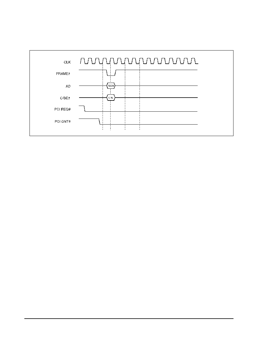
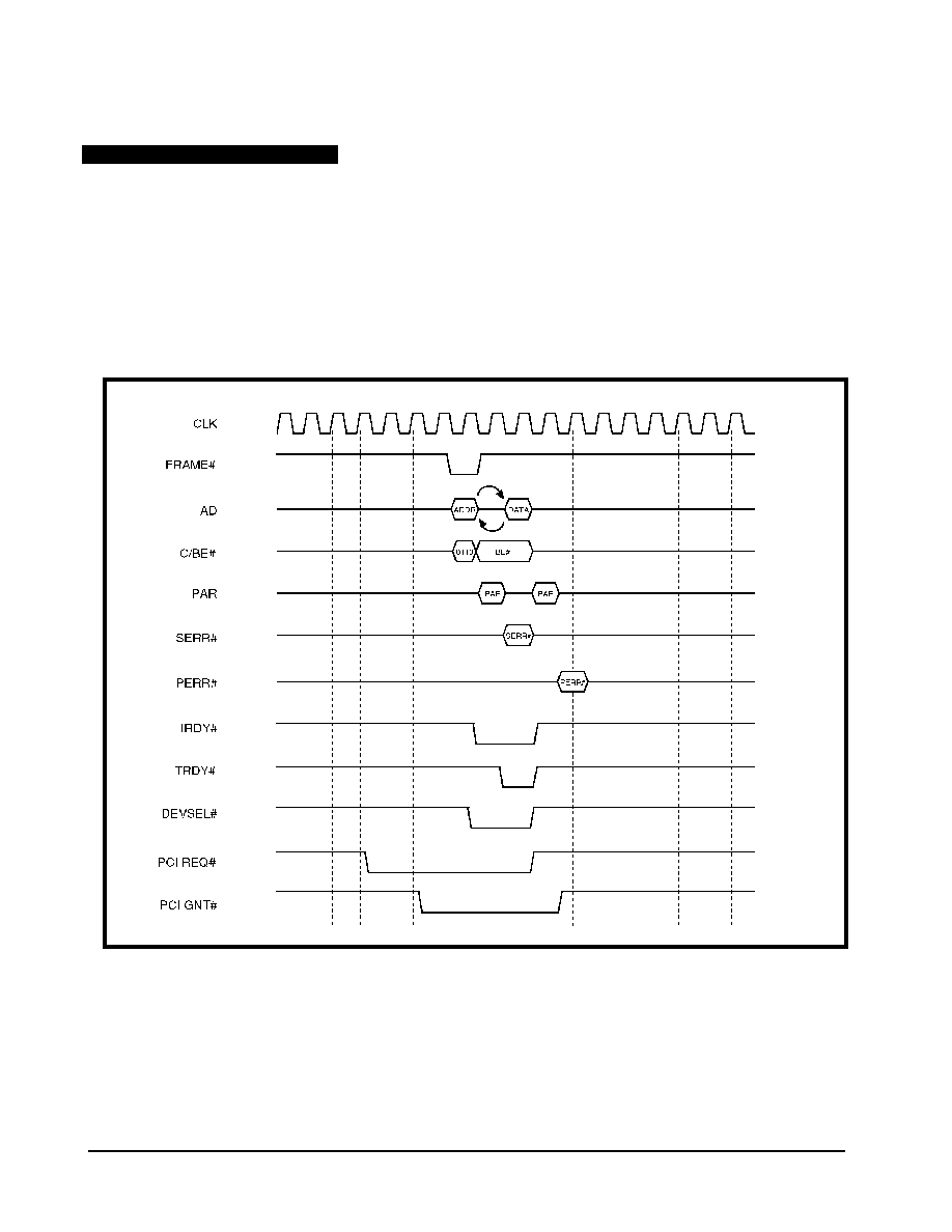
Refer to Figure 3-1. Bus acquisition timing cycles are defined by the C/BE[3:0]# command lines during the address (AD)
phase of each PCI cycle.
Figure 3-1. Bus Acquisition Timing
W83C553F Electrical Specifications
WINBOND SYSTEMS LABORATORY
34
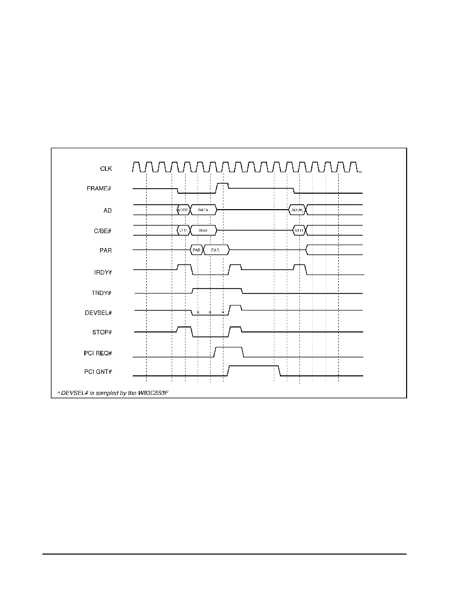
3.6 PCI I/O Read Cycle
Bursting is not supported by the W83C553F for I/O cycles, so a target disconnect will be executed after the first data transfer
on all I/O Read commands to prevent multiple I/O data phases.
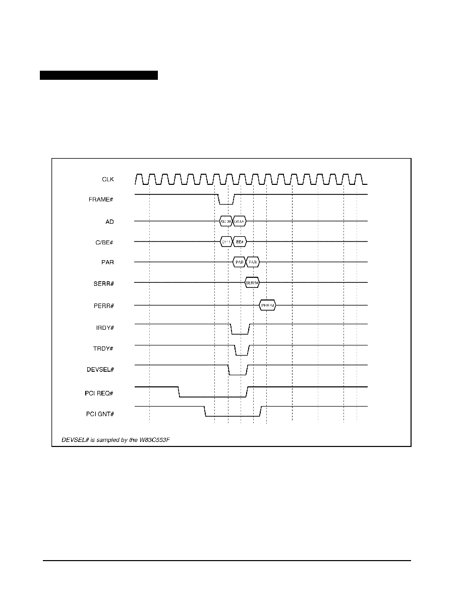
Refer to Figure 3-2. The Slave I/O Read command (C/BE[3:0]# = 2h during address phase) is used by the processor to read
the W83C553F internal bus master registers, IDE device, and ISA registers or X-bus registers. It is a single, non-burst, 8, 16
or 32-bit transfer cycle, initiated by the CPU. It is a fixed duration, i.e. the W83C553F will assert TRDY# on the 4th bus
cycle of the transfer when accessing the internal bus master registers. It will have a variable duration when accessing an IDE
device or ISA register.
Figure 3-2. Slave I/O Read Timing
W83C553F Electrical Specifications
WINBOND SYSTEMS LABORATORY
35
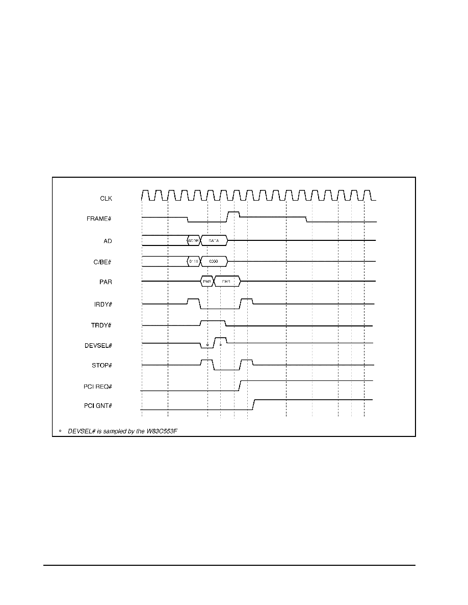
3.7 PCI I/O Write Cycle
Bursting is not supported by the W83C553F for I/O cycles, so a target disconnect will be executed after the first data transfer
on all I/O Write commands to prevent multiple I/O data phases.
Refer to Figure 3-3. The Slave I/O Write command (C/BE[3:0]# = 3h during address phase) is used by the processor to
write the W83C553F internal bus master registers, IDE device, and ISA registers or X-bus registers. It is a single, non-burst,
8, 16 or 32-bit transfer cycle, initiated by the CPU. It is a fixed duration, i.e. the W83C553F will assert TRDY# on the 4th
bus cycle of the transfer when accessing the internal bus master registers. It will have a variable duration when accessing an
IDE device or ISA register.
Figure 3-3. Slave I/O Write Timing
W83C553F Electrical Specifications
WINBOND SYSTEMS LABORATORY
36
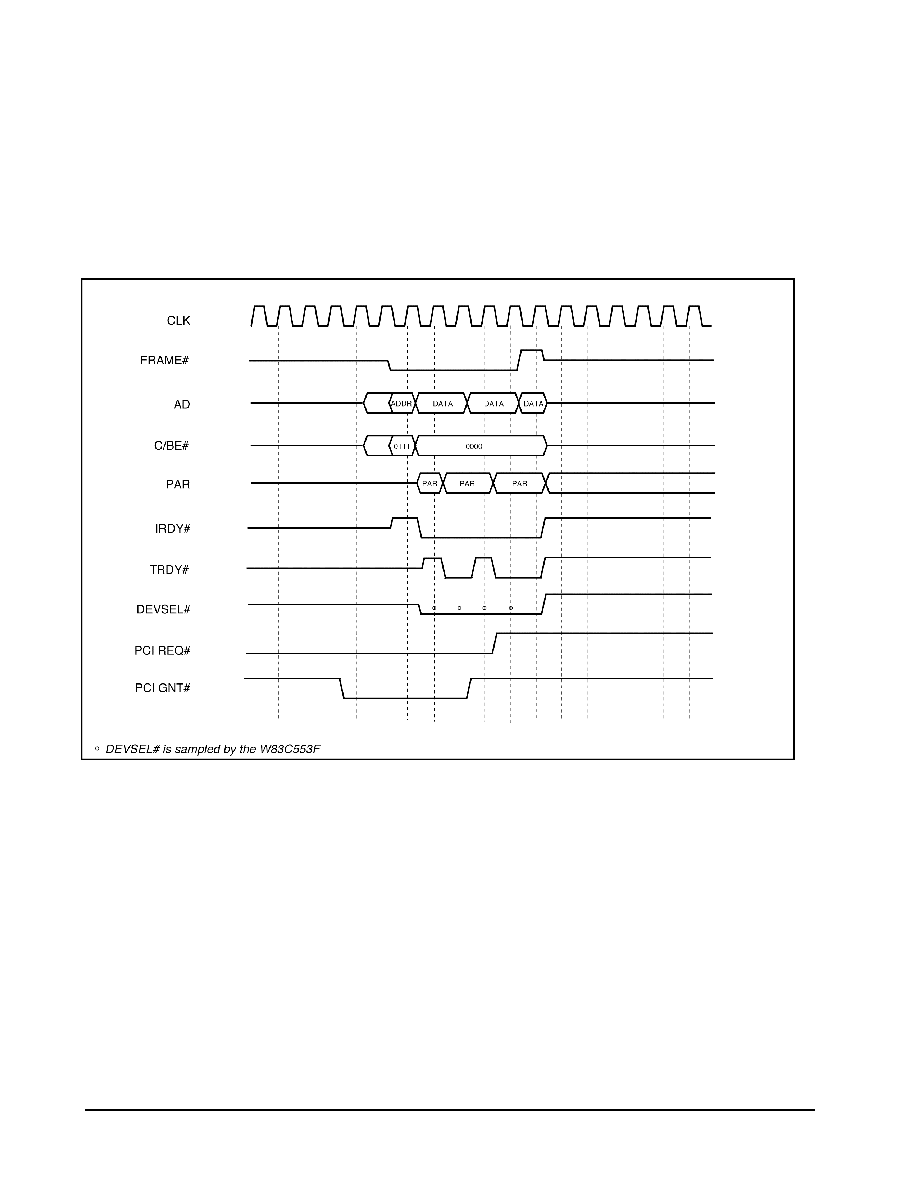
3.8 PCI Configuration Read Cycle
The Configuration Read command (C/BE[3:0]# = Ah during address phase) is used in slave mode to read the configuration
registers. 8-bit, 16-bit, 24-bit and 32-bit accesses are supported when the IDSEL is asserted and AD[1:0] are 00. The PCI
controller will respond to all Configuration Read cycles, even for bytes not used. A value of 00h will be read for each invalid
byte selected in the configuration address space. During the PCI address phase AD[7:2] define the DWORD accessed, while
the byte enables (C/BE[3:0]#) address the byte(s) within each DWORD.
Refer to Figure 3-4. The Slave Configuration Read command cycle is used by the host processor to read the PCI
configuration space in the W83C553F. This provides the processor with device information. It is a single, non-burst, 8, 16
or 32-bit transfer, of fixed duration, i.e. the W83C553F will assert TRDY# on the 4th bus cycle of the transfer.
Figure 3-4. Slave Configuration Read Timing
W83C553F Electrical Specifications
WINBOND SYSTEMS LABORATORY
37
3.9 PCI Configuration Write Cycle
The Configuration Write command (C/BE[3:0]# = Bh during address phase) is used in slave mode to write to the
configuration registers. 8-bit, 16-bit, 24-bit and 32-bit accesses are supported when the IDSEL is asserted and AD[1:0] are
00. The PCI controller will respond to all Configuration write cycles, even for bytes not used. During the PCI address phase
AD[7:2] define the DWORD accessed, while the byte enables (C/BE[3:0]#) address the byte(s) within each DWORD.
Refer to Figure 3-5. The Slave Configuration Write command cycle is used by the host processor to write the PCI
configuration space in the W83C553F. This permits the processor to control basic W83C553F activity, such as
enable/disable, change I/O location, etc. It is a single, non-burst, 8, 16 or 32-bit transfer, of fixed duration, i.e. the
W83C553F will assert TRDY# on the 4th bus cycle of the transfer.
Figure 3-5. Slave Configuration Write Timing
W83C553F Electrical Specifications
WINBOND SYSTEMS LABORATORY
38
3.10 PCI Memory Read
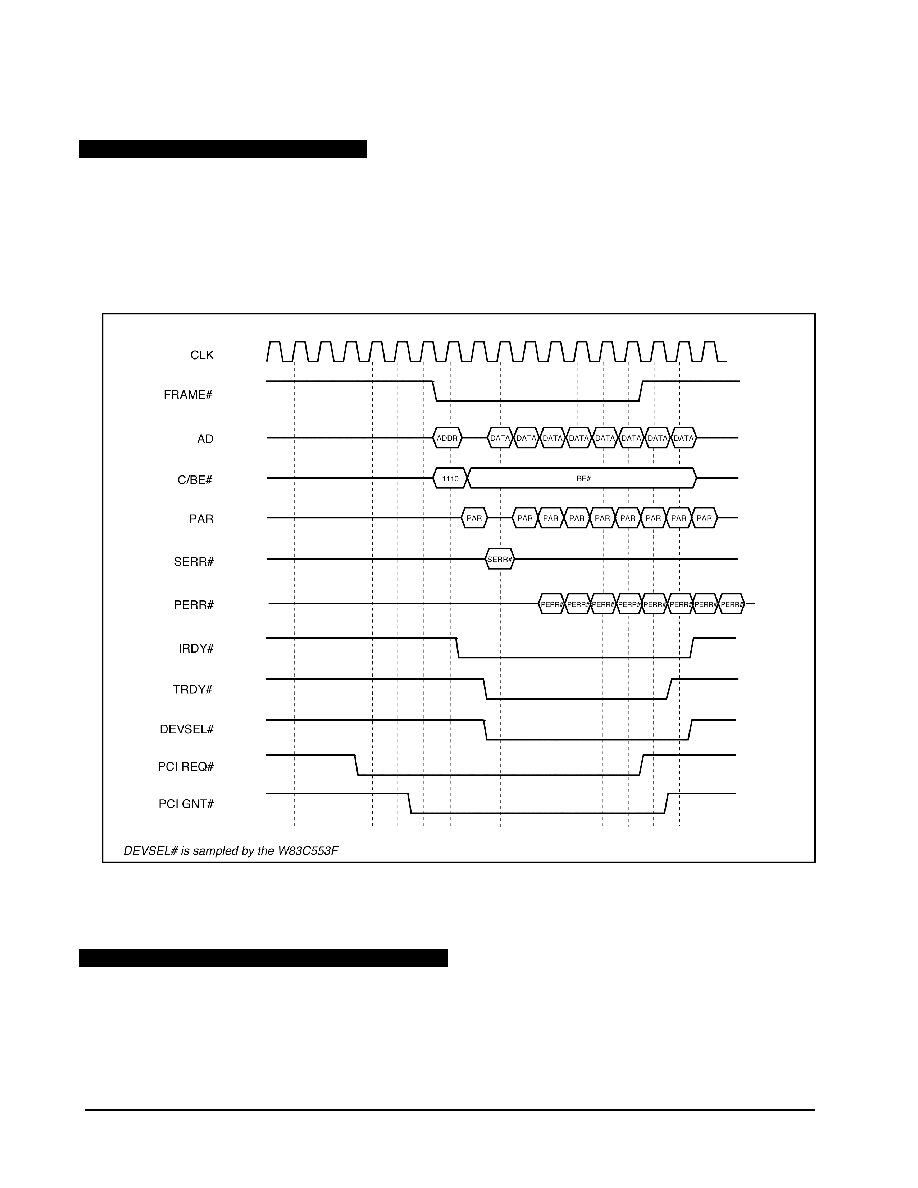
The Memory Read command (C/BE[3:0]# = 6h during the address phase) is only used when operating as a bus master. It
will be used when transferring data to memory and the number of data phases is one half or less of the value programmed to
the Cache Line Size Register, or when reading less than 2 Dwords from memory. If the device needs to read more than 2
Dwords from memory, the Memory Read Line command is used. During the Memory Read cycle, the W83C553F issues a
PCI REQ# for the bus and, when PCI GNT# is asserted, reads one Dword from system memory. The bus is then released.
The data phase in Figure 3-6 takes two clock cycles, as determined by TRDY#. The W83C553F activates all byte enables,
even if some byte lanes do not contain valid data. It internally discards unnecessary bytes.
In slave mode, PCI-to-ISA memory reads are supported.
Figure 3-6. Master Memory Read Timing
W83C553F Electrical Specifications
WINBOND SYSTEMS LABORATORY
39
3.11 PCI Memory Write
The Master Memory Write command (C/BE[3:0]# = 7h during the address phase) cycle is used by the W83C553F when
writing to memory. The W83C553F issues a request for the bus and, when granted access, writes one Dword to system
memory. The bus is then released. The data phase in Figure 3-7 takes two clock cycles, as determined by TRDY#.
In slave mode, PCI-to-ISA memory writes and ROM writes are supported.
Figure 3-7. Master Memory Write Timing
W83C553F Electrical Specifications
WINBOND SYSTEMS LABORATORY
40
3.12 PCI Memory Read Line
The Memory Read Line command (C/BE[3:0]# = Eh during the address phase) is only used when operating as a bus master.
It will be used when transferring data to memory and the number of data phases is at least two double words and is greater
than one half of the value programmed to the Cache Line Size Register.
In Figure 3-8, the W83C553F issues a request for the bus and, when access is granted, reads eight Dwords from system
memory before releasing the bus. All data phases in this figure take one clock cycle, as determined by TRDY#.
Figure 3-8. Master Memory Read Line Timing
3.13 PCI Memory Write and Invalidate
The Memory Write and Invalidate command (C/BE[3:0]# = Fh during the address phase) is only used when operating as a
bus master and enabled as indicated by the state of the MWIEN bit of the Device Control Register. It will be used when
transferring data from memory and entire cache line(s) will be written (as programmed to the Cache Line Size Register).
W83C553F Electrical Specifications
WINBOND SYSTEMS LABORATORY
41
3.14 Transaction Termination
The termination of a PCI transaction can be initiated by either the master or target. During termination, the master controls
the completion of all PCI transactions, regardless of what caused the termination. All transactions are concluded when
FRAME# and IRDY# are de-asserted, indicating an IDLE cycle.
When the W83C553F is a bus master, its PCI bus cycles may be terminated by the target as a Disconnect With Data Transfer,
Disconnect Without Data Transfer, or Target Abort. The W83C553F's PCI bus cycles may also be terminated by the
W83C553F itself as a Preemption or a Master Abort.
3.14.1 PCI Disconnect With Data Transfer Timing
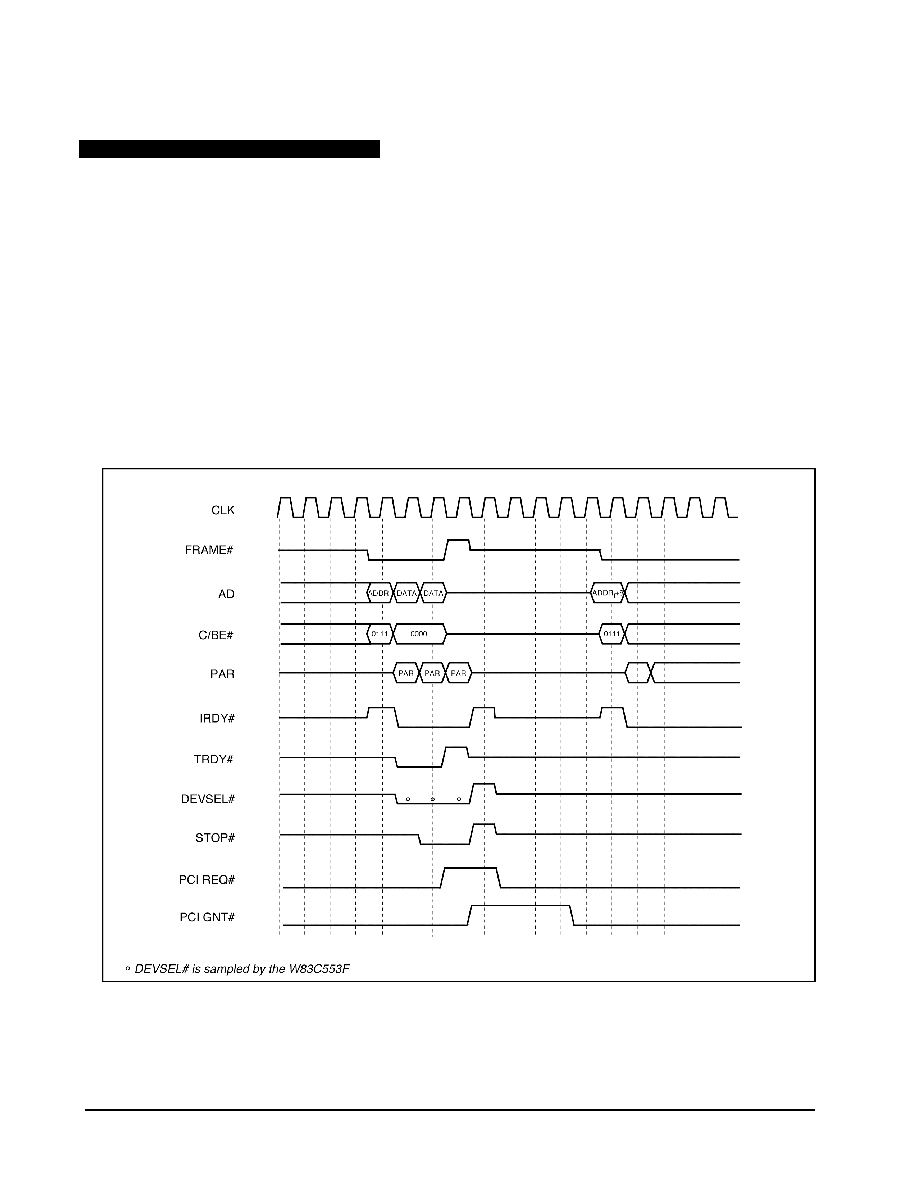
The Disconnect With Data Transfer command cycle of Figure 3-9 shows one last data transfer occurring after the target
asserts STOP# to start the termination sequence. The data is still transferred, since IRDY# and TRDY# are asserted. The
W83C553F terminates the current transfer with de-assertion of FRAME#, and the de-assertion of IRDY#, at which point it
releases the bus. The W83C553F will re-request the bus after two clock cycles if more data is to be transferred. The starting
address of the new transfer will be the address of the next untransferred data.
Figure 3-9. Disconnect With Data Transfer Timing
W83C553F Electrical Specifications
WINBOND SYSTEMS LABORATORY
42
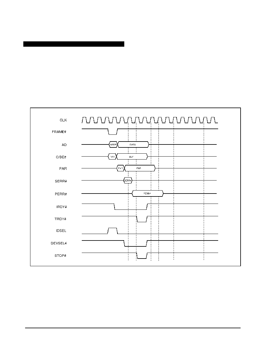
3.14.2 PCI Disconnect Without Data Transfer Timing
The Disconnect Without Data Transfer command cycle of Figure 3-10 shows a target disconnect when no data is transferred.
STOP# is asserted without TRDY# being asserted at the same time. The W83C553F terminates the current transfer with de-
assertion of FRAME#, and the de-assertion of IRDY#, at which point it releases the bus. The W83C553F will re-request the
bus after two clock cycles if more data is to be transferred. The starting address of the new transfer will be the address of the
next untransferred data (i.e. the address that the data would have been transferred to had the disconnect not occurred).
Figure 3-10. Disconnect Without Data Transfer Timing
W83C553F Electrical Specifications
WINBOND SYSTEMS LABORATORY
43
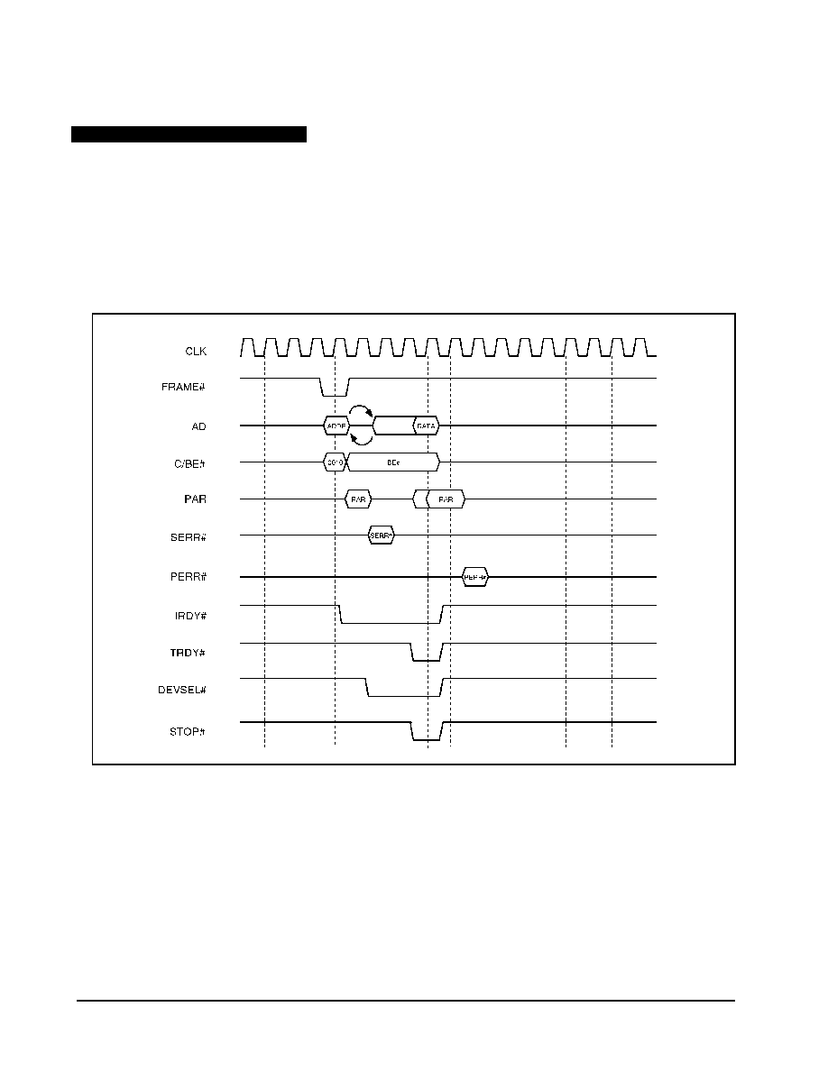
3.14.3 PCI Target Abort Timing
The Target Abort cycle of Figure 3-11 starts when the target asserts DEVSEL# for one clock, then de-asserts DEVSEL# and
asserts STOP#. A target can use this sequence to indicate it cannot service the data transfer, and does not want the
transaction retried. The W83C553F cannot assume any data transfers in the current transaction were successful. It
terminates the current transfer with the de-assertion of FRAME#, and IRDY#. Since data integrity is not guaranteed, the
W83C553F cannot recover from a target abort event. Any on-going IDE activity will be stopped immediately, and an
interrupt will be generated if enabled. Abort and Error bits in the DMA Status register will be set. The PCI Configuration
registers will not be cleared. The PCI Configuration Space Status Register's RTA bit will be set to indicate the W83C553F
has received a Target Abort.
Figure 3-11. Target Abort Timing
W83C553F Electrical Specifications
WINBOND SYSTEMS LABORATORY
44
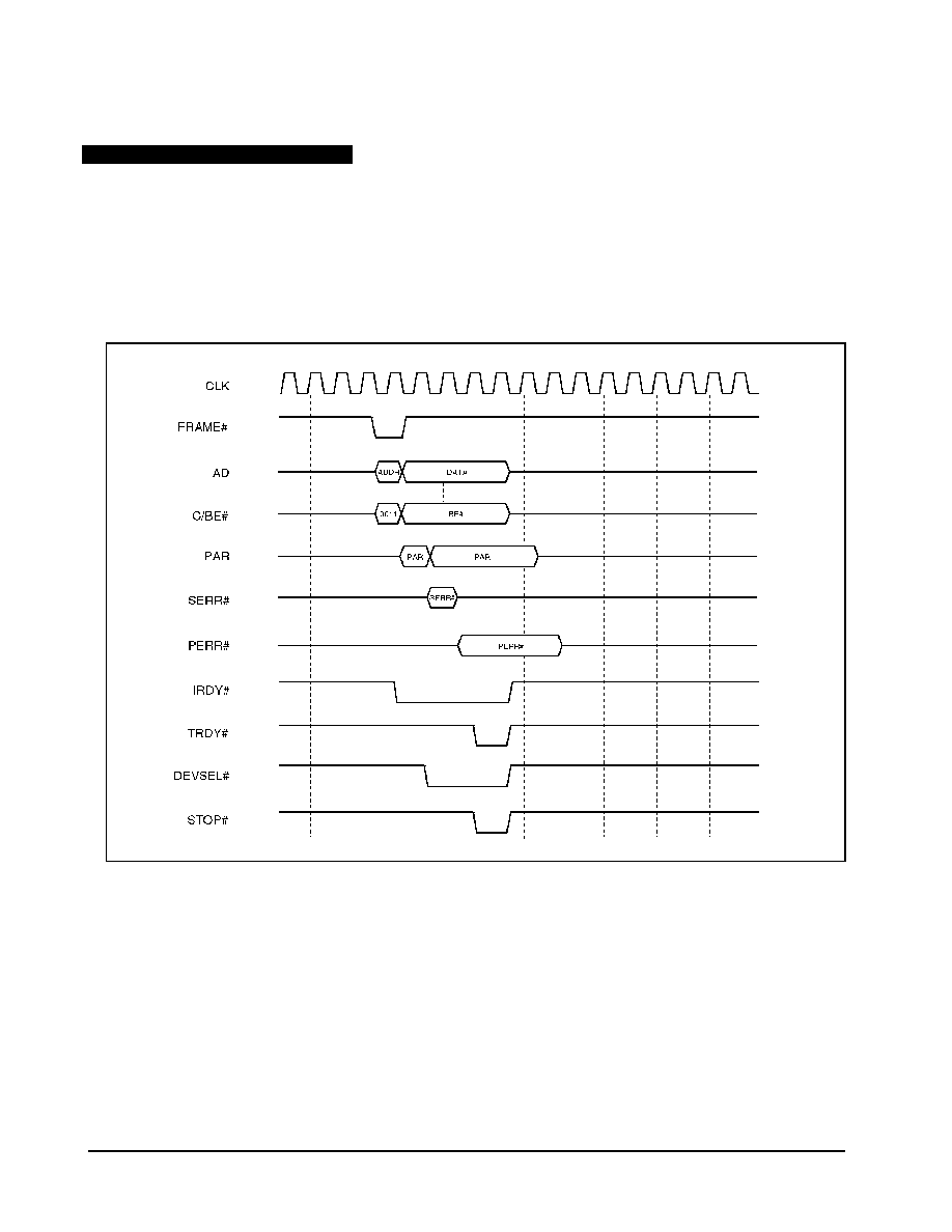
3.14.4 PCI Preemption Timing
The main arbiter can void the PCI GNT# signal sent to the W83C553F, if the current bus cycle takes too long, as in the case
of DMA bursts. When PCI GNT# is removed, and the value in the Latency Timer Register has reached zero, the W83C553F
will finish the current transfer, and immediately release the bus. The timer in the W83C553F PCI configuration space is
programmable. The W83C553F will keep PCI REQ# asserted to regain bus ownership.
Figure 3-12. Preemption Timing

W83C553F Electrical Specifications
WINBOND SYSTEMS LABORATORY
45
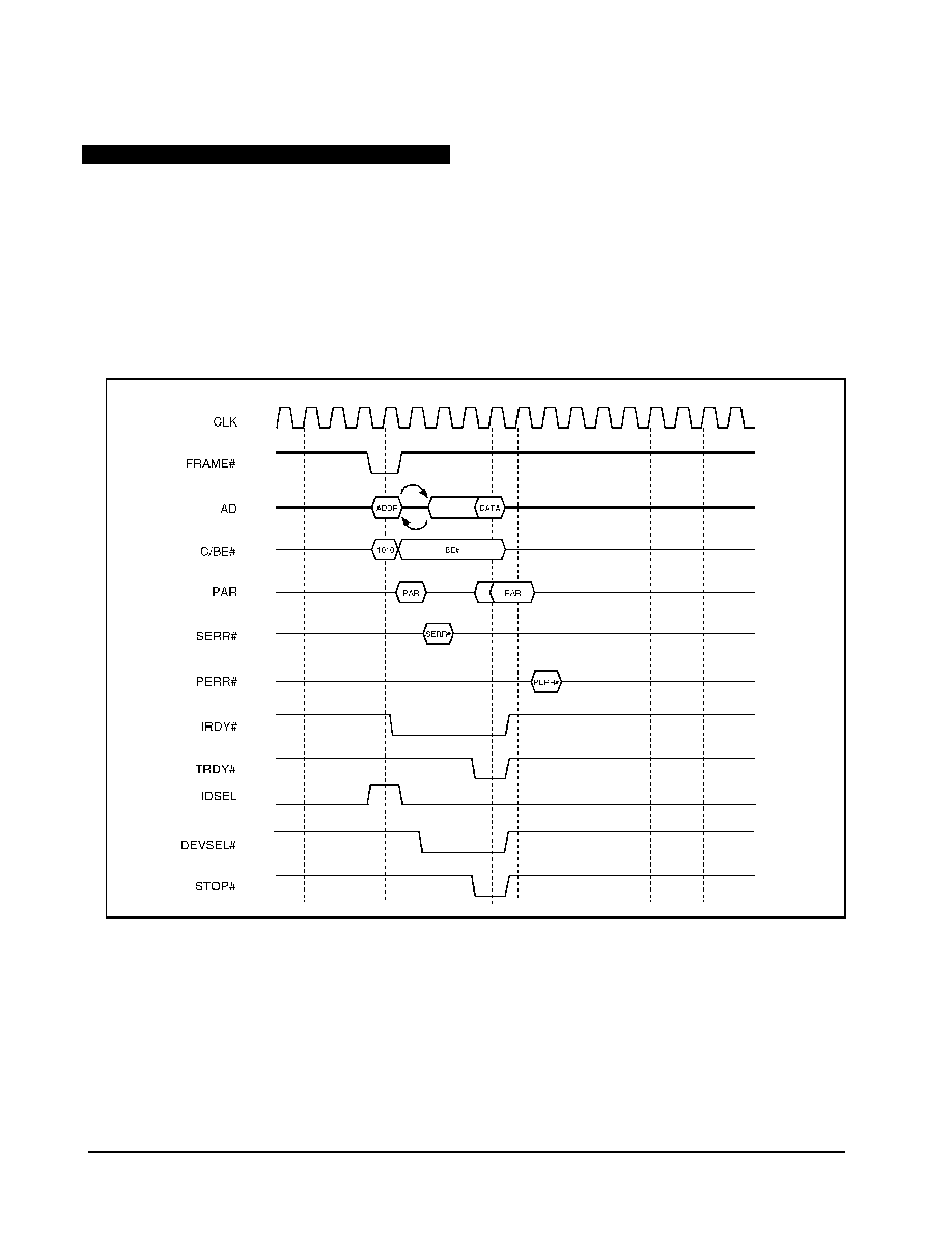
3.14.5 PCI Master Abort Timing
A Master Abort sequence is initiated by the W83C553F to abort its cycle if DEVSEL# is not asserted within four clocks after
FRAME# is asserted. This sequence is treated as a fatal error. Any IDE activity will be terminated immediately. An NMI
will be generated if programmed in register 40h, bit 0 (page 58.) The DMA Status Register's Abort and Error bits will be set.
The PCI Configuration Registers will not be cleared. The PCI Configuration Space Status Register's MA bit will also be set,
to indicate the W83C553F has terminated its transaction using a Master Abort cycle.
Figure 3-13. Master Abort Timing

W83C553F Electrical Specifications
WINBOND SYSTEMS LABORATORY
46
3.15 IDE Interface Operation
Operation of the IDE interface is controlled by the configuration registers. Port 0 (Primary Port) and Port 1 (Secondary Port)
have the same features, capabilities and configuration options. All 8-bit timing is fixed. The following table shows the 8-bit
fixed timing.
Although the 16-bit timing (host cycle 16/32-bit) is programmable on a cycle basis (on/off time), most of the 16-bit cycle
timing is also fixed. Address setup, address hold, and data hold (write) times will be the same as for the 8-bit cycles. Data
setup time will be equal to the write command on time. This allows the user to only program the command on/off times to
select PIO Mode 0, 1, 2, 3, 4 or 5 (proposed), and DMA Single and Multiword 0, 1 or 2 timing.
Much of the DMA mode timing is also fixed. When DMA transfers are executed on the IDE interface, the selected ports'
chip selects (IDECS0# and IDECS1# for primary and secondary) will be de-asserted (high) when the BMEN bit in the
associated Bus Master Control Register is set to "1." When the IDE device asserts IDEDRQ[A:B], the W83C553F will
immediately assert IDEDAK[A:B]# if BMEN is set. One clock later the IDEIOW[A:B]# or IDEIOR[A:B]# output will be
asserted. For multiword DMA transfers, the IDEIOW[A:B]# or IDEIOR[A:B]# signal will free run at the programmed rate
as long as DRQ remains asserted and the W83C553F is prepared to complete a data transfer. If IDEDRQ[A:B] has not de-
asserted by the rising edge of the IDEIOW[A:B]# or IDEIOR[A:B]# signal multiword DMA is assumed and at least one
more cycle will be executed. If DRQ de-asserts at any time after IDEDAK[A:B]# is asserted but before IDEIOW[A:B]# or
IDEIOR[A:B]# is de-asserted, this will be the last cycle until DRQ re-asserts. In this case, IDEDAK[A:B]# will be de-
asserted one clock after the IDEIOW[A:B]# or IDEIOR[A:B]# signal de-asserts. This allows for the support of the single
and multiword DMA cycles automatically.
Table 3-3 Eight-bit Fixed Timing
Parameter
Time (CLKs)
SPD ="1"
Command on
10
Command off
10
Address setup
3
Address hold
1
Data setup (wr)
3
Data Hold (wr)
1
Cycle time
20
If CLK < 33 MHz, then the timing in Table 3-3 is ATA Mode 0 compatible.

W83C553F Electrical Specifications
WINBOND SYSTEMS LABORATORY
47
3.16 PIO Transfers
When transferring data with the PIO protocol, I/O read/write cycles are executed on the IDE interface and PIO transfers are
executed on the PCI bus. The IDE interface address and chip select signals will only change when a decoded cycle is
detected on the PCI bus. This minimizes IDE interface switching and EMI noise. Once a 16 or 32 bit cycle to a data port is
detected, the W83C553F will setup the proper address and chip selects. Once the address setup time has been met,
IDEIOR[A:B]# or IDEIOW[A:B]# will be asserted and held on until the on command time has been met. The W83C553F
will then de-assert IDEIOR[A:B]# or IDEIOW[A:B]# and hold the addresses and chip selects stable. If read ahead or posted
writes are enabled for this device, read or write cycles will be executed at the programmed on/off timing until the read ahead
buffer is full, the read ahead count is complete, or the posted write buffer is empty. This will maximize the IDE interface
performance because the address setup and hold timing will only add overhead at the beginning and end of a block transfer.
All timing in between is controlled by the command on/off times or the host throughput which ever is slower. The
IDEIOR[A:B]# / IDEIOW[A:B]# signals will never be asserted (cycle committed) if the FIFO is full/empty.
If an 8 bit cycle to a different register is decoded on the PCI bus while read ahead is active, the read ahead buffer will be
preserved, the read ahead will pause and the 8 bit cycle will be executed. Once the 8 bit cycle is completed the read ahead
will resume if a 16 or 32 bit data port read is decoded on the PCI bus. This allows for the host to check the status register
during a data transfer without loosing data.
If an 8 bit cycle to a different register is decoded on the PCI bus while posted write is active, the posted write buffer will be
written to the IDE device while inserting wait states to the PCI bus. Once the write buffer is empty, the 8 bit cycle will be
executed.
The IDE interface and buffers will not be affected by the W83C553F configuration cycle accesses.
During data port read cycles with read ahead active, if an interrupt is detected on the IDE interface it will not be passed to the
PCI bus until the data buffer is empty.
The 16-byte PIO FIFO allows the two channels to transfer data simultaneously without corrupting data between the channels.
Past dual port chips required that interrupts be disabled during a data transfer because only one data FIFO existed and being
interrupted out of a transfer to access the second port caused the read ahead/posted write data in the FIFO to be lost or
corrupted.
All accesses to configuration registers and all 8 bit IDE accesses will be executed in the real time (read ahead and posted
write not used). Only 16 and 32 bit cycles to an IDE data register will support read ahead or posted writes.
W83C553F Electrical Specifications
WINBOND SYSTEMS LABORATORY
48
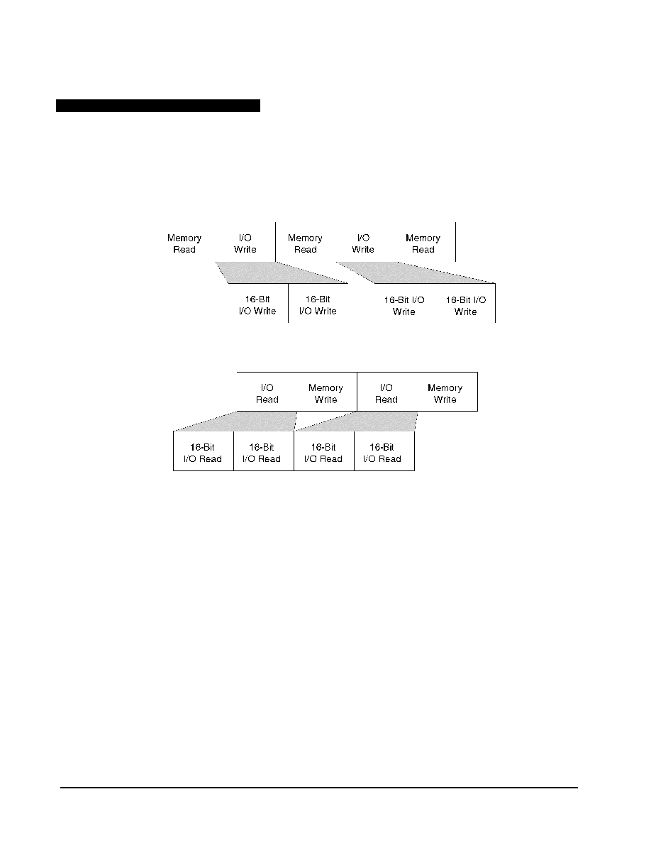
3.17 32-Bit Data Transfers
32-bit data transfers are used to reduce system overhead and improve performance. The standard PIO protocol requires the
system CPU to execute an I/O cycle and a memory cycle to move two bytes of data between the IDE device and memory. To
transfer 4 bytes of data would require two I/O cycles and two memory cycles. This can be accomplished with one 32-bit I/O
and one 32-bit memory cycle. This cuts the CPU cycles in half. By enabling read ahead, the IDE read cycles will be
buffered from the PCI bus and execute in parallel with the system memory reads cutting overhead more. Enabling posted
writes will similarly improve write performance.
PCI Bus 32-Bit PIO Write Cycle
IDE Write Cycle with Posted Writes
PCI Bus 32-Bit PIO Read Cycle
IDE Read Cycle with Read Ahead
The two drawings shown above show the relationship
between the PCI bus and the IDE interface.

W83C553F Electrical Specifications
WINBOND SYSTEMS LABORATORY
49
3.18 Bus Master Transfers
When operating as a bus master on the PCI bus, DMA cycles will be executed on the IDE interface. In this mode, once the
BMEN bit of the Bus Master Control Register is set the W83C553F will de-assert the chip selects for that port and respond to
DRQ as defined above. If an interrupt is generated on the IDE interface, it will be delayed for IDE device to memory
transfers until the FIFO is empty (written to memory). The IDEIOW[A:B]#/IDEIOR[A:B]# will be held high and not
asserted (pause) any time that the FIFO is empty/full.
To maximize the PCI bus bandwidth, the bus master FIFO is independent of the PIO FIFOs. It is 64 bytes deep which allows
the W83C553F to burst transfers of 8 double words consistently. This allows the use of the Memory Read Line and Memory
Write And Invalidate commands.
If both ports operate in the bus master mode, they will share the same FIFO and a fairness arbitration will be employed to
guarantee both ports have transfer time slices.
Using this protocol to transfer data relieves the System CPU overhead by 90% typically. This is achieved because the CPU
only needs to send the command to the target IDE device, set up the bus master PRD table, and program the bus master
register set. There will only be one interrupt per command to service, whereas PIO commands require one interrupt per
sector or block of sectors, and the CPU must manually transfer all data.
PCI bus utilization is also reduced by up to 90% over the standard PIO protocol. The bus master core can transfer one sector
of data with less than 6 microseconds of active bus time, regardless of the IDE device transfer rate. The same PIO transfer
requires over 150 microseconds of active bus time, when using a Mode 0 IDE device.
3.19 82C59A Interrupt Controller
Two interrupt controllers are included in the W83C553F, and are internally cascaded to handle a total of 15 interrupt
channels. IRQ0 is internally connected to OUT0, of the 82C54 counter/timer. Typically, an interrupt is generated by the
rising edge of an IRQ signal. However, IRQ8 and IRQ13 are fixed to trigger on the falling edge, allowing direct connection
to the real time clock interrupt (IRQ8#), or Pentium CPU floating point error signal (FERR#). Also, RX 4D0h and RX 4D1h
can be programmed to change the IRQs from edge sensitive to level sensitive interrupts. All external IRQ lines are internally
pulled-up to eliminate noises on unconnected request pins. I/O port and channel definition matches that of the IBM PC/AT
requirement.
3.20 82C37A DMA Controller
Two 82C37A DMA controllers are integrated into the W83C553F. Each controller is a four channel DMA device,
generating memory addresses and control signals necessary to transfer information between a peripheral device and memory,
without CPU intervention.
The two controllers are cascaded to provide four DMA channels permitting 8-bit peripheral device data transfers. Three
channels permit 16-bit peripheral device data transfers. The I/O port and channel definition matches that of the IBM PC/AT
requirement.
Type A, B and F DMA are supported in the W83C553F. Both DMA controllers support full 32-bit addressing and
scatter/gather transfer capability.

W83C553F Electrical Specifications
WINBOND SYSTEMS LABORATORY
50
3.21 82C54 Counter/Timer
One 82C54 counter/timer, with three channels, is included in the W83C553F. The clocks for the three channels are
connected to the 14.31818 MHz clock through a divide-by-twelve counter. The gate inputs of counters 0 and 1 are tied high
so that they are always enabled. The gate input of counter 2 is tied to bit 0 of Port B, inside the chip. The output of counter 0
is connected to the IRQ0 input of the interrupt controllers. The output of counter 1 goes to the arbitration logic for a refresh
request. Finally, the output of counter 2 goes to an AND gate, which drives the SPKR output pin. The other input to this
AND gate comes from bit 1 of Port B.
3.22 PCI Arbiter
The W83C553F contains a programmable, eight master PCI arbiter which can be tailored to meet system-specific arbitration
requirements. Pin 16 is available to strap the arbiter into its disabled state on power-up. A weak 2.2K ohm pull-down
resistor is recommended for this in systems using an external arbiter. When disabled, the "Function 0" ISA bridge uses the
REQ#/GNT# pair on pins 25 and 26, and the "Function 1" IDE uses the REQ#/GNT# pair on pins 27 and 28. If no pull-
down resistor is used on pin 16, the on-chip arbiter will "come up" enabled after power up.
When in the active state, the eight masters supported by the W83C553F are its two internal masters (ISA bridge and IDE),
the system CPU, and REQ#/GNT#[4:0] which are available to the system designer. The PCI5TH# function of pin 13 can be
used to change the fifth REQ#/GNT# pair (on pins 6 and 7) to FLSHREQ#/FLSHACK# if desired (in either CPU mode).
This PCI5TH# function is automatically overidden by the ARBDIS# pin when enabled.
FLSHREQ#/FLSHACK# are only used in Guaranteed Access Timing (GAT) mode. In GAT mode, before Function 0 makes
a request for the PCI bus, it asserts FLSHREQ# to the system and waits for FLSHACK# to be asserted. The system can use
this signal to flush all PCI buffers so that the W83C553F can be granted unimpeded access to main memory. When Function
0 (PCI-to-ISA bridge) is not in GAT mode, it behaves as any other PCI master device.
Upon power-up, the arbiter defaults to a "round-robin" rotation scheme allowing all PCI masters equal access to the local bus.
If desired, the relative priority of each REQ/GNT pair can be custom tailored to a specific system design via the PCI Priority
Control Register 1 at Index 80h in the Function 0 PCI Configuration Space. Note that all masters are assured of access to the
PCI bus at least once during each rotation regardless of the programming options chosen. (This is required for PCI
compliance, so no functions are "locked out" for an extended period).

W83C553F Electrical Specifications
WINBOND SYSTEMS LABORATORY
51
3.23 Break Events
Break events include IRQ0 - IRQ15, DRQ0 - DRQ7, SERR#, ISA IOCHK#, INTR and non-maskable interrupts to the CPU
(NMI). OEM designers can program Function 0 PCI Configuration Registers 60h - 63h to select individual IRQs and DRQs
as the break events. These registers allow the W83C553F to function within a comprehensive power management scheme
with an external power management unit (as located on CPU-to-PCI bridge devices) in a green PC application.
3.24 CPU Modes (X86 or PowerPC)
The W83C553F incorporates two different CPU modes which change the functionality of several pins on the chip. An x86
mode supports any Intel-compatible microprocessor, including Pentium, AMD K5, Cyrix M1, NexGen 586, Intel P6, and
others. A PowerPC mode supports the IBM/Apple/Motorola PowerPC microprocessor Common Hardware Reference
Platform, as well as other RISC CPUs, such as DEC Alpha, Sun SPARC, and MIPS R4xxx CPUs.
Following is a summary of pins which change functionality depending on which CPU mode is chosen for the W83C553F via
strapping pin 8 high (PowerPC) or low (x86) with a weak (2.2K ohm) resistor:
Pin # x86 Function PowerPC Function
4 IGNNE# HRESET#
5 PMACT# ISARST
22 A20M# PCIRST#
116 XRD# SECURITY/XRD#
118 XCS1 X8XCS
119 XCS0 ROMCS
It can be seen from the above table (and the respective pin descriptions on pages 12-25) that the W83C553F is able to
generate all of the required reset signals for the microprocessor, PCI bus, and ISA bus when in PowerPC (non-x86) mode.

W83C553F Electrical Specifications
WINBOND SYSTEMS LABORATORY
52
4.0 REGISTER INFORMATION
The W83C553F SIO controller with PCI arbiter is a multi-function PCI device. Function 0 is the ISA bridge, and Function 1
is the bus master IDE controller. The registers summarized in this section are organized as follows:
� PCI Configuration Space - ISA Bridge Registers (Function 0)
� ISA Bridge (Function 0) I/O Registers
� PCI Configuration Space - Bus Master IDE Registers (Function 1)
� Bus Master IDE (Function 1) I/O Registers
Each function of the W83C553F SIO chip supports a complete set of configuration registers as defined in the PCI Spec. Rev.
2.1 for a 32-bit bus implementation. Additional configuration registers are supported for bus master and IDE port/device
control. They can be accessed whenever the PCIRST# signal is de-asserted. These registers are internal to the W83C553F,
and control the operation of the chip when responding to bus I/O cycles.
They are accessed when a configuration bus cycle is executed with IDSEL asserted and AD[1:0] both low. All registers are
implemented as 32-bit registers and the C/BE[3:0]# inputs determine which byte lanes are read/written. This allows the
registers to be accessed 8, 16, 24, or 32 bits at a time. The specific 32-bit register is directly addressed by AD[7:2].
All reserved bits and bytes return a logic 0 when read. All reserved bytes written will execute normal PCI cycles, but will not
affect the operation or device registers.
The internal register information for the W83C553F is organized as follows:
� Register name and Index value offset from base address.
� Type (Read and/or Write).
� Bit description.

W83C553F Electrical Specifications
WINBOND SYSTEMS LABORATORY
53
W83C553F Register Accessibility
Functional Block
Address Range (Hex)
ISA
PCI
Broadcasted
Config. Space
0-FF
X P
PIC 1
20-21
X P X P
Counter/Timer
40-43
X P X P
Port B
61
X P X P
RTC Index (shadow)
70 write
X P X P
X P
DMA Page
81, 82, 83, 87, 89, 8A, 8B
X P X P
Port 92
92
X P X P
X P
PIC2
A0-A1
X P X P
Co-processor Error
F0 write
X
X
X
DMA1
0-F
X P
BMTR
78-7B
X P
DMA2
C0-DE
X P
Interrupt Mode
4D0-4D1
X P
RTC CMOS RAM
810, 812
P
P
X = accessible in x86 mode
P = accessible in PowerPC mode
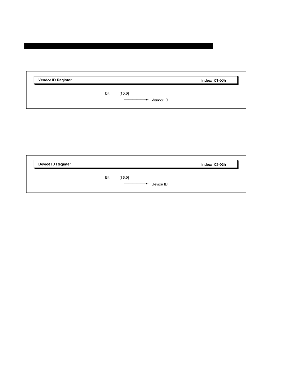
W83C553F Electrical Specifications
WINBOND SYSTEMS LABORATORY
54
4.1 PCI Configuration Space - ISA Bridge Registers (Function 0)
4.1.1 Function 0 Header Registers
Vendor ID Register (default = 10ADh)
Bit Description:
Bits [15:0]: VENDID. Vendor ID for Symphony Laboratories is 10ADh.
Device ID Register (default = 0565h)
Bit Description:
Bits [15:0]: DEVID. Device ID for ISA bridge is 0565h.

W83C553F Electrical Specifications
WINBOND SYSTEMS LABORATORY
55
Command Register (default = 0007h)
Type: Read/Write
Bit Description:
Bits [15:10]: Reserved. These read only bits are all set to "0".
Bit 9: Fast Back-to-Back Enable. W83C553F does not generate fast back-to-back cycles. This read
only bit is set to "0".
Bit 8: SERR# Enable. W83C553F does not drive the SERR# pin. Defaults to "0".
Bit 7: Wait Cycle Control. W83C553F does not use address/data stepping. This read only bit is set
to "0".
Bit 6: Parity Error Response. This is a read/write bit.
Bit 5: VGA Palette Snoop. W83C553F is not a VGA device. This read only bit is set to "0".
Bit 4: Memory Write and Invalidate Enable. W83C553F does not generate memory write and
invalidate commands. This read only bit is set to "0".
Bit 3: Special Cycles. W83C553F ignores all special cycles when reset. Defaults to "0".
Bit 2: Bus Master. Always enabled. This read only bit is set to "1".
Bit 1: Memory Space. Always enabled. This read only bit is set to "1".
Bit 0: I/O Space. Always enabled. This read only bit is set to "1".
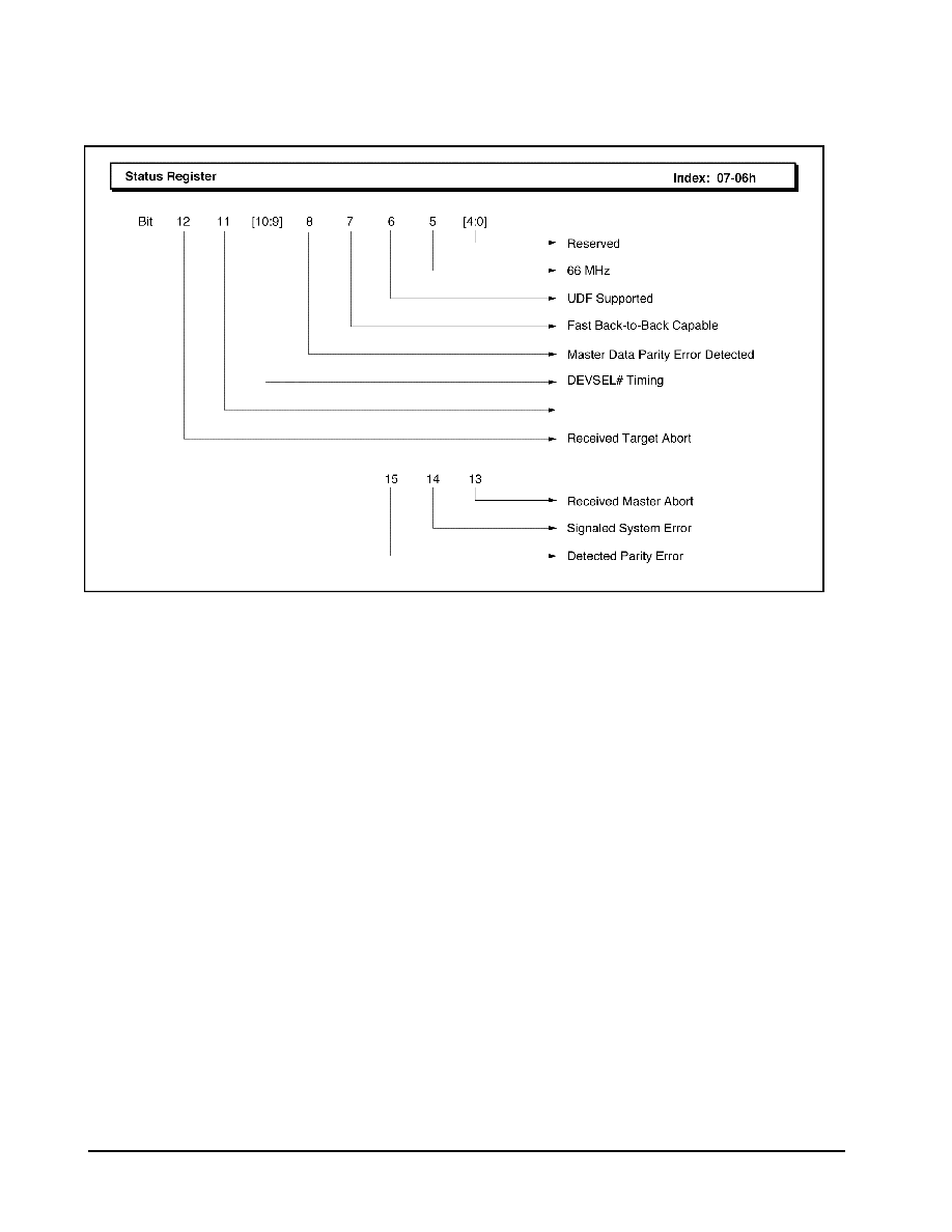
W83C553F Electrical Specifications
WINBOND SYSTEMS LABORATORY
56
Status Register (default = 0200h)
Type: Read/Write
Bit Description:
Bit 15: Detected Parity Error (DPE). This bit is read/write.
Bit 14: Signaled System Error (SSE).
Bit 13: Received Master Abort (RMA). This bit is read/write.
Bit 12: Received Target Abort (RTA). This bit is read/write.
Bit 11: Signaled Target Abort (STA). This bit is read/write.
Bits [10:9]: DEVSEL# Timing (DVSLT). Medium speed. These read only bits are both set to "01".
Bit 8: Master Data Parity Error Detected (MDPE). This bit is read/write.
Bit 7: Fast Back-to-Back Capable (FB2BC). W83C553F does not decode fast back-to-back cycles
across different targets. This read only bit is set to "0".
Bit 6: UDF Supported (UDFS). W83C553F does not support user definable features. This read only
bit is set to "0".
Bit 5: 66 MHz Capable (PCI66C). W83C553F does not support 66 MHz bus speed. This read only
bit is set to "0".
Bits [4:0]: Reserved. This read only bit is set to "0".
Signaled Target Abort

W83C553F Electrical Specifications
WINBOND SYSTEMS LABORATORY
57
Revision ID Register (default = 00h)
Bit Description:
Bits [7:0]: REVID. Revision ID for ISA Bridge is 00h.
Class Code Register (default = 060100h)
Bit Description:
Bits [23:16]: BCLASS. Base Class is 06h. Bridge device.
Bits [15:8]: SCLASS. Sub-Class is 01h. ISA bus.
Bits [7:0]: PROGIF. Programming Interface is 00h.
Header Type Register (default = 80h)
Bit Description:
Bit 7: MFCN. Multi-Function Device is "1". W83C553F contains two functions (ISA bridge and IDE
master).
Bits [6:0]: CFGLAY. Configuration Layout is 00h. Non-PCI-to-PCI bridge device.
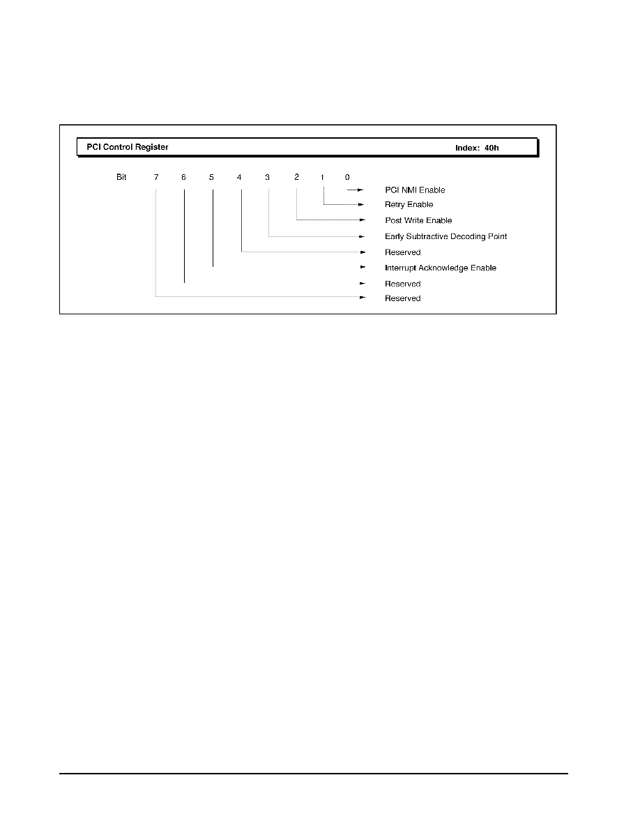
W83C553F Electrical Specifications
WINBOND SYSTEMS LABORATORY
58
4.1.2 Function 0 Control Registers
PCI Control Register (default = 20h)
Type: Read/Write
Bit Description:
Bit 7: Reserved. This read only bit is set to "0".
Bit 6: Reserved.
Bit 5: IAE. Interrupt Acknowledge Enable. Setting this bit allows the W83C553F chip to respond to
the interrupt acknowledge command. This bit is active after reset.
Bit 4: Reserved. This read only bit is set to "0".
Bit 3: ESDP. Early Subtractive Decoding Point. Setting this bit will move the subtractive decoding
point one PCI clock earlier from "slow" to "medium" timing.
Bit 2: PWE. Post Write Enable. Setting this bit will allow PCI memory write cycles to the ISA bus to
be posted.
Bit 1: RETRYE. Retry Enable. When this bit is set to "1", PCI slave cycles are retried when the
internal bus is busy. When this bit is reset to "0" and the internal bus is busy, a PCI slave cycle
will be held in wait states until the bus becomes idle and the access completes. The default
state of this bit after a hardware reset is "0".
Bit 0: PCI NMI Enable. When set, PCI error status bits in the Status Register (except SSE) will
generate an NMI. Defaults to "0".

W83C553F Electrical Specifications
WINBOND SYSTEMS LABORATORY
59
Scatter/Gather Relocation Base Address Register (default = 04h)
Function: The value programmed into this register determines the high order I/O adress of the Scatter/Gather
Command Registers, Scatter/Gather Status Registers, and Scatter/Gather Descriptor Table Registers.
The first Scatter/Gather register default address is at 0410h.
Type: Read/Write
Bit Description:
Bits [7:0]: AD[15:8]. These are the address bits of the relocated address space.
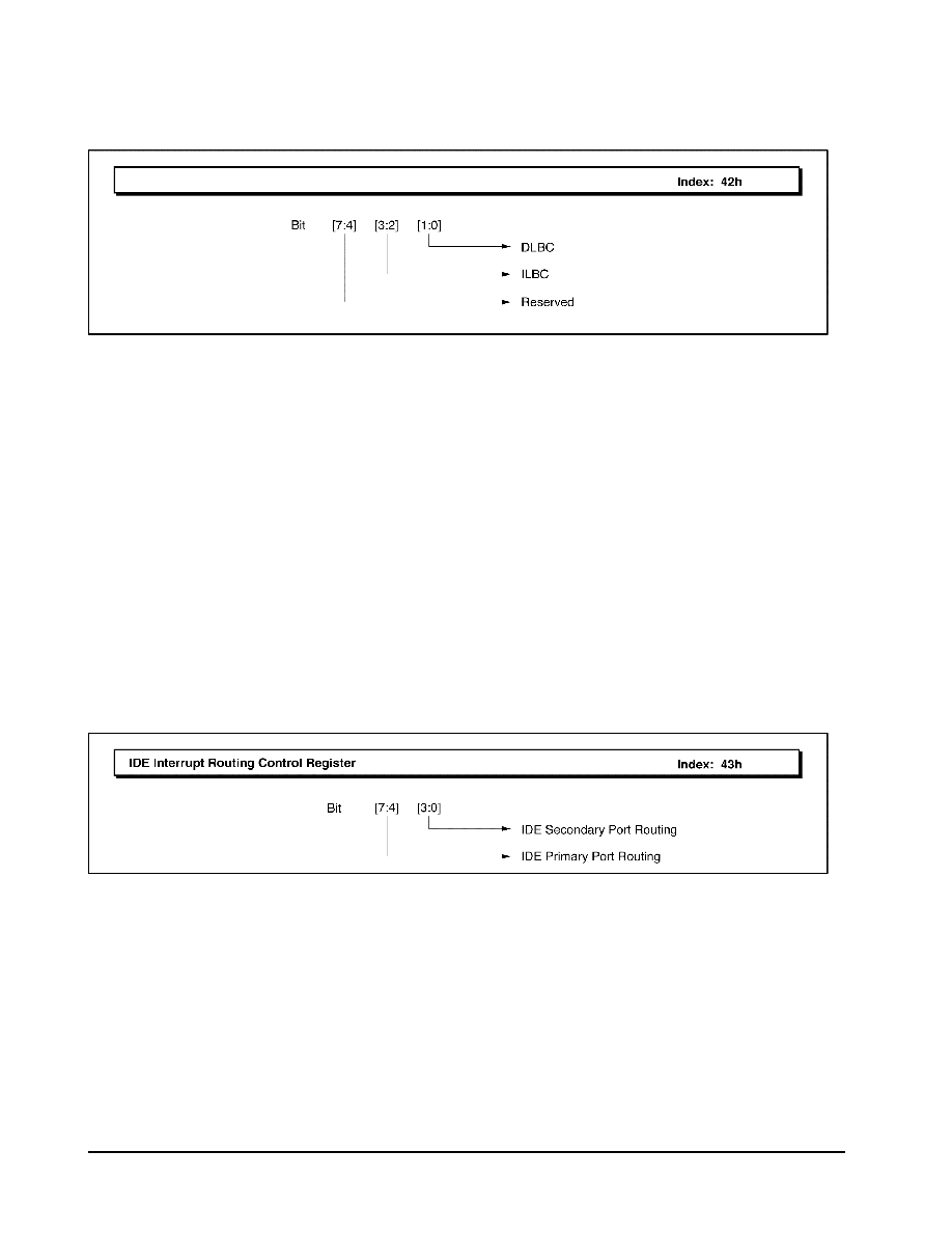
W83C553F Electrical Specifications
WINBOND SYSTEMS LABORATORY
60
Line Buffer Control Register (default = 00h)
Type: Read/Write
Bit Description:
Bits [7:4]: Reserved.
Bits [3:2]: ISA Master Line Buffer Configuration.
Bit 3 2 Function
0 0 Single transaction
0 1 Reserved
1 0 Reserved
1 1 Reserved
Bits [1:0]: DLBC. DMA Line Buffer Configuration.
Bit 1 0 Function
0 0 Single transaction
0 1 Reserved
1 0 Reserved
1 1 Reserved
IDE Interrupt Routing Control Register (default = EFh)
Type: Read/Write
Bit Description:
Bits [7:4]: IRQARCH [3:0]. Routes IDE Primary Port IRQ to the interrupt controller. Defaults to Eh
(IRQ14).
Bits [3:0]: IRQBRCH [3:0]. Routes IDE Secondary Port IRQ to the interrupt controller. Defaults to Fh
(IRQ15).
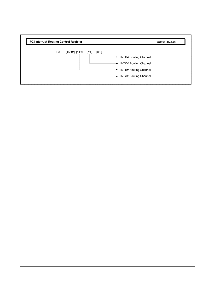
W83C553F Electrical Specifications
WINBOND SYSTEMS LABORATORY
61
PCI Interrupt Routing Control Register (default = 0000h)
Type: Read/Write
Bit Description:
Bits [15:12]: INTARCH [3:0]. INTA# Routing Channel. This field specifies the routing channel for INTA#.
Note channels 0, 1, 2, 8 and 13 are reserved. Setting this field to these values will disable
routing. Default value after a hardware reset is "0".
Bits [11:8]: INTBRCH [3:0]. INTB# Routing Channel. This field specifies the routing channel for INTB#.
Note that channels 0, 1, 2, 8 and 13 are reserved and setting this field to any of these values
will effectively disable routing. The default value after a hardware reset is "0".
Bits [7:4]: INTCRCH [3:0]. INTC# Routing Channel. This field specifies the routing channel for INTC#.
Note that channels 0, 1, 2, 8 and 13 are reserved and setting this field to any of these values
will effectively disable routing. The default value after a hardware reset is "0".
Bits [3:0]: INTDRCH [3:0]. INTD# Routing Channel. This field specifies the routing channel for INTD#.
Note that channels 0, 1, 2, 8 and 13 are reserved and setting this field to any of these values
will effectively disable routing. The default value after a hardware reset is "0".
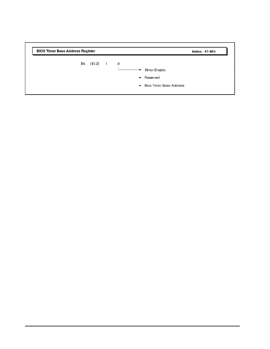
W83C553F Electrical Specifications
WINBOND SYSTEMS LABORATORY
62
BIOS Timer Base Address Register (default = 0078h)
Type: Read/Write
Function: The base address for the BIOS Timer Register located in PCI I/O space. The BIOS Timer resides in the
W83C553F and is the only internal resource mapped to PCI I/O space.
Bit Description:
Bits [15:2]: BTMRBA. BIOS Timer Base Address. This register specifies the Base Address 15:2 for the
BIOS Timer register located in the I/O space. The lower two bits of the base address are 00
(Dword aligned). The value of this register points to 78h (0000_0000_0111_10xx) after a reset.
Bit 1: Reserved.
Bit 0: BTMRE. Timer Enable. When this bit is set to "1", the BIOS timer function is enabled and the
base address of the timer registers is programmed in Bits [15:2].
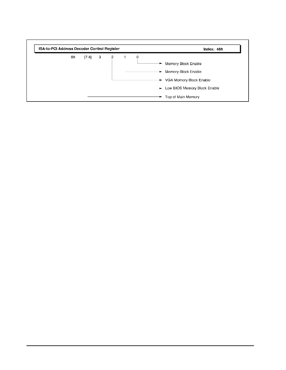
W83C553F Electrical Specifications
WINBOND SYSTEMS LABORATORY
63
ISA-to-PCI Address Decoder Control Register (default = 01h)
Type: Read/Write
Bit Description:
Bits [7:4]: IPATOM [3:0]. Top of Main Memory. Defines the top of memory for ISA memory space. ISA
memory accesses from 1 MByte to top of memory (except "hole") and above 16 MByte are
forwarded to the PCI bus.
Bit 7 Bit 6 Bit 5 Bit 4 Top of Memory
0 0 0 0 1 MByte
0 0 0 1 2 MByte
0 0 1 0 3 MByte
0 0 1 1 4 MByte
0 1 0 0 5 MByte
0 1 0 1 6 MByte
0 1 1 0 7 MByte
0 1 1 1 8 MByte
1 0 0 0 9 MByte
1 0 0 1 10 MByte
1 0 1 0 11 MByte
1 0 1 1 12 MByte
1 1 0 0 13 MByte
1 1 0 1 14 MByte
1 1 1 0 15 MByte
1 1 1 1 16 MByte
Bit 3: MBELBIOS. Low BIOS Memory Block Enable; 896-960 KByte (E0000-EFFFFh). When set to
"1", ISA memory accesses in this range are forwarded to the PCI bus. The LBIOSCSE bit
(UBCSA, configuration register 4Dh bit 6) overrides this bit.
Bit 2: MBEVGA. VGA Memory Block Enable; 640-768 KByte (A0000-BFFFF). When set to "1", ISA
memory accesses in this range are forwarded to the PCI bus.
Bit 1: MBE640. Memory Block Enable; 512-640 KByte (80000-9FFFFh). When set to "1", ISA
memory accesses in this range are forwarded to the PCI bus.
Bit 0: MBE512. Memory Block Enable; 0-512 KByte (0-7FFFFh). When set to "1", ISA memory
accesses in this range are forwarded to the PCI bus. This bit is set to "1" after reset.
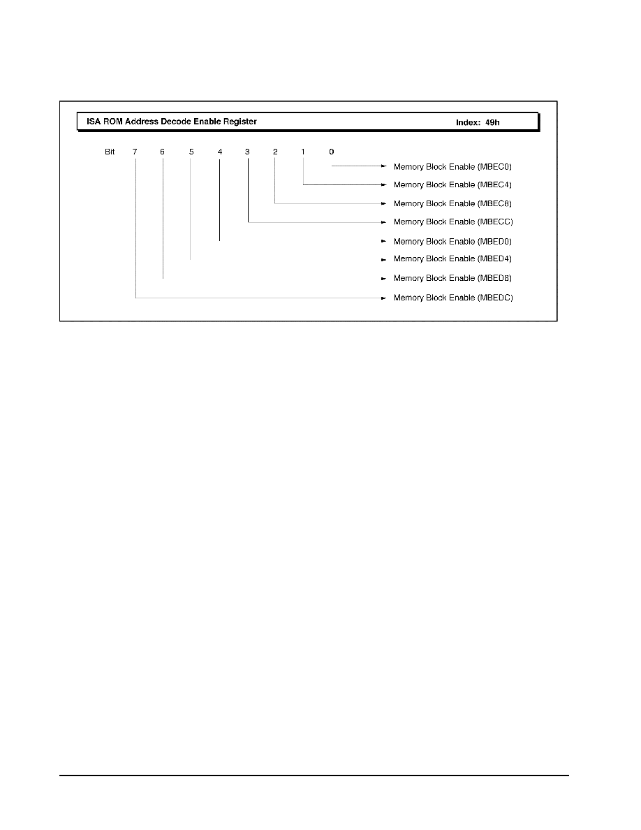
W83C553F Electrical Specifications
WINBOND SYSTEMS LABORATORY
64
ISA ROM Address Decode Enable Register (default = 00h)
Function: When a bit is set to "1", memory accesses to the corresponding address range in the add-on BIOS area
are forward to the PCI bus.
Type: Read/Write
Bit Description:
Bit 7: MBEDC. Memory Block Enable; 880-896 KByte. (DC000-DFFFFh).
Bit 6: MBED8. Memory Block Enable; 864-880 KByte. (D8000-CBFFFh).
Bit 5: MBED4. Memory Block Enable; 848-864 KByte. (D4000-C7FFFh).
Bit 4: MBED0. Memory Block Enable; 832-848 KByte. (D0000-C3FFFh).
Bit 3: MBECC. Memory Block Enable; 816-832 KByte. (CC000-CFFFFh).
Bit 2: MBEC8. Memory Block Enable; 800-816 KByte. (C8000-CBFFFh).
Bit 1: MBEC4. Memory Block Enable; 784-800 KByte. (C4000-C7FFFh).
Bit 0: MBEC0. Memory Block Enable; 768-784 KByte. (C0000-C3FFFh).
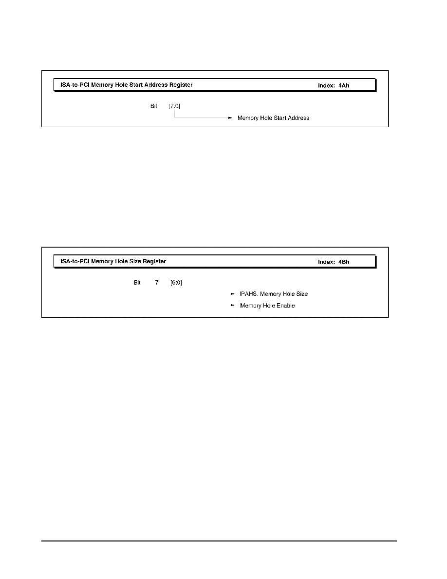
W83C553F Electrical Specifications
WINBOND SYSTEMS LABORATORY
65
ISA-to-PCI Memory Hole Start Address Register (default = 00h)
Type: Read/Write
Bit Description:
Bits [7:0]: IPAHA. Memory Hole Start Address. These 8 bits specify the 8 most significant bits of the ISA
address: LA[23:16].
Bit 7 Bit 6 Bit 5 Bit 4 Bit 3 Bit 2 Bit 1 Bit 0
LA23 LA22 LA21 LA20 LA19 LA18 LA17 SA16
ISA-to-PCI Memory Hole Size Register (default = 00h)
Type: Read/Write
Bit Description:
Bit 7: IPAHE. Memory Hole Enable. When this bit is set to "1", access to the memory hole will not be
forwarded to the PCI bus. When this bit is reset to "0", access to the hole will be forwarded to
the PCI bus. The default value of this bit after a chip reset is "0".
Bits [6:0]: IPAHS. Memory Hole Size. This field specifies the sizes of the memory hole according to the
following list:
Bit 6 Bit 5 Bit 4 Bit 3 Bit 2 Bit 1 Bit 0
0 0 0 0 0 0 0 = 64 KBytes
0 0 0 0 0 0 1 = 125 KBytes
0 0 0 0 0 1 1 = 256 KBytes
0 0 0 0 1 1 1 = 512 KBytes
0 0 0 1 1 1 1 = 1 MBytes
0 0 1 1 1 1 1 = 2 MBytes
0 1 1 1 1 1 1 = 4 MBytes
1 1 1 1 1 1 1 = 8 MBytes
All other combinations are reserved.
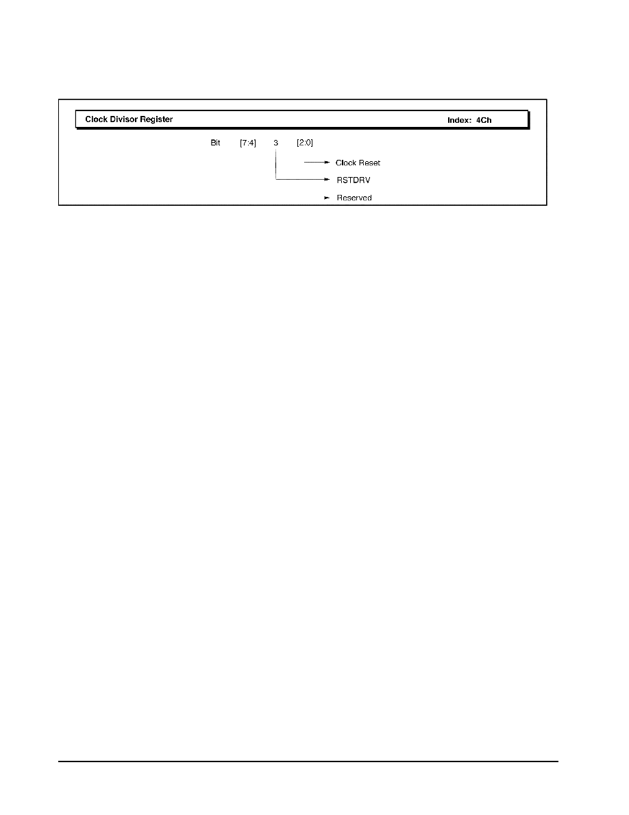
W83C553F Electrical Specifications
WINBOND SYSTEMS LABORATORY
66
Clock Divisor Register (default = 00h)
Type: Read/Write
Bit Description:
Bits [7:4]: Reserved.
Bit 3: RSTDRV. Reset Drive, valid only in PowerPC mode. When this bit is set, PCIRST# and
ISARST are enabled for 1 ms. This bit then clears (resets) itself.
Bits [2:0]: Clock select (CLKSEL). This field selects the divisor for generating BCLK from PCICLK.
Combinations not listed are reserved.
Bit 2 Bit 1 Bit 0
0 0 0 = 4
0 0 1 = 3
0 1 0 = 2
1 0 0 = 6
1 0 1 = 8
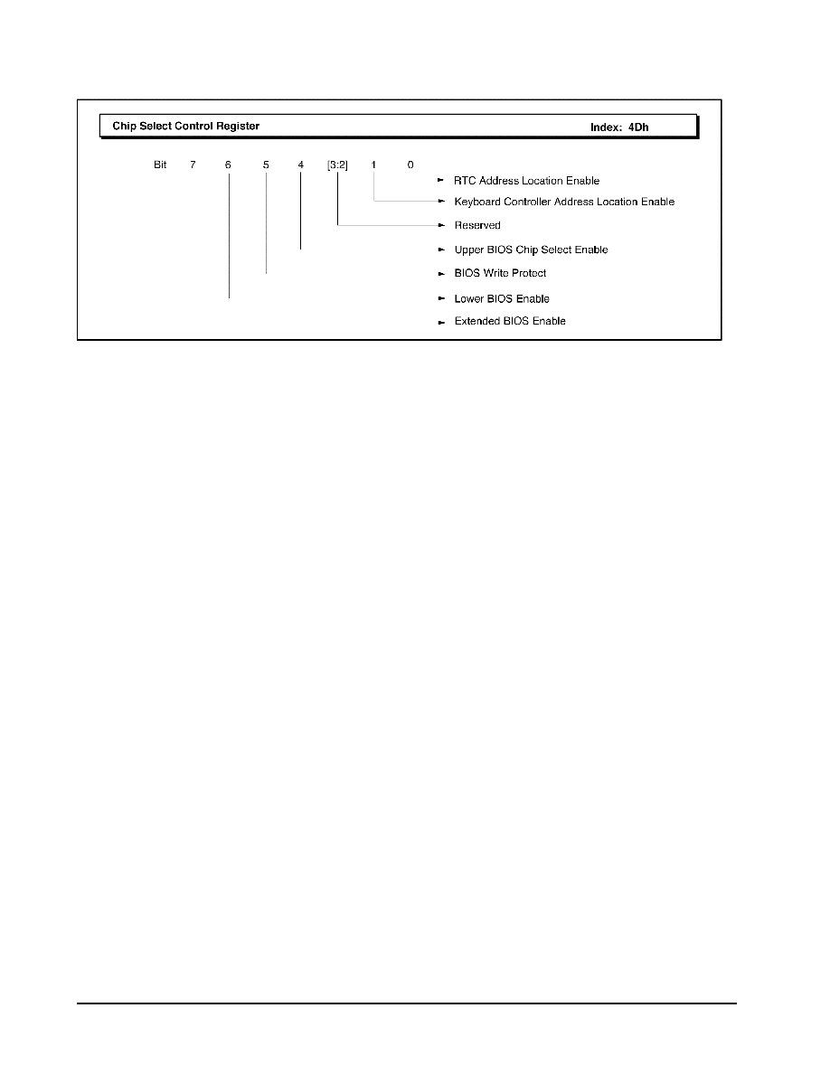
W83C553F Electrical Specifications
WINBOND SYSTEMS LABORATORY
67
Chip Select Control Register (default = 33h)
Type: Read/Write
Bit Description:
Bit 7: EBIOSCSE. Extended BIOS Enable.
0= Disabled
1= Memory access from FFF80000h to FFFDFFFFh will assert ROMCS in
PowerPC mode or the encoded output XCS[1:0 = 11 in x86 mode.
Bit 6: LBIOSCSE. Lower BIOS Enable.
0= Disabled
1= Memory access from FFFE,0000h to FFFE,FFFFh or FFEE,0000 to FFEE,FFFF
or 000E,0000 to 000E,FFFF will assert ROMCS in PowerPC mode or the
encoded output XCS[1:0] = 11 in x86 mode.
Bit 5: BIOSWP. BIOS Write Protect.
0= Disabled
1= When set, ROMCS in PowerPC mode or the encoded output XCS[1:0] = 11 in
x86 mode will not be generated for write access to the BIOS space.
Bit 4: UBIOSCSE. Upper BIOS Chip Select Enable. This bit defaults to "1" after reset.
0= Disabled
1= For Revision ID 0, Memory access from FFFF,0000h to FFFF,FFFFh or
FFEF,0000 to FFEF,FFFF or 000F,0000 to 000F,FFFF will assert ROMCS in
PowerPC mode or the encoded output XCS[1:0] = 11 in x86 mode.
For Revision ID 4, Memory access will be from 000F,0000 to 000F,FFFF or
FF80,0000 to FFFF,FFFF..
Bits [3:2]: Reserved.
Bit 1: KBCSE. Keyboard Controller Address Location Enable. .
0= Disabled
1= Access to the I/O ports 60h, 62h, 64h, or 66h will give the encoded output
XCS[1:0] = 11 for keyboard chip select in x86 mode. This bit is reserved in the
PowerPC mode.
Bit 0: RTCCSE. RTC Address Location Enable.
0= Disabled
1= Access to the I/O ports 70-77h will give the encoded output XCS[1:0] = 01 for for
RTC Data Port in x86 mode. This bit is reserved in the PowerPC mode.
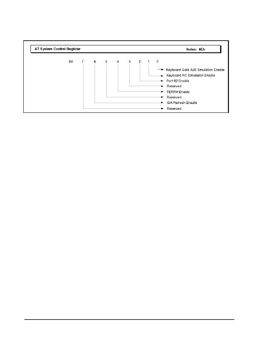
W83C553F Electrical Specifications
WINBOND SYSTEMS LABORATORY
68
AT System Control Register (default = 04h)
Type: Read/Write
Bit Description:
Bit 7: Reserved.
Bit 6: ISA Refresh Enable.
Bit 5: Reserved, always 0.
Bit 4: FERR# Enable. If this bit is set to "1," pin 12 will function as the Numeric Co-processor error
input.
Bit 3: Reserved.
Bit 2: P92E. Port 92 Enable. When enabled, access to Port 92 is enabled. When disabled, cycle will
be passed to the ISA bus.
Bit 1: Keyboard RC Emulation Enable. In x86 mode, this bit decodes the keyboard reset command
and generates INIT for at more than 4 PCI clocks. In PowerPC mode, this bit decodes the
keyboard reset command and generates HRESET# for 1ms.
Bit 0: Keyboard Gate A20 Emulation Enable. This bit toggles the Gate A20 output in x86 mode,
depending on the keyboard command.

W83C553F Electrical Specifications
WINBOND SYSTEMS LABORATORY
69
AT Bus Control Register (default = 00h)
Type: Read/Write
Bit Description:
Bits [7:3]: Reserved.
Bit 2: I/O Recovery Time.
0 = normal
1 = 4 BCLK delay for 16-bit I/O and 8 BCLK for 8-bit I/O access
Bit 1: Extended ALE.
0 = disable
1 = enable
Bit 0: Reserved.

W83C553F Electrical Specifications
WINBOND SYSTEMS LABORATORY
70
IRQ Break Event Enable 0 Register (default = 00h)
Function: This power management register may only be used while the W83C553F is in x86 mode.
Type: Read/Write
Bit Description:
Bit 7: IRQ7. Enable IRQ7 as Break Event. When this bit is "1," IRQ7 as Break Event detection is
enabled. Upon detection, PMACT# is de-asserted.
Bit 6: IRQ6. Enable IRQ6 as Break Event. When this bit is "1," IRQ6 as Break Event detection is
enabled. Upon detection, PMACT# is de-asserted.
Bit 5: IRQ5. Enable IRQ5 as Break Event. When this bit is "1," IRQ5 as Break Event detection is
enabled. Upon detection, PMACT# is de-asserted.
Bit 4: IRQ4. Enable IRQ4 as Break Event. When this bit is "1," IRQ4 as Break Event detection is
enabled. Upon detection, PMACT# is de-asserted.
Bit 3: IRQ3. Enable IRQ3 as Break Event. When this bit is "1," IRQ3 as Break Event detection is
enabled. Upon detection, PMACT# is de-asserted.
Bit 2: IRQ2. Enable IRQ2 as Break Event. When this bit is "1," IRQ2 as Break Event detection is
enabled. Upon detection, PMACT# is de-asserted.
Bit 1: IRQ1. Enable IRQ1 as Break Event. When this bit is "1," IRQ1 as Break Event detection is
enabled. Upon detection, PMACT# is de-asserted.
Bit 0: IRQ0. Enable IRQ0 as Break Event. When this bit is "1," IRQ0 as Break Event detection is
enabled. Upon detection, PMACT# is de-asserted.
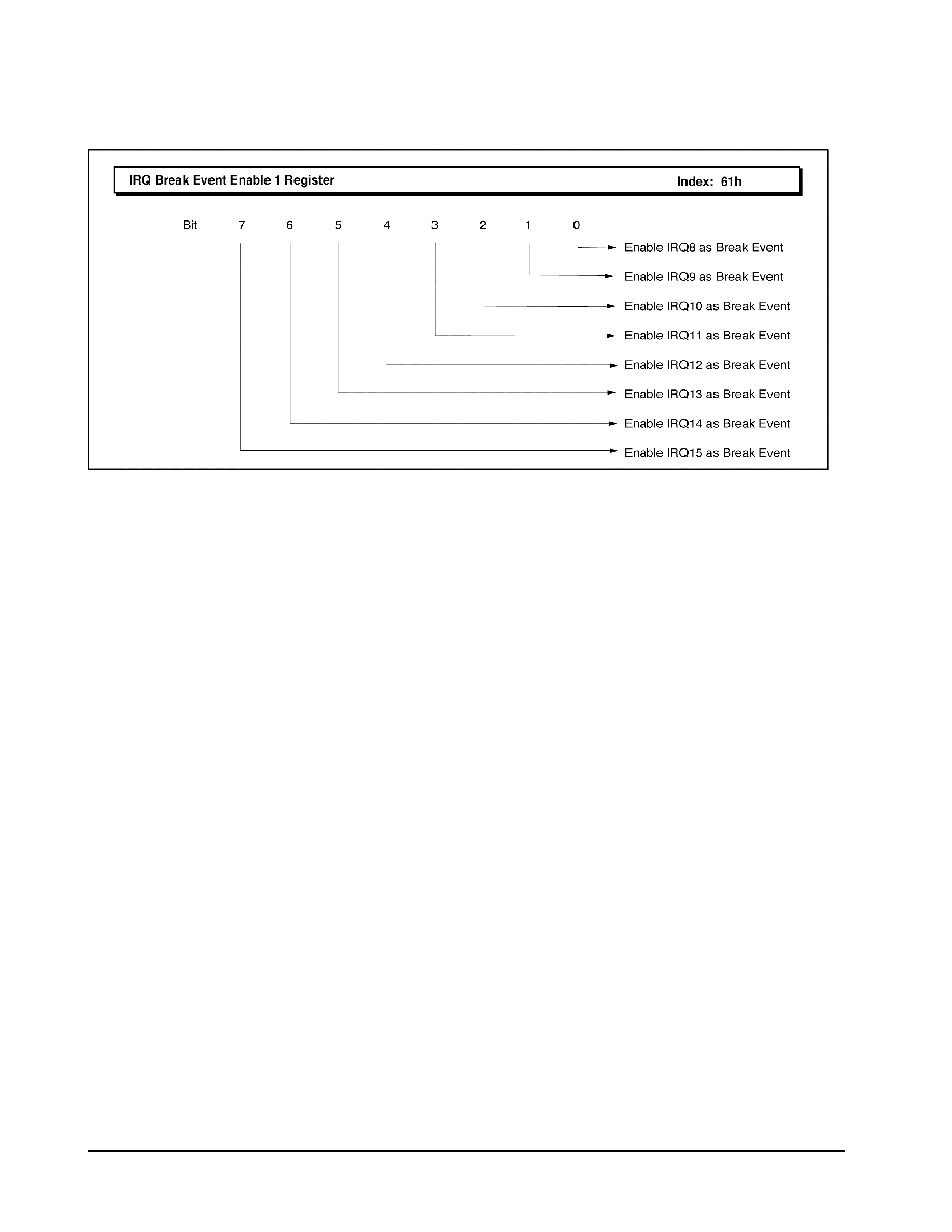
W83C553F Electrical Specifications
WINBOND SYSTEMS LABORATORY
71
IRQ Break Event Enable 1 Register (default = 00h)
Function: This power management register may only be used while the W83C553F is in x86 mode.
Type: Read/Write
Bit Description:
Bit 7: IRQ15. Enable IRQ15 as Break Event. When this bit is "1," IRQ15 as Break Event detection is
enabled. Upon detection, the PMU will de-assert PMACT#.
Bit 6: IRQ14. Enable IRQ14 as Break Event. When this bit is "1," IRQ14 as Break Event detection is
enabled. Upon detection, the PMU will de-assert PMACT#.
Bit 5: IRQ13. Enable IRQ13 as Break Event. When this bit is "1," IRQ13 as Break Event detection is
enabled. Upon detection, the PMU will de-assert PMACT#.
Bit 4: IRQ12. Enable IRQ12 as Break Event. When this bit is "1," IRQ12 as Break Event detection is
enabled. Upon detection, the PMU will de-assert PMACT#.
Bit 3: IRQ11. Enable IRQ11 as Break Event. When this bit is "1," IRQ11 as Break Event detection is
enabled. Upon detection, the PMU will de-assert PMACT#.
Bit 2: IRQ10. Enable IRQ10 as Break Event. When this bit is "1," IRQ10 as Break Event detection is
enabled. Upon detection, the PMU will de-assert PMACT#.
Bit 1: IRQ9. Enable IRQ9 as Break Event. When this bit is "1," IRQ9 as Break Event detection is
enabled. Upon detection, the PMU will de-assert PMACT#.
Bit 0: IRQ8. Enable IRQ8 as Break Event. When this bit is "1," IRQ8 as Break Event detection is
enabled. Upon detection, the PMU will de-assert PMACT#.
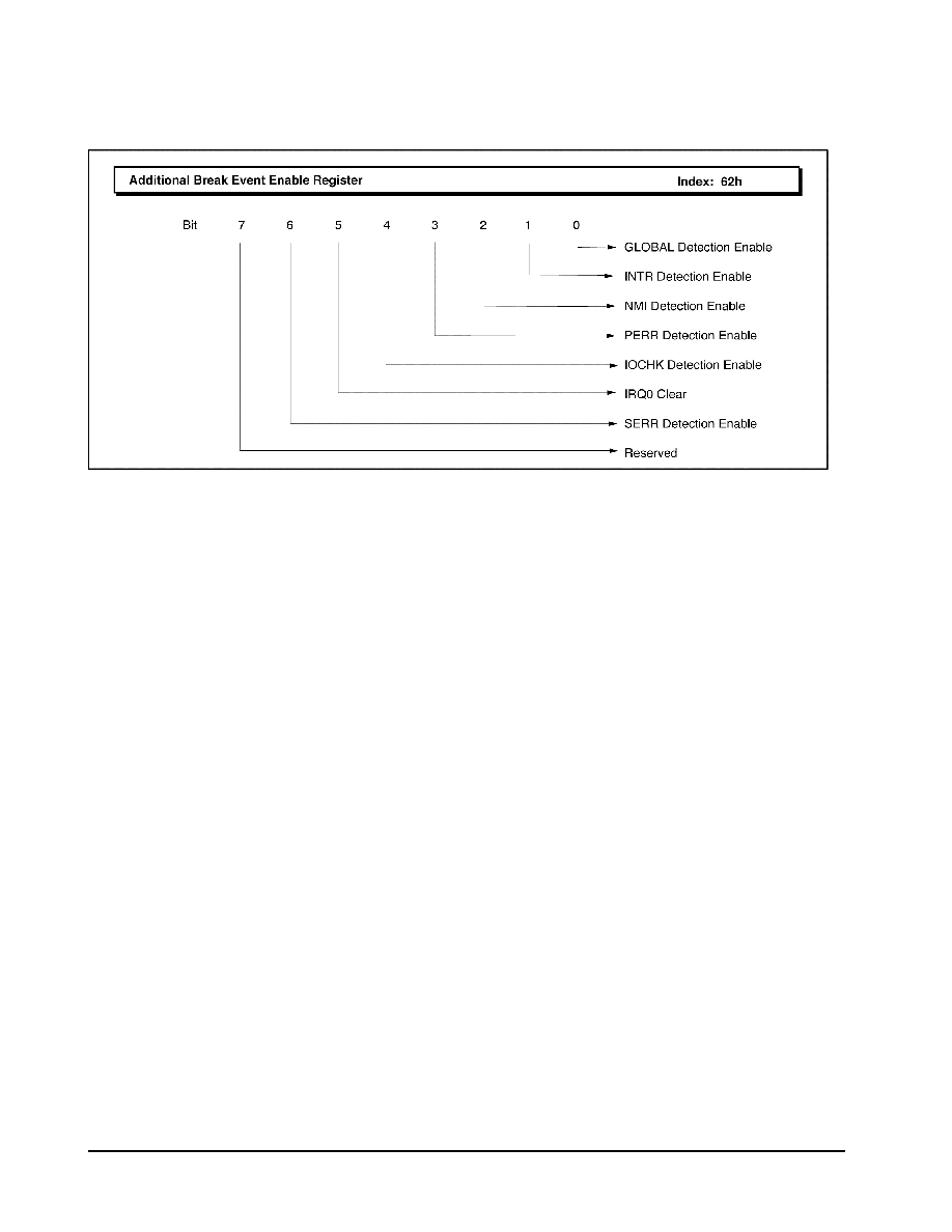
W83C553F Electrical Specifications
WINBOND SYSTEMS LABORATORY
72
Additional Break Event Enable Register (default = 00h)
Function: This power management register may only be used while the W83C553F is in x86 mode.
Type: Read/Write
Bit Description:
Bit 7: Reserved.
Bit 6: PCI SERR#. SERR Detection Enable. When this bit is "1," SERR detection is enabled. Upon
detection, the PMU will de-assert PMACT#.
Bit 5: IRQ0CLR. IRQ0 Clear. To clear IRQ0, write a "1", followed by a "0", to this bit.
Bit 4: ISA IOCHK#. IOCHK Detection Enable. When this bit is "1," IOCHK detection is enabled.
Upon detection, the PMU will de-assert PMACT#.
Bit 3: PCI PERR#. PERR Detection Enable. When this bit is "1," PERR detection is enabled. Upon
detection, the PMU will de-assert PMACT#.
Bit 2: NMI. NMI Detection Enable. When this bit is "1," NMI detection is enabled. Upon detection,
the PMU will de-assert PMACT#.
Bit 1: Interrupt. INTR Detection Enable. When this bit is "1," INTR detection is enabled. Upon
detection, the PMU will de-assert PMACT#.
Bit 0: PMUMGEN. GLOBAL Enable of Break Events. When this bit is "1," GLOBAL break event
detection is enabled. Upon detection, the PMU will de-assert PMACT#.
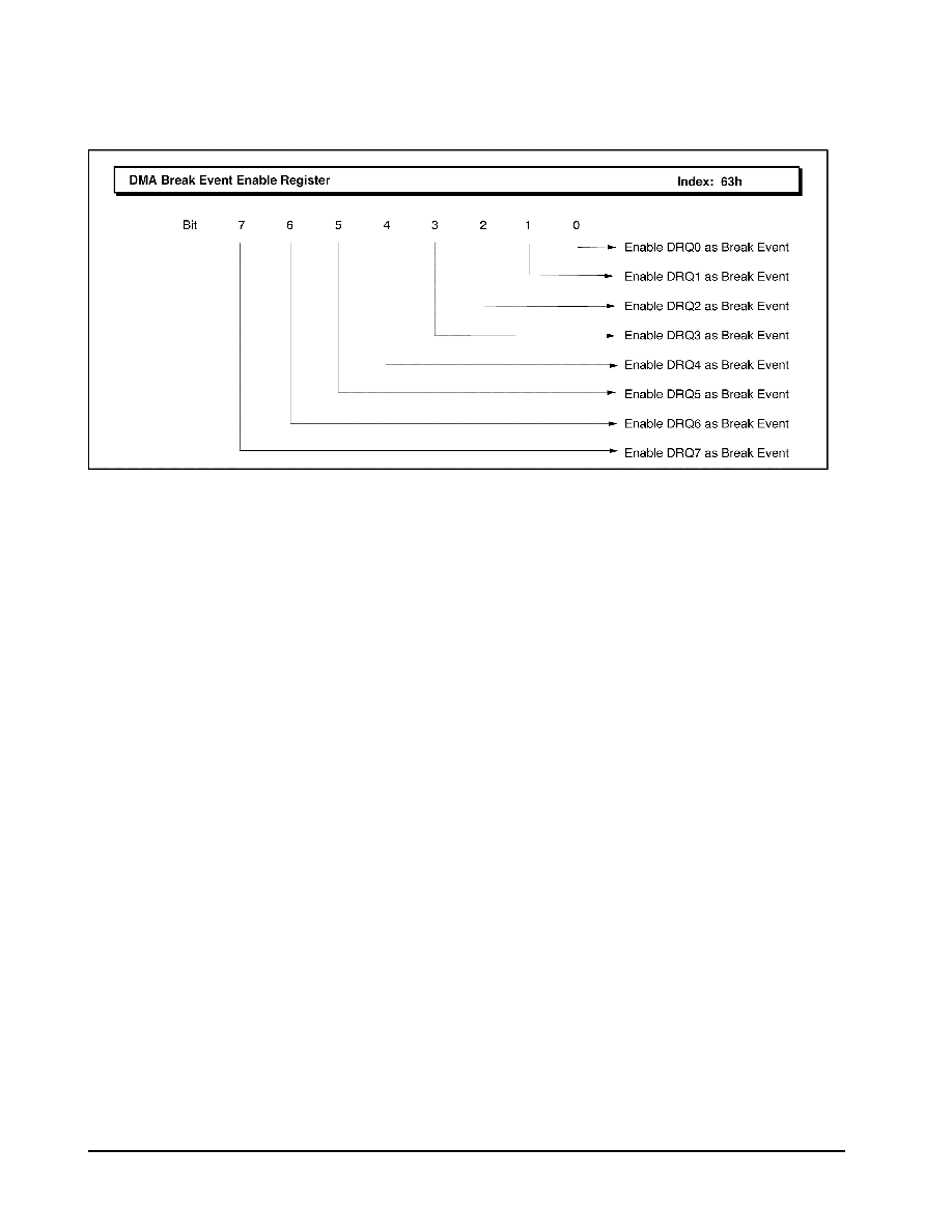
W83C553F Electrical Specifications
WINBOND SYSTEMS LABORATORY
73
DMA Break Event Enable Register (default = 00h)
Function: This power management register may only be used while the W83C553F is in x86 mode.
Type: Read/Write
Bit Description:
Bit 7: DRQ7. Enable DRQ7 as Break Event. When this bit is "1," DRQ7 detection is enabled. Upon
activation, the PMU will de-assert PMACT#.
Bit 6: DRQ6. Enable DRQ6 as Break Event. When this bit is "1," DRQ6 detection is enabled. Upon
activation, the PMU will de-assert PMACT#.
Bit 5: DRQ5. Enable DRQ5 as Break Event. When this bit is "1," DRQ5 detection is enabled. Upon
activation, the PMU will de-assert PMACT#.
Bit 4: DRQ4. Enable DRQ4 as Break Event. When this bit is "1," DRQ4 detection is enabled. Upon
activation, the PMU will de-assert PMACT#.
Bit 3: DRQ3. Enable DRQ3 as Break Event. When this bit is "1," DRQ3 detection is enabled. Upon
activation, the PMU will de-assert PMACT#.
Bit 2: DRQ2. Enable DRQ2 as Break Event. When this bit is "1," DRQ2 detection is enabled. Upon
activation, the PMU will de-assert PMACT#.
Bit 1: DRQ1. Enable DRQ1 as Break Event. When this bit is "1," DRQ1 detection is enabled. Upon
activation, the PMU will de-assert PMACT#.
Bit 0: DRQ0. Enable DRQ0 as Break Event. When this bit is "1," DRQ0 detection is enabled. Upon
activation, the PMU will de-assert PMACT#.
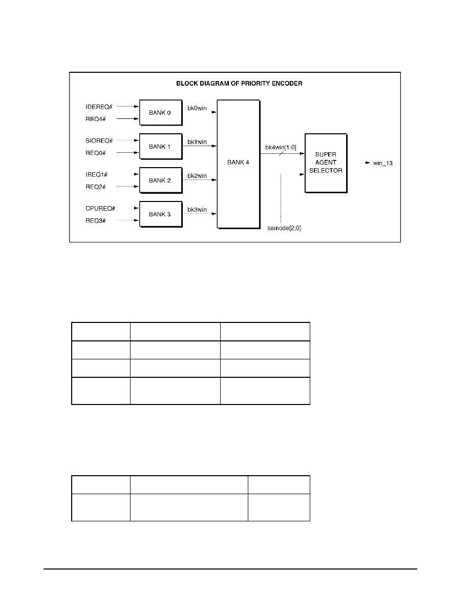
W83C553F Electrical Specifications
WINBOND SYSTEMS LABORATORY
74
Level 1 Arbiter
There are two control bits for bank 1,2,3 modules. The "pfix" bit determines the fixed priority of the bank. The "protat" bit
determines whether to rotate the priority scheme of the bank after a grant is given. If the "protat" bit is not set, the arbiter will
give one request line higher priority ALL THE TIME. If the "protat" bit is set, the priority of the request lines are rotated
after each grant to the higher priority line. For bank 0, the "pfix" value is fixed to 0 and the "protat" value is fixed to 0 also.
pfix = 0
pfix = 1
Bank 1
SIOREQ# > REQ0#
REQ0# > SIOREQ#
Bank 2
REQ1# > REQ2#
REQ2# > REQ1#
Bank 3
CPUREQ# > REQ3#
REQ3# > CPUREQ#
Level 2 Arbiter
For bank 4, there are 2 bits, "fpmod[1:0]", indicating the fixed priority of the bank. There is one bit, "bk4rc", controlling the
rotation of priority schemes. There are a total of 4 priority schemes each. A total of 8 slots are available on the round-robin
rotation. 4 slots are assigned with a priority scheme each. 4 other slots are programmable with selected priority schemes.
fpmod[1:0]
Priority Schemes
Slots
00
IDEREQ# > bk1win > bk3win
Bank 0
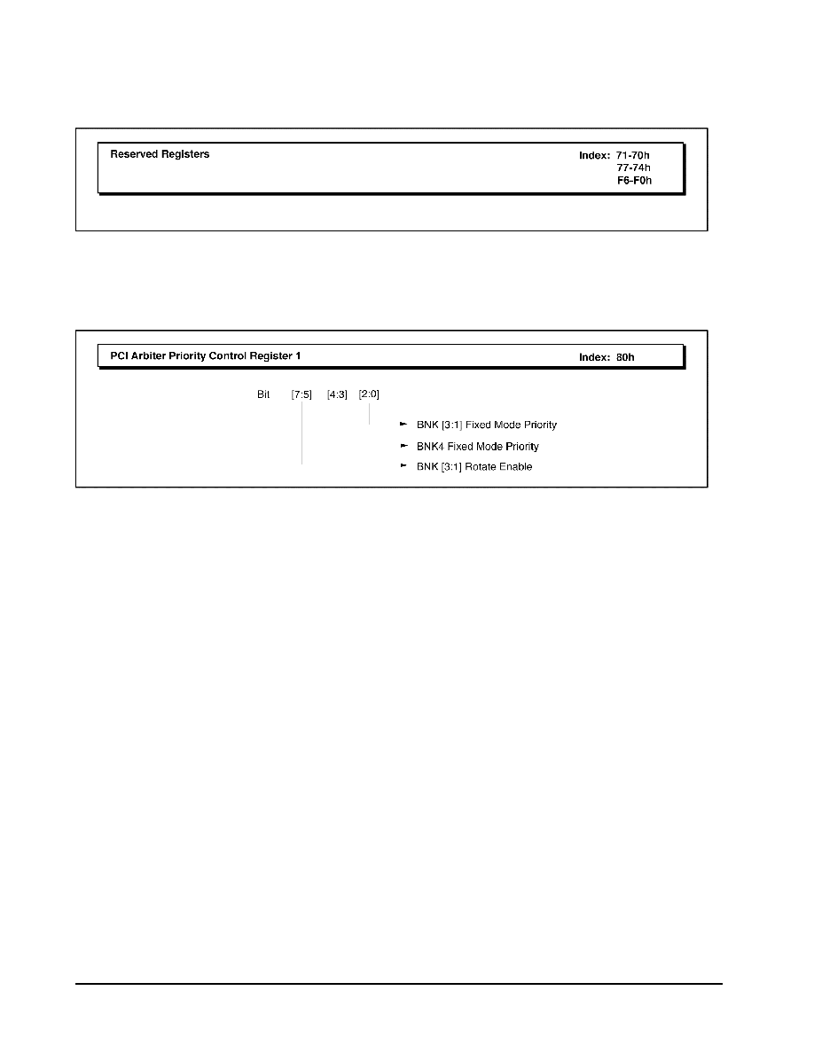
W83C553F Electrical Specifications
WINBOND SYSTEMS LABORATORY
75
Function: These register locations are reserved. Software should not attempt to read or write these locations.
PCI Arbiter Priority Control Register 1 (default = E0h)
Type: Read/Write
Bit Description:
Bits [7:5]: Bank [3:1] Rotate Enable. Defaults to 111b (enabled).
Bits [4:3]: Bank 4 Fixed Mode Priority Select.
Bit 4 3 Function
0 0 ide �> bk1 �> bk2 �> bk3
0 1 bk1 �> bk2 �> bk3 �> ide
1 0 bk2 �> bk3 �> ide �> bk1
1 1 bk3 �> ide �> bk1 �> bk2
Bits [2:0]: Bank [3:1] Fixed Mode Priority Select. If 0 upper ones will be chosen, IDEIRQ# priority always
higher than REQ4#
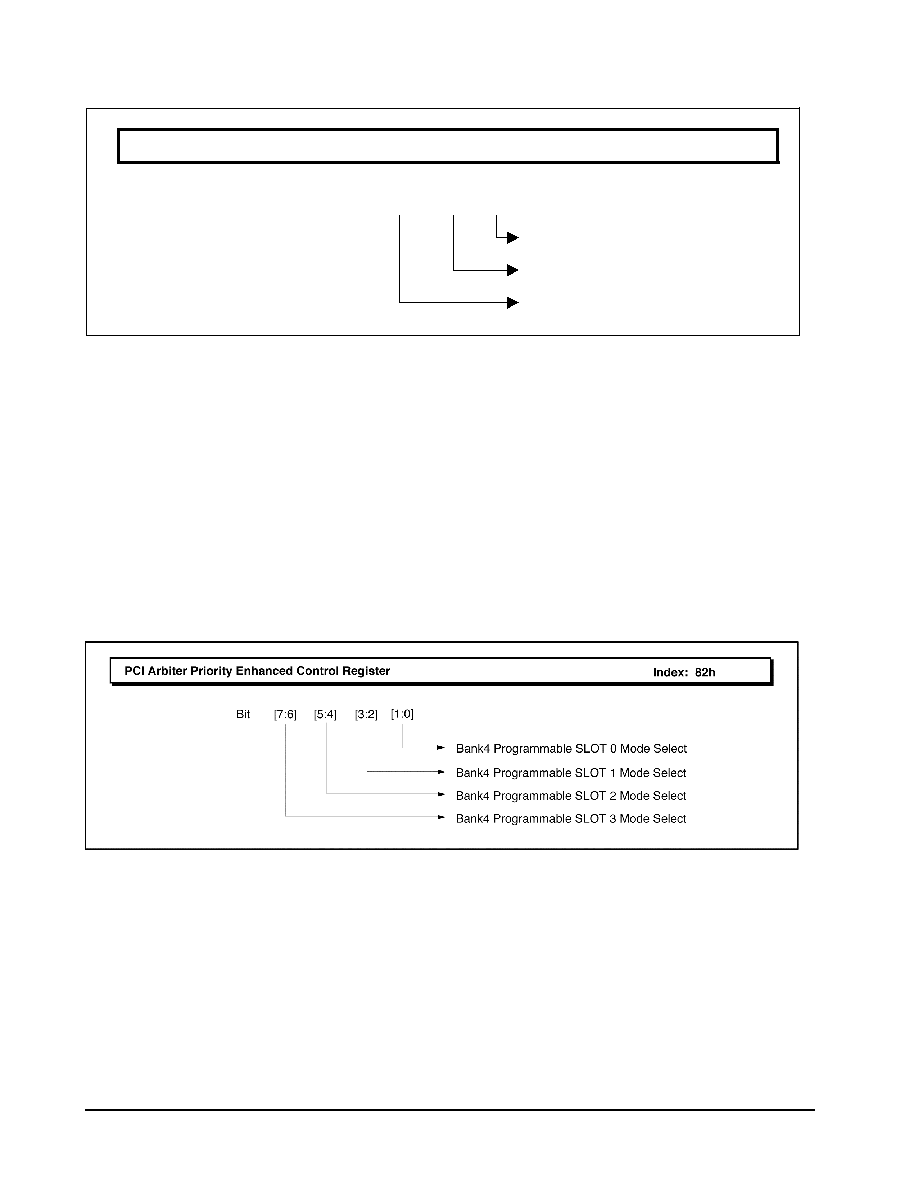
W83C553F Electrical Specifications
WINBOND SYSTEMS LABORATORY
76
PCI Arbiter Priority Extension Control Register (default = 01h)
Type: Read/Write
Bit Description:
Bits [7:4]: Reserved
Bits [3:1]: Super Agent Select [2:0].
000 DISABLE 100 REQ0#
001 IDEIRQ# 101 REQ1#
010 SIOIRQ# 110 REQ2#
011 CPUREQ# 111 REQ3#
Bits 0: Bank 4 Rotate Enable. Defaults to 1b (enabled).
PCI Arbiter Priority Enhanced Control Register (default = 00h)
Type: Read/Write
Bit Description:
Bits [7:6]: Bank 4 Programmable Slot 3 Select [1:0].
Bits [5:4]: Bank 4 Programmable Slot 2 Select [1:0].
Bits [3:2]: Bank 4 Programmable Slot 1 Select [1:0].
Bits [1:0]: Bank 4 Programmable Slot 0 Select [1:0].
PCI Arbiter Priority Extension Control Register Index: 81h
Bit [7:4] [3:1] 0
BNK4 Rotary Enable
SAGENT Select [2:0]
Reserved
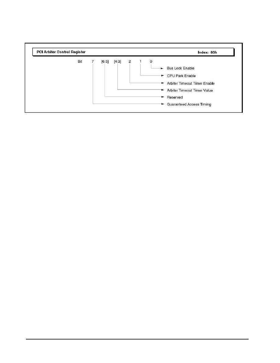
W83C553F Electrical Specifications
WINBOND SYSTEMS LABORATORY
77
PCI Arbiter Control Register (default = 80h)
Type: Read/Write
Bit Description:
Bit 7: GAT. Guaranteed Access Timing. If set to a 1b, this bit enables Function 0 Flush Request and
Flush Acknowledge operation on pins 6 and 7 (provided pin 13 is not pulled low after reset).
This bit defaults to a 1b.
Bit [6:5]: Reserved.
Bits [4:3]: Arbiter Timeout Timer Value [2:0]
Number of clocks to wait for FRAME# to asset after GNT# is asserted
00 ATO time out after 16 clocks
01 ATO time out after 4 clocks
10 ATO time out after 8 clocks
11 ATO time out after 32 clocks
Bit 2: Arbiter Timeout Timer Enable.
Bit 1: CPU Park Enable. Otherwise the arbiter will park on the last master. 0=Enable.
Bit 0: Bus Lock Enable. If set to 1b, this bit converts a PCI Lock cycle to a bus lock. If this bit is 0b,
the PCI arbiter ignores the LOCK# signal on the PCI bus.
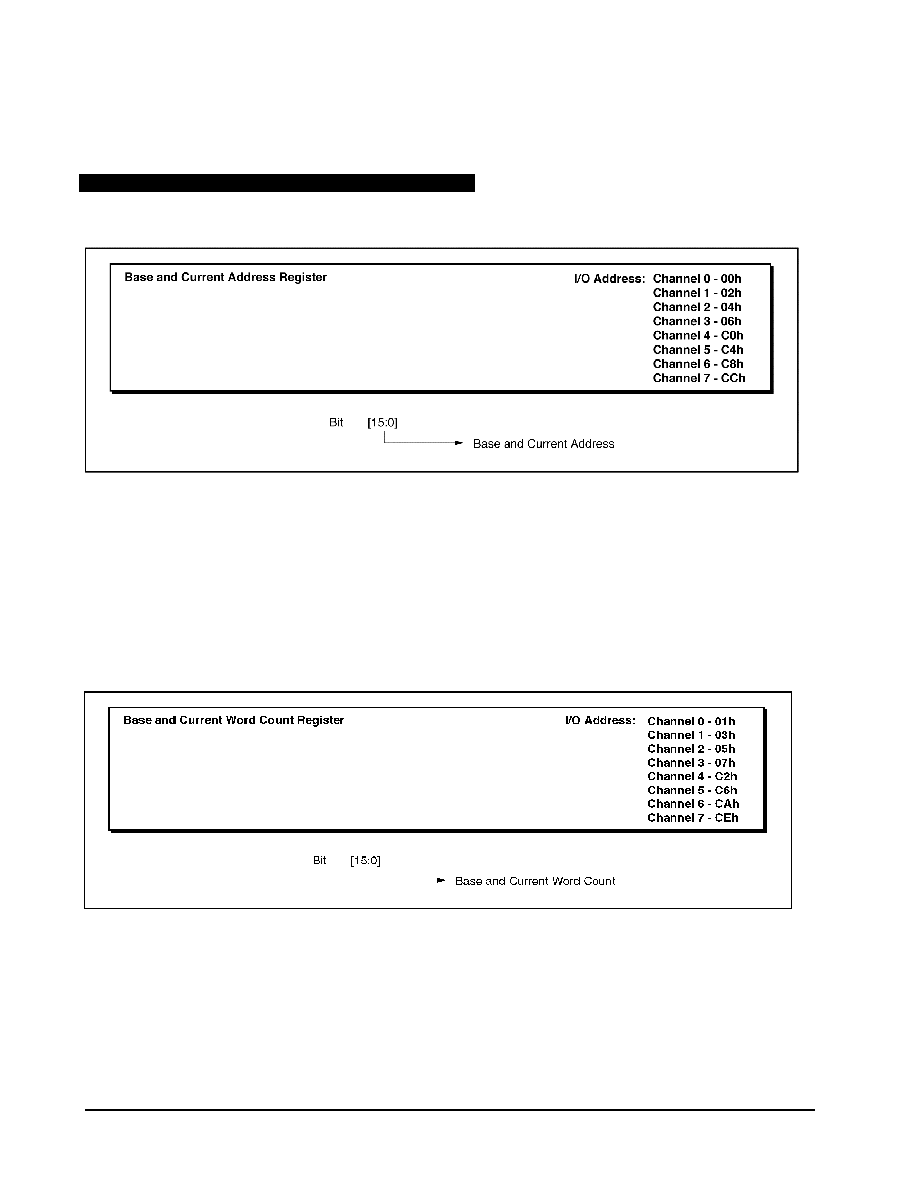
W83C553F Electrical Specifications
WINBOND SYSTEMS LABORATORY
78
4.2 ISA Bridge (Function 0) I/O Registers
4.2.1 DMA Controller I/O Registers
Base and Current Address Register
Type: Read/Write
Bit Description:
Bits [15:0]: Base and Current Address. Access by two consecutive cycles. Internal high/low byte pointer
toggles after each access.
Base and Current Word Count Register
Type: Read/Write
Bit Description:
Bits [15:0]: Base and Current Word Count. Access by two consecutive cycles. Internal high/low byte
pointer toggles after each access.

W83C553F Electrical Specifications
WINBOND SYSTEMS LABORATORY
79
DMA Command Register (default = 00h)
Type: Write only
Bit Description:
Bit 7: Reserved.
Bit 6: DRQ Active Level. When this bit is "0" (default), DRQ is active high. When this bit is "1," DRQ
is active low.
Bit 5: Reserved. Extended/Late Write Select. Must be "0".
Bit 4: Priority Scheme.
0 = fixed.
1 = rotating.
Bit 3: Reserved. Compressed timing. Must be "0".
Bit 2: Controller Enable. (0=Enable; 1=Disable)
Bits [1:0]: Reserved. Memory-to-Memory Transfer Control. Must be "0".
W83C553F Electrical Specifications
WINBOND SYSTEMS LABORATORY
80
DMA Controller 1 Status Register (default = 00h)
Type: Read only
Bit Description:
Bit 7: Channel 3 Request.
Bit 6: Channel 2 Request.
Bit 5: Channel 1 Request.
Bit 4: Channel 0 Request.
Bit 3: Channel 3 Terminal Count.
Bit 2: Channel 2 Terminal Count.
Bit 1: Channel 1 Terminal Count.
Bit 0: Channel 0 Terminal Count.
W83C553F Electrical Specifications
WINBOND SYSTEMS LABORATORY
81
DMA Controller 2 Status Register
Type: Read only
Bit Description:
Bit 7: Channel 7 Request.
Bit 6: Channel 6 Request.
Bit 5: Channel 5 Request.
Bit 4: Reserved. Cascade for DMA Controller 1.
Bit 3: Channel 7 Terminal Count.
Bit 2: Channel 6 Terminal Count.
Bit 1: Channel 5 Terminal Count.
Bit 0: Reserved. Cascade for DMA Controller 1.
W83C553F Electrical Specifications
WINBOND SYSTEMS LABORATORY
82
DMA Controller Request Register
Type: Write only
Bit Description:
Bits [7:3]: Reserved.
Bit 2: Set Request.
Bits [1:0]: Channel Select.
DMA Controller Mask Register
Type: Write only
Bit Description:
Bits [7:3]: Reserved.
Bit 2: SETMASK. Set Mask bit.
Bits [1:0]: CSEL [1:0]. Channel Select bits.

W83C553F Electrical Specifications
WINBOND SYSTEMS LABORATORY
83
DMA Controller Mode Register
Type: Write only
Bit Description:
Bits [7:6]: Transfer Mode.
Bit 7 Bit 6
0 0 = Demand Mode
0 1 = Single Mode
1 0 = Block Mode
1 1 = Cascade Mode
Bit 5: Decrement Address. When set to "1", address pointer is decremented after each transfer.
Default is incrementing address.
Bit 4: Auto initialize Enable.
Bits [3:2]: Transfer Type.
Bit 3 Bit 2
0 0 = Verify
0 1 = Write
1 0 = Read
1 1 = Illegal Type
Bits [1:0]: Channel Select.
W83C553F Electrical Specifications
WINBOND SYSTEMS LABORATORY
84
Clear Byte Pointer Register
Type: Write only
Bit Description:
Bits [7:0]: Clear Byte Pointer. Writing any pattern in this register will reset the byte pointer for the Base
and Current Address/Data registers.
Master Clear Register
Type: Write only
Bit Description:
Bits [7:0]: Master Clear. Writing any pattern in this register will initialize the DMA controller to the same
state as in a hardware reset.
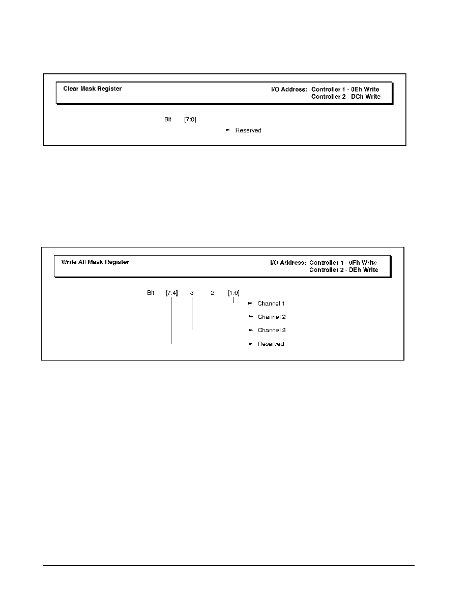
W83C553F Electrical Specifications
WINBOND SYSTEMS LABORATORY
85
Clear Mask Register
Type: Write only
Bit Description:
Bits [7:0]: Reserved. Writing this register will clear the mask bits of all channels.
Write All Mask Register (default = 0Fh)
Type: Write only
Bit Description:
Bits [7:4]: Reserved.
Bit 3: Channel 3
Bit 2: Channel 2
Bit 1: Channel 1
Bit 0: Channel 0 0 enable, 1 mask
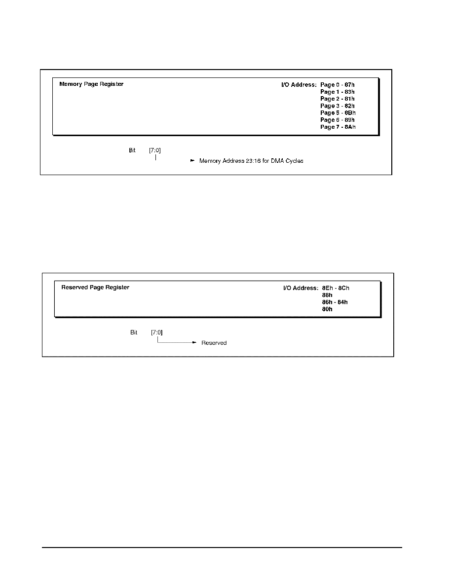
W83C553F Electrical Specifications
WINBOND SYSTEMS LABORATORY
86
Memory Page Register (default = 00h)
Type: Read/Write
Bit Description:
Bits [7:0]: Memory Address [23:16] for DMA cycles.
Reserved Page Register
Bit Description:
Bits [7:0]: Reserved. Software should not attempt to access these registers.
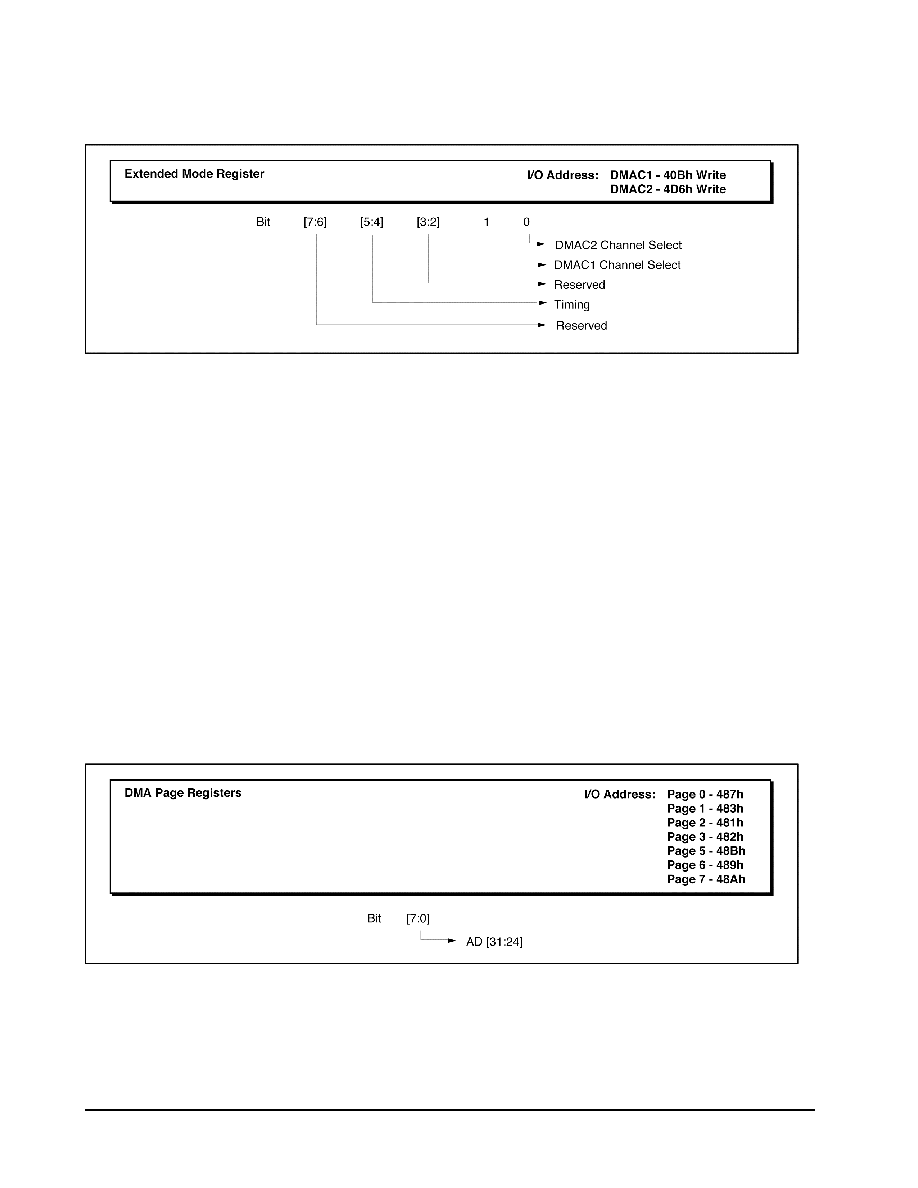
W83C553F Electrical Specifications
WINBOND SYSTEMS LABORATORY
87
Extended Mode Register (default = 0xh)
Type: Write only
Bit Description:
Bits [7:6]: Reserved.
Bits [5:4]: Timing.
Bit 5 Bit 4
0 0 Compatible Timing
0 1 A
1 0 B
1 1 F Note: IOR# is 1 BCLK wide for IO to Memory DMA
Note: IOW# is 3-5BCLK wide for Memory to IO DMA
Bits [3:2]: Reserved.
Bits [1:0] DMAC[1:0] Channel Select.
DMAC1 DMAC2
Bit 1 Bit 0 Channel Select Channel Select
0 0 0 Reserved
0 1 1 5
1 0 2 6
1 1 3 7
DMA Page Registers (default = 00h)
Type: Read/Write
Bit Description:
Bits [7:0]: AD[31:24].

W83C553F Electrical Specifications
WINBOND SYSTEMS LABORATORY
88
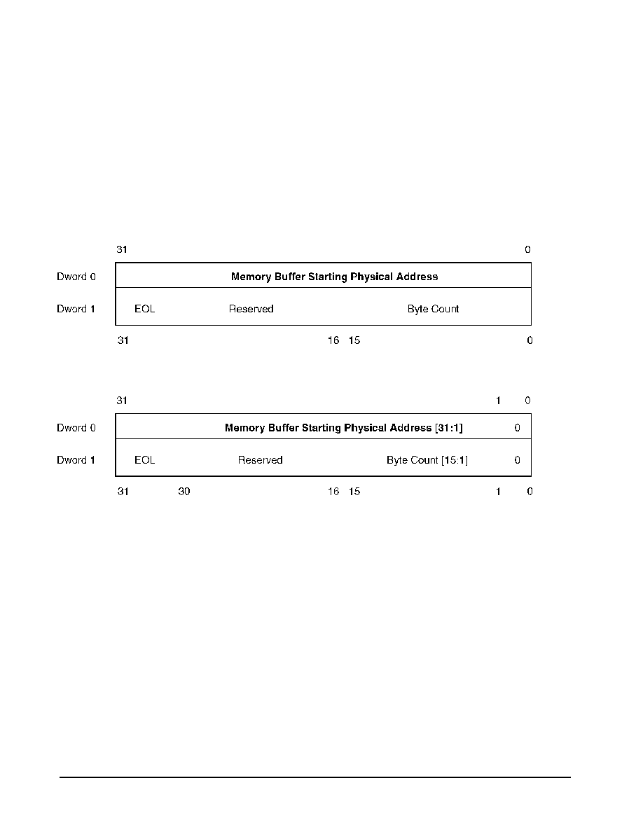
W83C553F Electrical Specifications
WINBOND SYSTEMS LABORATORY
89
Scatter/Gather Registers
Scatter/Gather (S/G) provides the capability of transferring multiple buffers between memory (ISA/PCI) and I/O (ISA DMA
device) without CPU intervention. In Scatter/Gather the DMA can read the memory address and word count from an array of
buffer descriptors located in system memory (PCI only), called the Scatter/Gather Descriptor (SCD) table. This allows the
DMA controller to sustain DMA transfers until all of the buffers in the SGD table are transferred.
Software prepares a SGD table in system memory. Each SGD is 8-bytes long and consists of an address pointer to the
starting address and the byte count (number of bytes) of the memory buffer to be transferred. In any given SGD table, two
consecutive SGDs are offset by 8-bytes and are aligned on a 4-byte boundary. Each SGD is defined below. For an 8-bit
DMA I/O device:
For a 16-bit DMA I/O device, bit 0 of the Memory Buffer Starting Address and byte count must be 0.
Bit 31 of Dword 1 is the end of Link Flag. Bus master operation terminates upon completion of the description entry that has
EOL set.
The SGD table cannot cross a 64k memory boundary.
The addresses of all of the registers located from 43Fh to 40Ah (except 40Bh) are relocatable by programming the
Scatter/Gather Relocation Base Address Register (Function 0, address 41h) in the PCI Configuration Space. These registers
are marked with an asterisk (*).

W83C553F Electrical Specifications
WINBOND SYSTEMS LABORATORY
90
Scatter/Gather Interrupt Status Register (default = 00h)
Type: Read only
Bit Description:
Bits [7:5]: Channel [7:5] Interrupt Status. When one of these bits is set to a 1b, Channels 7 through 5
have an interrupt due to a Scatter/Gather transfer; otherwise these bits are set to 0b.
Bit [4] Reserved
Bits [3:0]: Channel [3:0] Interrupt Status. When one of these bits is set to a 1b, Channels 3 through 0
have an interrupt due to a Scatter/Gather transfer; otherwise these bits are set to 0b.
Scatter/Gather Interrupt Status Register I/O Address: 40Ah Read
Bit [7:5] 4 [3:0]
Channel Interrupt
Reserved
Channel Interrupt
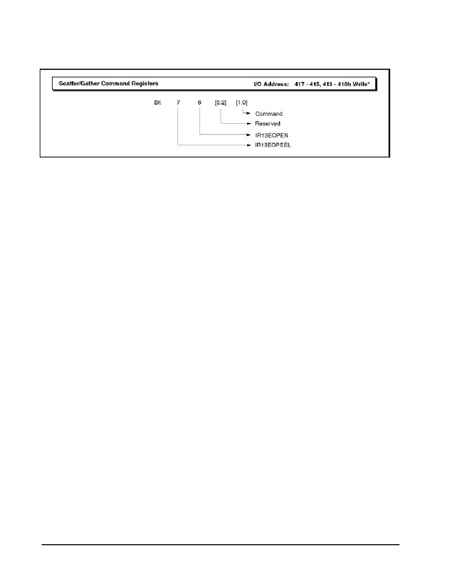
W83C553F Electrical Specifications
WINBOND SYSTEMS LABORATORY
91
Scatter/Gather Command Registers (default = 000000h)
Function: Each of these three registers controls the Scatter/Gather operation of DMA channels [7:5].
Type: Write only
Bit Description:
Bit 7: IR13EOPSEL. IRQ13/EOP Select. If enabled via bit 6 of this register, bit 7 selects whether
EOP or IRQ13 is asserted at termination caused by a last buffer expiring. If bit 7 = 1, EOP is
asserted; otherwise IRQ13 is asserted.
Bit 6: IRQ13EOPEN. IRQ13/EOP Programming Enable. If bit 6 = 1, it enables IRQ13/EOP
programming and allows initialization or modification of the Scatter/Gather termination handling
bits.
Bits [5:2]: Reserved. Must be 0.
Bits [1:0]: Scatter/Gather Commands.
Bit 1 0 Command
0 0 No Scatter/Gather operation.
0 1 Start Scatter/Gather.
1 0 Stop Scatter/Gather. This will halt a transfer immediately.
1 1 Reserved.
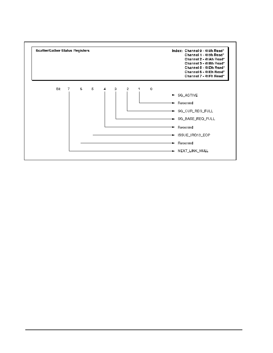
W83C553F Electrical Specifications
WINBOND SYSTEMS LABORATORY
92
Scatter/Gather Status Registers
Type: Read only
Bit Description:
Bit 7: NEXT_LINK_NULL. Next Link Null Indicator.
Bit 6: Reserved.
Bit 5: ISSUE_IRQ13_EOP. Issue IRQ13 on last buffer. When bit 5 = 0, EOP is issued on last buffer;
when bit 5 = 1, IRQ13 is issued.
Bit 4: Reserved.
Bit 3: SG_BASE_REQ_FULL. Scatter/Gather Base Register Status. When bit 3 = 0, the base
register is empty; when bit 3 = 1, the base register has a buffer link loaded.
Bit 2: SG_CUR_REG_FULL. Scatter/Gather Current Register Status. When bit 2 = 0, the current
register is empty; when bit 2 = 1, the current register has a buffer link loaded.
Bit 1: Reserved.
Bit 0: SG_ACTIVE. Scatter/Gather Active. This bit indicates the current Scatter/Gather transfer
status. Bit 0 is set to 1 after a Scatter/Gather Start Command is issued. When bit 0 = 0, it
means there is no Scatter/Gather operation.
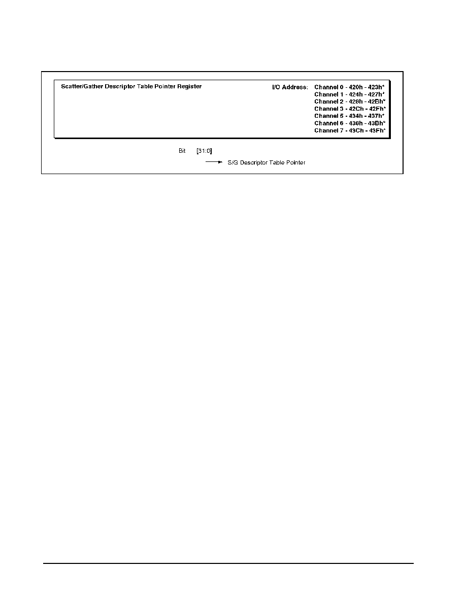
W83C553F Electrical Specifications
WINBOND SYSTEMS LABORATORY
93
Scatter/Gather Descriptor Table Pointer Register
Type: Read/Write
Bit Description:
Bits [31:0]: SG_TBL_PTR. The Scatter/Gather Descriptor Table Pointer Register contains a 32-bit pointer
address to the main memory location where the software maintains the Scatter/Gather
descriptors for the linked-list buffers. Bits [31:0] correspond to A[31:0] on the PCI AD bus.
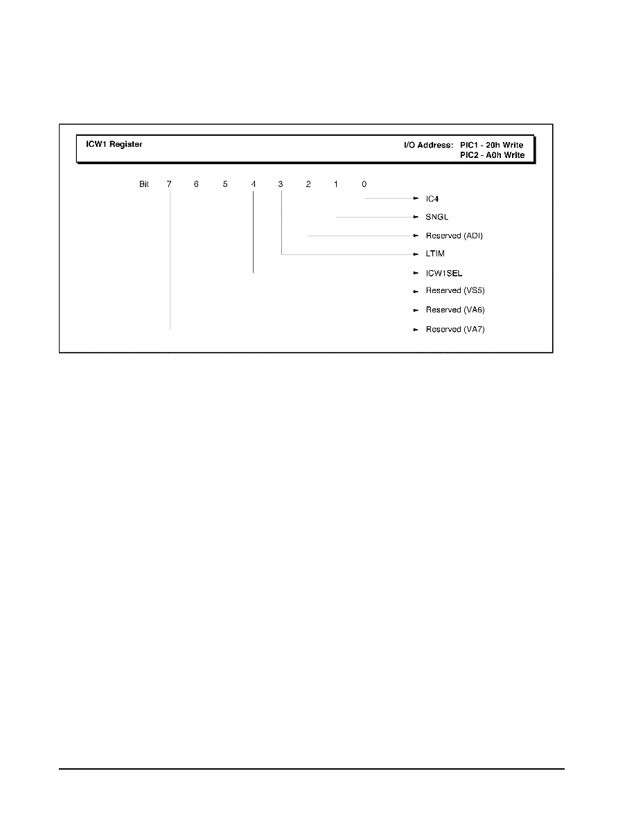
W83C553F Electrical Specifications
WINBOND SYSTEMS LABORATORY
94
4.2.2 Programmable Interrupt Controller (PIC) Registers
Initialization Command Word 1 Register (default = 19h)
Function: A write to the Initialization Command Word 1 (ICW1) Register starts the interrupt controller
initialization sequence. Addresses 20h and A0h are referred to as the base address of Interrupt
Controllers #1 and #2 respectively. An I/O write to the Interrupt Controller #1 or #2 base address, with
bit 4 equal to "1," is interpreted as ICW1. For W83C553F based ISA systems, three I/O writes to "base
address +1" must follow the ICW1 to perform writes to ICW2, ICW3 and ICW4.
Type: Write Only
Bit Description:
Bits [7:5]: Reserved. These bits are not needed by the W83C553F and should be "000" while
programming.
Bit 4: ICW1SEL. This bit must be a "1" to select ICW1. After the fixed initialization sequence to
ICW1, ICW2, ICW3 and ICW4, the controller base address is used to write to OCW2 and
OCW3. Bit 4 is "0" on writes to these registers.
Bit 3: LTIM. This bit is always ignored and read as a "1."
Bit 2: Reserved (ADI). This bit is ignored by the W83C553F.
Bit 1: SNGL. This bit must be programmed to a "0," indicating the two interrupt controllers are
operating in cascade mode.
Bit 0: IC4. ICSW4 Write Required. This bit must be set to a "1," indicating the ICW4 needs to be
programmed (that is, the controllers are operating in an x86 type system).

W83C553F Electrical Specifications
WINBOND SYSTEMS LABORATORY
95
Operational Control Word 2 Register
Function: The Operational Control Word 2 (OCW2) Register controls both the Rotate Mode, End of Interrupt
Mode and combinations of the two.
Type: Write Only
Bit Description:
Bits [7:5]: ROT, SELLEVEL and EOI. These three bits control the Rotate, End of Interrupt (EOI) Modes
and combinations of the two, as shown below:
Bit 7 Bit 6 Bit 5 Mode
0 0 0 Rotate in Automatic EOI Mode (clear).
0 0 1 Non-specific EOI command
0 1 0 No operation
0 1 1 Specific EOI command
1 0 0 Rotate in Automatic EOI Mode (set)
1 0 1 Rotate on non-specific EOI command
1 1 0 *Set Priority Command
1 1 1 *Rotate on specific EOI command
*Level 0 - Level 2 are used (bits [2:0])
Bits [4:3]: OCW2SEL[1:0]. OCW2 Selects. When selecting OCW2, these bits must be "00." If bit 4 is
"1," the interrupt controller interprets the write to this port as an ICW1.
Bits [2:0]: LEVEL[2:0]. These bits determine the interrupt level acted upon when the SC bit (6) is active,
as shown below.
Bit 2 Bit 1 Bit 0 Interrupt Level
0 0 0 IRQ0 (8)
0 0 1 IRQ1 (9)
0 1 0 IRQ2 (10)
0 1 1 IRQ3 (11)
1 0 0 IRQ4 (12)
1 0 1 IRQ5 (13)
1 1 0 IRQ6 (14)
1 1 1 IRQ7 (15)
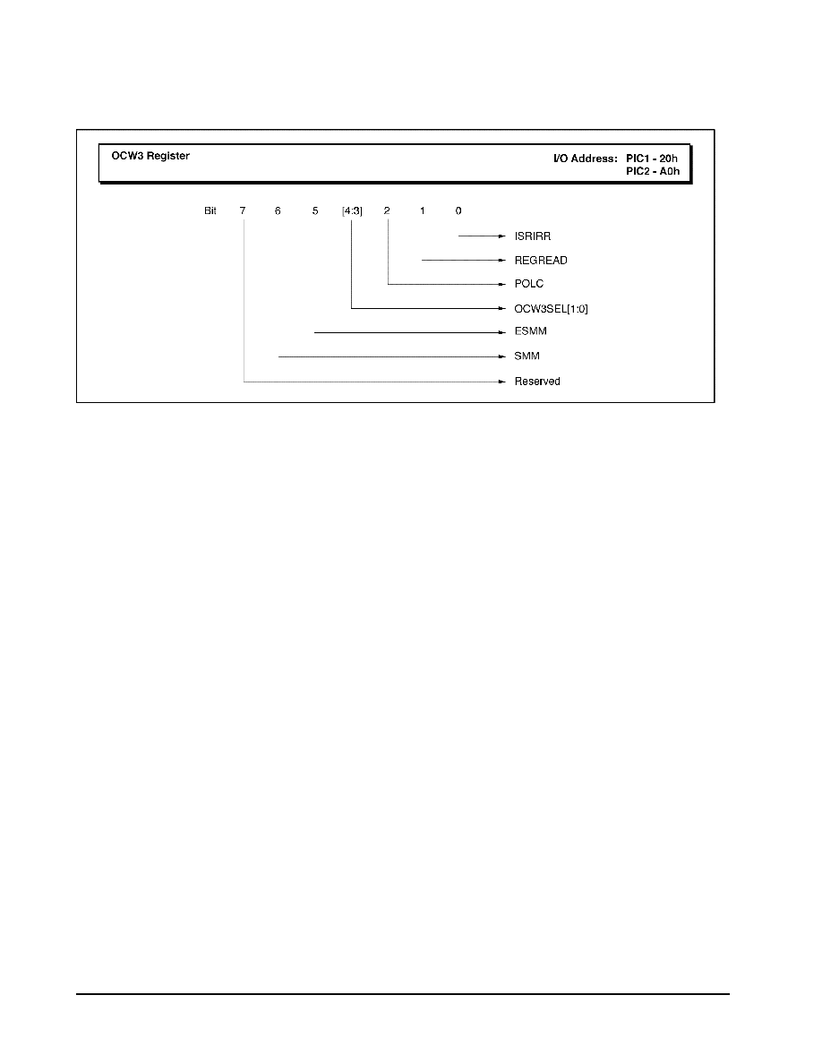
W83C553F Electrical Specifications
WINBOND SYSTEMS LABORATORY
96
Operational Control Word 3 Register
Function: The Operational Control Word 3 (OCW3) Register serves three functions. It enables special mask mode
and controls poll mode and IRR/ISR register read.
Type: Read/Write
Bit Description:
Bit 7: Reserved. This bit must be "0."
Bit 6: SMM. Special Mask Mode. If ESMM and SMM are both "1," the interrupt controller enters
SMM. If ESMM is "1" and SMM is "0," the interrupt controller is in normal mask mode. When
ESMM is "0," SMM has no effect.
Bit 5: ESMM. Enable Special Mask Mode. If ESMM is "1," the SMM bit is enabled to set or reset
Special Mask Mode. If ESMM is "0," the SMM bit is a "don't care."
Bits [4:3]: OCW3SEL[1:0]. OCW3 Select. Always ensure bit 4 is "0" and bit 3 is "1" when writing an
OCW3.
Bit 2: POLC. When this Poll Mode Command bit is "0," the Poll Command is not issured. When this
bit is "1," the next I/O read to the interrupt controller is treated as an interrupt acknowledge
cycle.
Bits [1:0]: REGREAD and ISRIRR. These Register Read Command bits provide control for reading the
In-Service Register (ISR) and Interrupt Request Register (IRR), as shown below.
Bit 1 Bit 0 Function
0 0 No action
0 1 No action
1 0 Read IRQ register IRR
1 1 Read IS register ISR
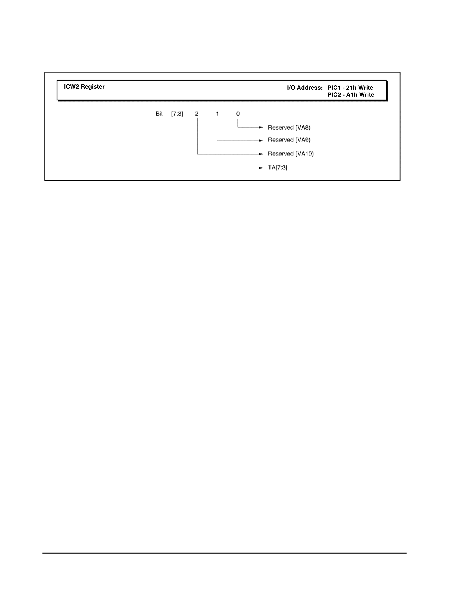
W83C553F Electrical Specifications
WINBOND SYSTEMS LABORATORY
97
Initialization Command Word 2 Register
Function: The Initialization Command Word 2 (ICW2) Register is used to initialize the interrupt controller with the
five most significant bits of the interrupt vector address. The value programmed into bits [7:3] is used by
the host CPU to define the base address in the interrupt vector table for the interrupt routines associated
with each IRQ on the controller.
Type: Write Only
Bit Description:
Bits [7:3]: TA[7:3]. Interrupt Vector Base Address. These bits define the base address in the interrupt
vector table for the interrupt routines associated with each interrupt request level input. For
Interrupt Controller #1, a typical value is "00001;" for Interrupt Controller #2, a typical value is
"10000."
Bits [2:0]: Reserved. Interrupt Request Level. When writing ICW2, these bits should all be "0." During
an interrupt acknowledge cycle, these bits are coded with a simple binary value determining
which IRQ is enable.
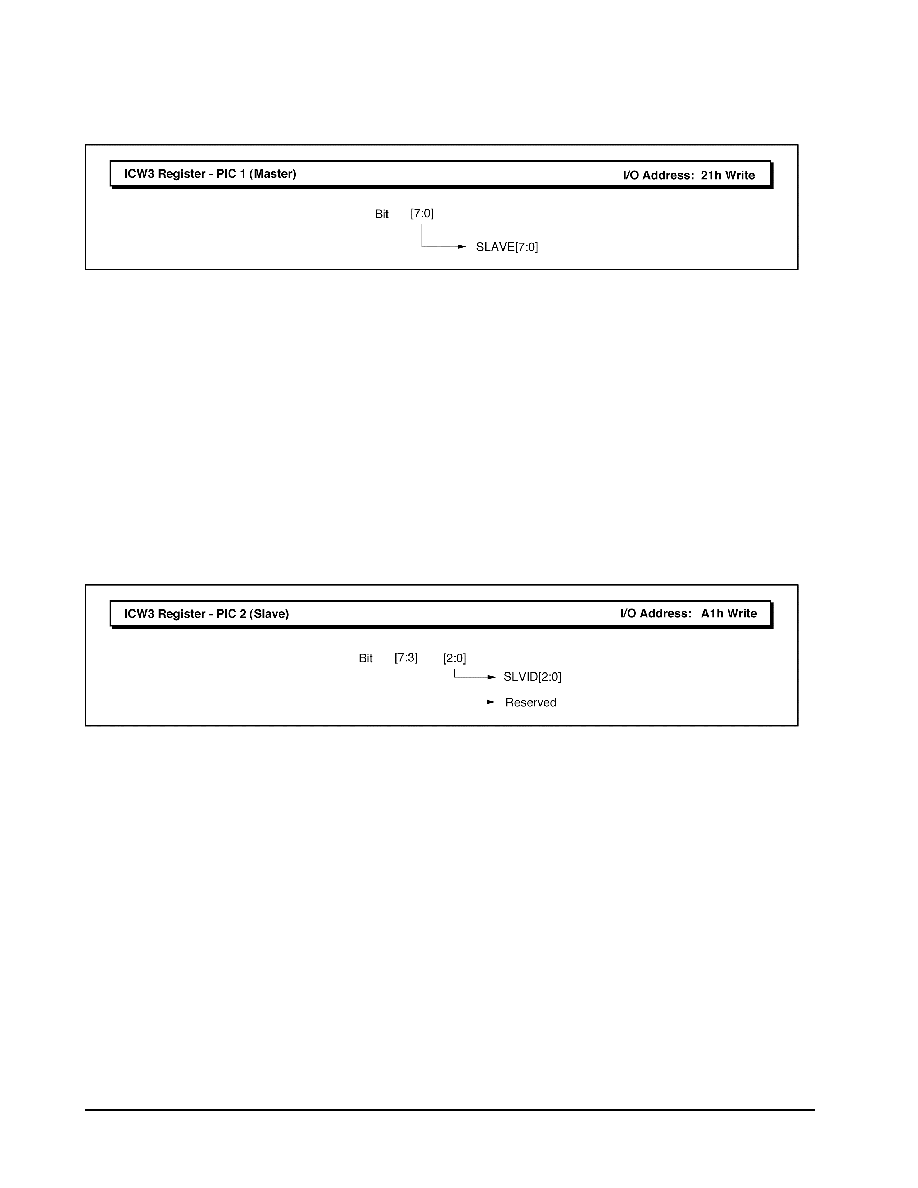
W83C553F Electrical Specifications
WINBOND SYSTEMS LABORATORY
98
Initialization Command Word 3 Register - PIC 1 (Master, default = 04h)
Function: On the Interrupt Controller #1 (the master controller), this register indicates which IRQ line physically
connects the INT output of Interrupt Controller #2 (PIC 2) to Interrupt Controller #1 (PIC 1).
Type: Write Only
Bit Description:
Bits [7:3]: SLAVE[7:3]. These bits must be programmed to "00000."
Bit 2: SLAVE2. Cascaded Interrupt Controller IRQ Connection. This bit must always be programmed
to "1." It indicates the slave controller (#2) is cascaded on IRQ2.
Bits [1:0]: SLAVE[1:0]. These bits must be programmed to "00."
Initialization Command Word 3 Register - PIC 2 (Slave)
Function: On the Interrupt Controller #2 (the slave controller), this register contains the slave identification code
broadcast by Interrupt Controller #1 from the trailing edge of the first INTA# pulse to the trailing edge of
the second INTA# pulse. It must be programmed to 02h for Interrupt Controller #2.
Type: Write Only
Bit Description:
Bits [7:3]: Reserved. These bits must be programmed to "00000."
Bits [2:0]: SLVID[2:0]. Slave Identification Code. During the initialization sequence, bits 2 and 0 must be
programmed to "0" and bit 1 programmed to a "1."
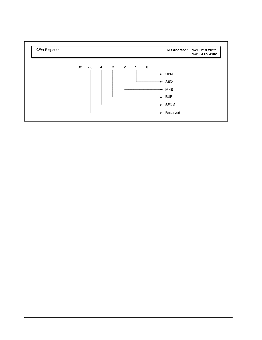
W83C553F Electrical Specifications
WINBOND SYSTEMS LABORATORY
99
Initialization Command Word 4 Register
Function: Both interrupt controllers must have the Initialization Command Word 4 (ICW4) Register programmed
as part of their initialization sequence. At a minimum, bit 0 must be set to "1" to indicate it is operating
in an x86-based system.
Type: Write Only
Bit Description:
Bits [7:5]: Reserved. These bits must be programmed to "000."
Bit 4: SFNM. Special Fully Nested Mode. This mode should normally be disabled by writing "0" to
this bit.
Bit 3: BUF. Buffered Mode. This bit must be programmed to "0" for the W83C553F.
Bit 2: MNS. Master/Slave in Buffered Mode. This bit must be programmed to "0" for the W83C553F.
Bit 1: AEOI. Automatic End of Interrupt. This bit should normally be programmed to "0." If
programmed to "1," Automatic End of Interrupt Mode is enabled.
Bit 0: UPM. Microprocessor Mode. This bit must be set to "1" to indicate the interrupt controller is
operating in an x86-based system.

W83C553F Electrical Specifications
WINBOND SYSTEMS LABORATORY
100
Operational Control Word 1 Register
Function: The Operational Control Word 1 (OCW1) Register sets and clears the mask bits in the Interrupt Mask
(IMR) Register. Each interrupt request line may be selectively masked or unmasked any time after
initialization.
Type: Read/Write
Bit Description:
Bits [7:0]: IMR[7:0]. When a "1" is written to any bit in this register, the corresponding IRQx line is
masked. When a "0" is written to any bit in this register, the corresponding IRQx mask bit is
cleared and interrupt requests will again be accepted by the controller.
Note: Masking IRQ2 on 21h will also mask interrupt requests from A1h, which is physically
cascaded to IRQ2.
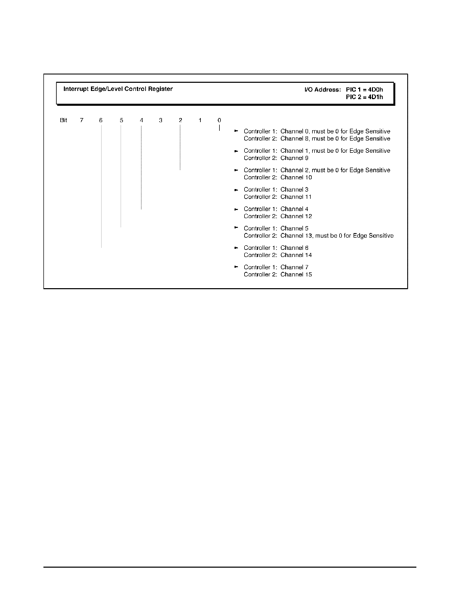
W83C553F Electrical Specifications
WINBOND SYSTEMS LABORATORY
101
Interrupt Edge/Level Control Register (default = 00h)
Type: Read/Write
Bit Description:
Bit 7: Controller 1-Channel 7. Controller 2-Channel 15.
Bit 6: Controller 1-Channel 6. Controller 2-Channel 14.
Bit 5: Controller 1-Channel 5. Controller 2-Channel 13; must be "0" for edge.
Bit 4: Controller 1-Channel 4. Controller 2-Channel 12.
Bit 3: Controller 1-Channel 3. Controller 2-Channel 11.
Bit 2: Controller 1-Channel 2; must be "0" for edge. Controller 2-Channel 10.
Bit 1: Controller 1-Channel 1; must be "0" for edge. Controller 2-Channel 9.
Bit 0: Controller 1-Channel 0; must be "0" for edge. Controller 2-Channel 8; must be "0" for edge.
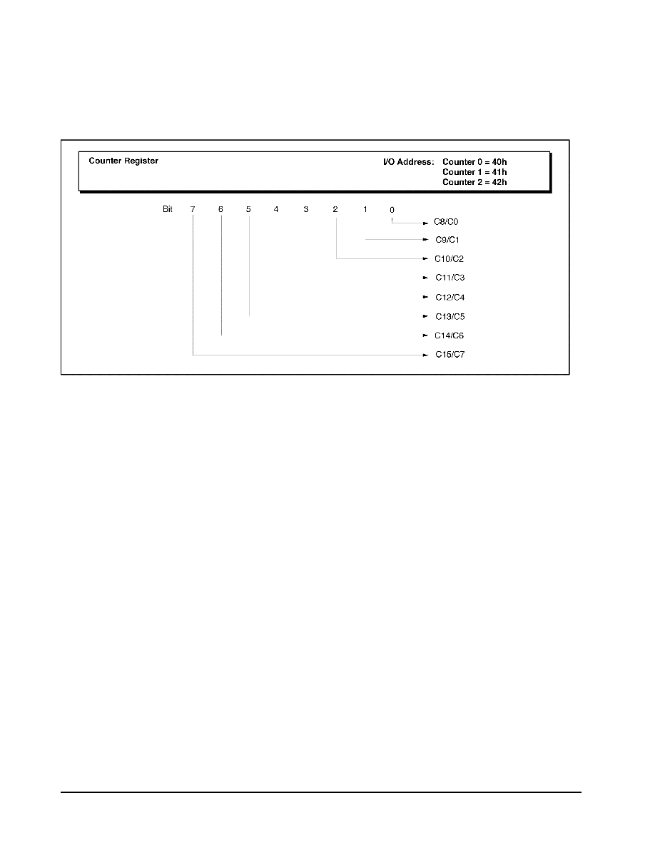
W83C553F Electrical Specifications
WINBOND SYSTEMS LABORATORY
102
4.2.3 Counter/Timer I/O Registers
Counter Register
Function: These three registers contain the actual counter values programmed into counters 0 through 2. The set
values are determined by selections made in the Timer Control Register (43h).
Type: Read/Write
Bit Description:
Bits [7:0] C[15:8]/C[7:0]. Upper and lower counter values.
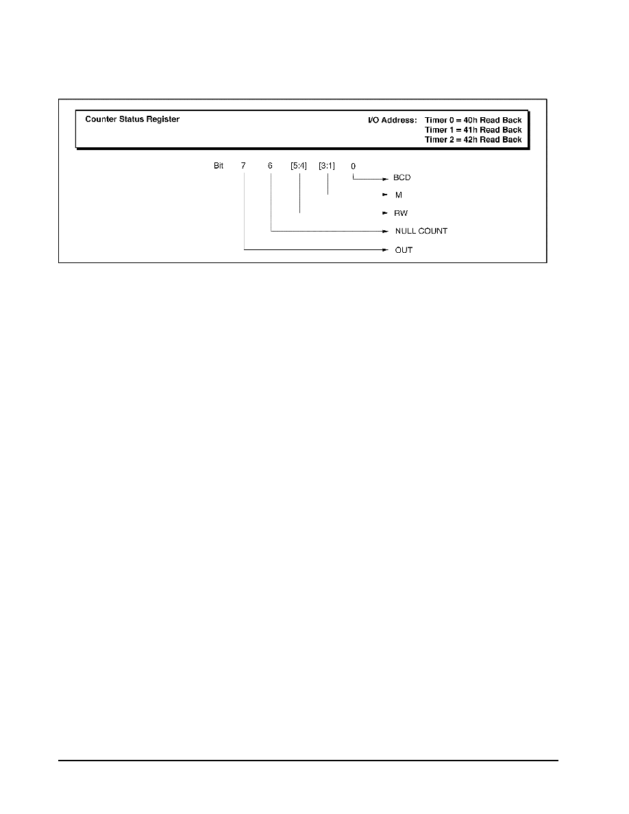
W83C553F Electrical Specifications
WINBOND SYSTEMS LABORATORY
103
Counter Status Register
Function: Each counter's status byte can be read following a timer Read Back command, as programmed in the
Timer Control Register (43h).
Type: Read back
Bit Description:
Bit 7: OUT. Count Out Status. This bit indicates the Counter Out pin state. When set to "1", the
OUT pin of the counter is also a "1". When set to "0", the OUT pin of the counter is also a "0".
Bit 6: NULLCOUNT.
Bits [5:4]: R/W. Read/Write Selection Status. These bits reflect the read/write selection made through
bits [5:4] of the control register. The binary codes returned, during the status read, match the
codes used to program the counter read/write selection.
Bit 5 Bit 4 Function
0 0 Counter Latch command
0 1 R/W Least Significant Byte (LSB)
1 0 R/W Most Significant Byte (MSB)
1 1 R/W LSB then MSB
Bits [3:1]: M. The Mode Selection Status bits return the counter mode programming. The binary code
returned matches the code used to program the counter mode, as listed under the bit function
above.
Bit 3 Bit 2 Bit 1 Mode
0 0 0 0
0 0 1 1
x 1 0 2
x 1 1 3
1 0 0 4
1 0 1 5
Bit 0: BCD. The countdown method is binary when this bit is "0", and Binary Coded Decimal (BCD)
when this bit is "1".
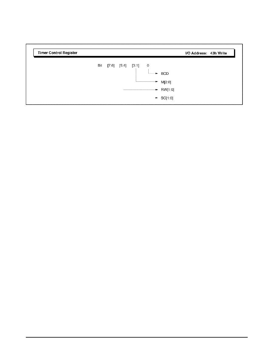
W83C553F Electrical Specifications
WINBOND SYSTEMS LABORATORY
104
Timer Control Register
Function: The Timer Control Register specifies the counter selection, operating mode, counter byte programming
order and count value size, and whether the counter counts down in a 16-bit or Binary Coded Decimal
(BCD) format. After writing the control word, a new count can be written at any time. The new value
will take effect according to the programmed mode.
Type: Write Only
Bit Description:
Bits [7:6]: SC[1:0]. These bits select the counter the control word acts upon as shown below.
Bit 7 Bit 6 Function
0 0 Counter 0 select
0 1 Counter 1 select
1 0 Counter 2 select
1 1 Read Back command
Bits [5:4]: RW[1:0]. These bits are the read/write control bits. Actual counter programming is done
through the counter I/O port (40h, 41h, 42h for counters 0, 1 and 2, respectively).
Bit 5 Bit 4 Function
0 0 Counter Latch command
0 1 R/W Least Significant Byte (LSB)
1 0 R/W Most Significant Byte (MSB)
1 1 R/W LSB then MSB
Bits [3:1]: M[2:0]. These bits select one of six possible modes of operation for the counter as shown
below.
Bit 3 Bit 2 Bit 1 Mode Function
0 0 0 0 Out signal on end of count (=0)
0 0 1 1 Hardware retriggerable one shot
x 1 0 2 Rate generator (divide by n counter)
x 1 1 3 Square wave output
1 0 0 4 Software triggered strobe
1 0 1 5 Hardware triggered strobe
Bit 0: BCD. When this bit is "0", a binary countdown is used. The largest possible binary count is
216. When this bit is "1", a Binary Coded Decimal (BCD) count is used. The largest BCD
count allowed is 104.

W83C553F Electrical Specifications
WINBOND SYSTEMS LABORATORY
105
BIOS Timer Register (default = 00000000h)
Function: After a counter value is written into the lower 16 bits of this register, it will decrement to 0 with every
BCLK.
Type: Default
Bit Description:
Bits [31:16]: Reserved.
Bits [15:0]: BTMR. BIOS Timer. When a counter in written into this field, the counter will be decremented
by 1 every BCLK until 0 is reached.
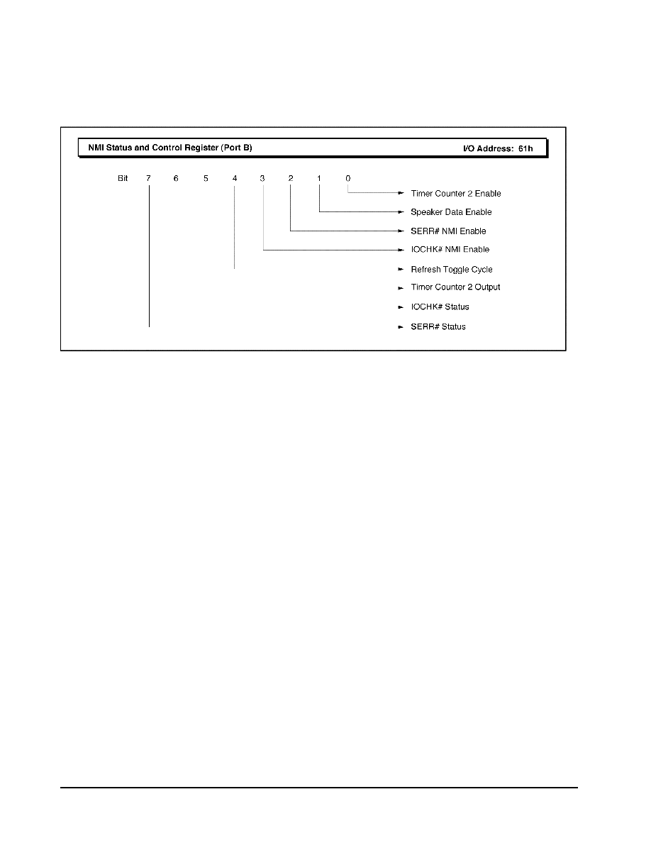
W83C553F Electrical Specifications
WINBOND SYSTEMS LABORATORY
106
4.2.4 Miscellaneous I/O Control Registers
NMI Status and Control (Port B) Register (default = 00h)
Type: Read/Write
Bit Description:
Bit 7: SERR# Status.
Bit 6: IOCHK# Status.
Bit 5: Timer Counter 2 Output.
Bit 4: Refresh Cycle Toggle.
Bit 3: IOCHK# NMI Enable.
Bit 2: SERR# NMI Enable.
Bit 1: Speaker Data Enable.
Bit 0: Timer Counter 2 Enable.
Note: for Bit 3 and Bit 2, 1= Enable; 0 = Disable.

W83C553F Electrical Specifications
WINBOND SYSTEMS LABORATORY
107
NMI Enable and RTC Address Register (default = 0xxx, xxxx)
Type: Shadow
Bit Description:
Bit 7: NMI Enable.
Bits [6:0]: RTC Address.
Share

W83C553F Electrical Specifications
WINBOND SYSTEMS LABORATORY
108
Port 92 Register (default = 24h)
Type: Read/Write
Bit Description:
Bits [7:3]: Reserved. These bits default to "00100."
Bit 2: Read only. Value of pin 116 after reset. See page 25.
Bit 1: Alt A20.
Bit 0: Hot Reset. Changing this bit from a 0 to 1 will cause a system soft reset to occur. This bit must
be returned to 0 before another soft reset can be issued.
Co-processor Error Register
Type: Write only
Bit Description:
Bits [7:0]: Co-processor Error. This register only exists in x86 mode.
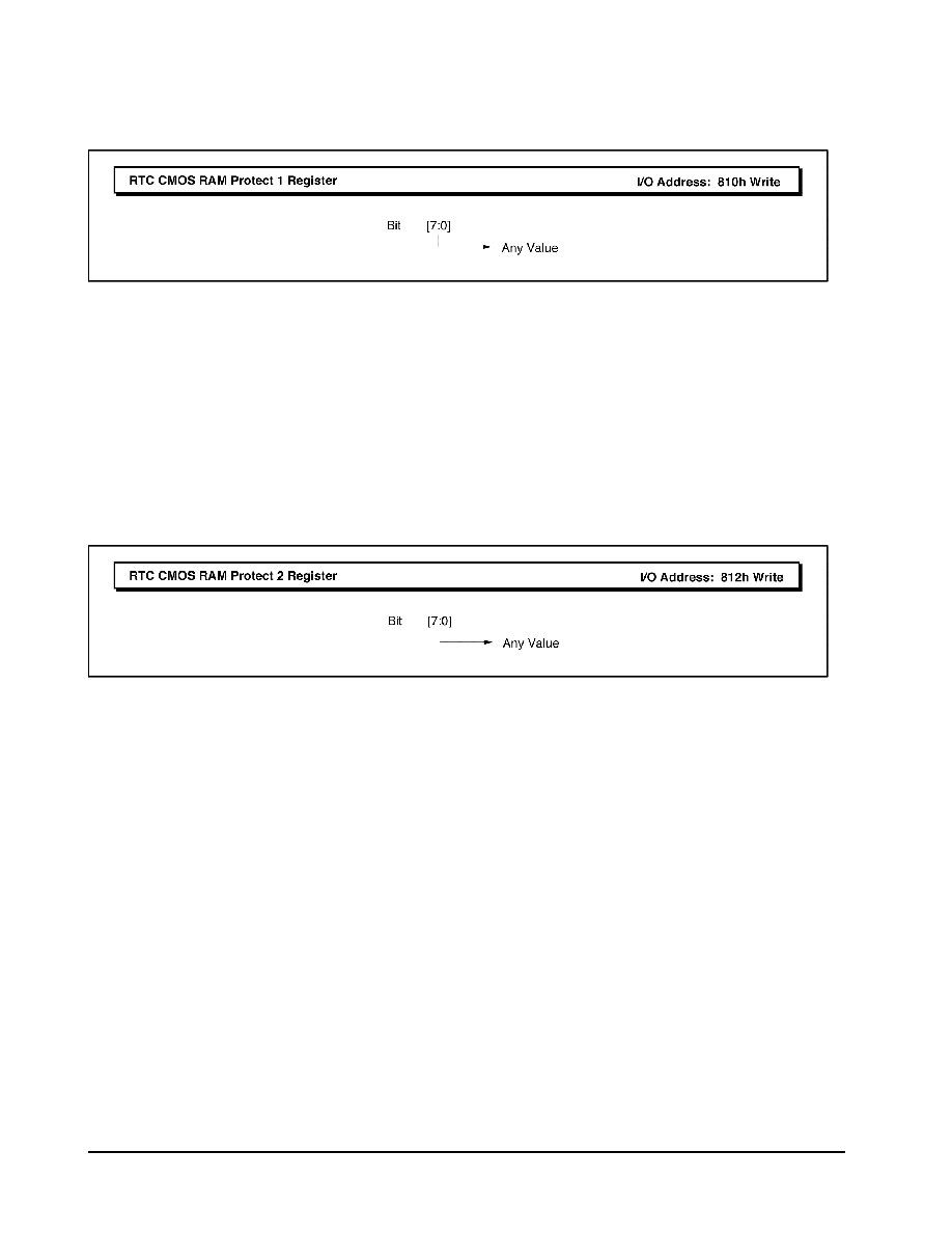
W83C553F Electrical Specifications
WINBOND SYSTEMS LABORATORY
109
RTC CMOS RAM Protect 1 Register
Type: Write only
Bit Description:
Bits [7:0]: Any value. Writing any value to this port sets a flip-flop which prevents any subsequent access
to addresses 20h - 2Fh of the Real Time Clock address space. This flip-flop is cleared only on
power-on reset. A read has no effect. This register's initial state after reset is in unprotected
mode. This register only exists in PowerPC mode.
RTC CMOS RAM Protect 2 Register
Type: Write only
Bit Description:
Bits [7:0]: Any value. Writing any value to this port sets a flip-flop which prevents any subsequent access
to addresses 30h - 3Fh of the Real Time Clock address space. This flip-flop is cleared only on
power-on reset. A read has no effect. This register's initial state after reset is in unprotected
mode. This register only exists in PowerPC mode.

W83C553F Electrical Specifications
WINBOND SYSTEMS LABORATORY
110
4.3 PCI Configuration Space - Bus Master IDE Registers (Function 1)
The configuration space is organized as 64 double word (32-bit) registers. It is divided into two sections, the PCI specified
and defined Header registers and the Control registers. Header registers are located in the first 16 double words. Control
registers are located in the last 48 double words.
Table 4-1. Bus Master IDE Configuration Space Header Registers
Address
Register Bits
31 24
23 16
15 8
7 0
03h-00h
Device ID (0105h)
Vendor ID (10ADh)
07h-04h
Device Status
Device Control
0Bh-08h
Base Class
(01h)
Sub-Class
(01h)
Programming
Interface
Revision ID
(05h)
0Fh-OCh
Reserved
(00h)
Header Type
(80h)
Latency Timer
Cache Line Size
13h-10h
Base Address 0; Port 0 Primary Registers (IDE_CS0#)
17h-14h
Base Address 1; Port 0 Auxiliary Registers (IDE_CS1#)
1Bh-18h
Base Address 2; Port 1 Primary Registers (IDE_CS0#)
1Fh-1Ch
Base Address 3; Port 1 Auxiliary Registers (IDE_CS1#)
23h-20h
Base Address 4; Bus Master IDE Registers (for DMA mode disk drives)
3Bh-24h
Reserved (00000000h)
3Fh-3Ch
MAX_LAT
(28h)
MIN_GNT
(02h)
Interrupt Pin (01h)
Interrupt Line

W83C553F Electrical Specifications
WINBOND SYSTEMS LABORATORY
111
Table 4-2. Organization of IDE Control Registers
Address
Register Bits
31 24
23 16
15 8
7 0
43h-40h
IDE Control/Status Register
47h-44h
Port 0 Drive 0 Control Register
4Bh-48h
Port 0 Drive 1 Control Register
4Fh-4Ch
Port 1 Drive 0 Control Register
53h-50h
Port 1 Drive 1 Control Register
7Bh-54h
Reserved (00000000h)
7Fh-7Ch
Reserved
FFh-80h
Reserved (00000000h)
All reserved bits and bytes return a logic 0 when read. All reserved bytes written will execute normal PCI cycles, but will not
affect the operation or device registers.
Internal register information for the W83C553F SIO is organized as follows:
� Register name and Index value offset from base address.
� Function of the signal.
� Type (Read and/or Write).
� Bit description.
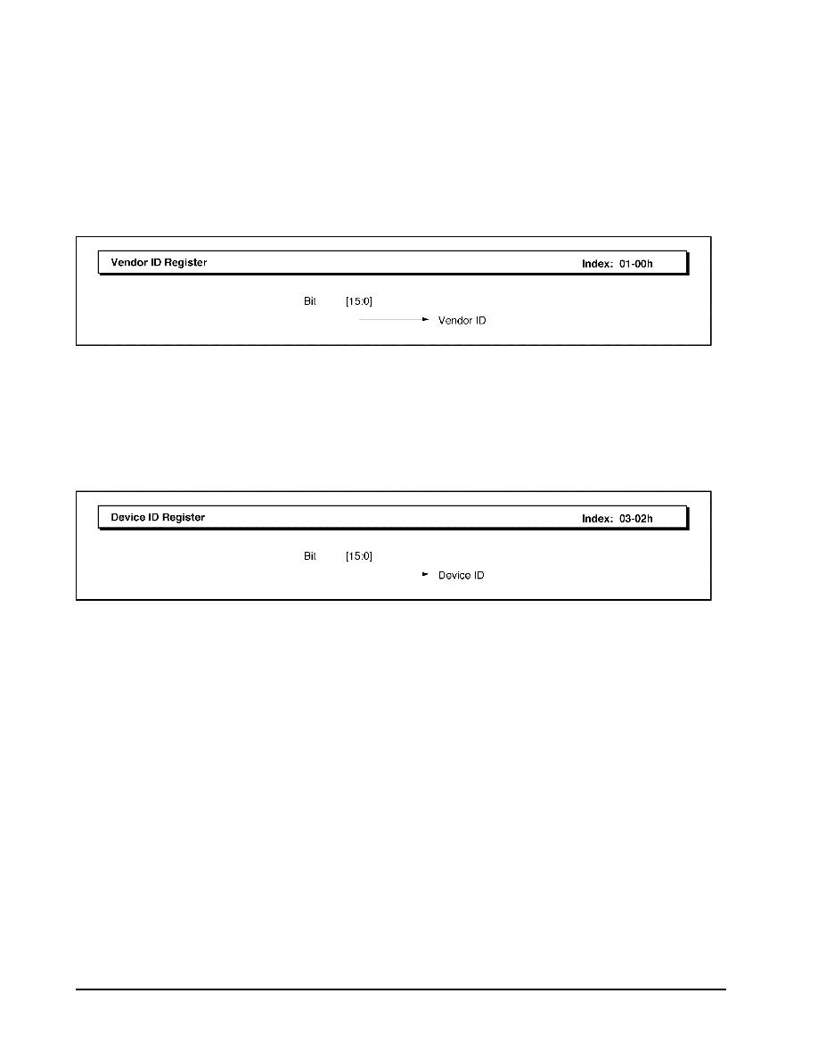
W83C553F Electrical Specifications
WINBOND SYSTEMS LABORATORY
112
4.3.1 Function 1 Header Registers
The registers contained in this address space are defined and required by the PCI Specification Revision 2.1. Six fields in the
pre-defined header deal with device identification. These fields are Vendor ID, Device ID, Revision ID, Header Type, Class
Code, and Programming Interface and their addresses are 00h-03h,08h-0Bh.
Vendor ID Register
Function: This field, containing the Vendor ID value 10ADh, identifies Symphony Labs as the manufacturer of the
device. This register is read only.
Type: Read only
Device ID Register
Function: This field, the Device ID, will identify the Bus Master IDE device with a value of 0105h (similar to the
W83789F 'Sonata' chip).
Type: Read only
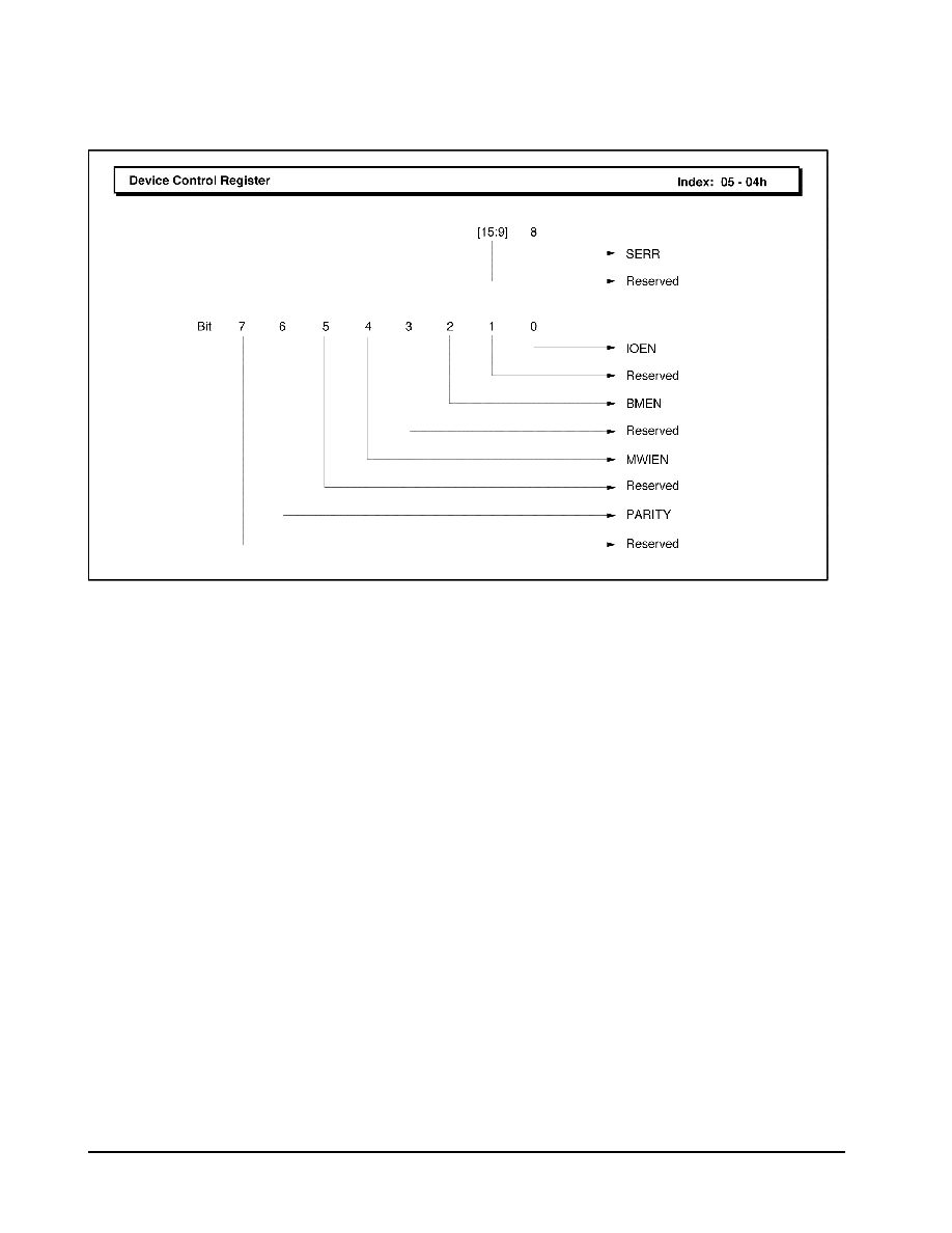
W83C553F Electrical Specifications
WINBOND SYSTEMS LABORATORY
113
Device Control Register (default = 0000h)
Function: The Device Control Register provides coarse control over the device's ability to generate and respond to
I/O cycles. Since the default value disables the IO decode, it must be programmed by the BIOS/Firmware
to enable this function.
Type: Read/Write
Bit Description:
Bit [15:9]: These bits are reserved and hardwired to a logic 0b.
Bit 8: SERR. When this bit is 1b, the SERR# output driver is enabled. A system error will only be
reported for address parity errors. Bit 6 PARITY must also be enabled, or no error will be
reported. Bit 8 is a 0b after a reset.
Bit 7: This bit is not used and is hardwired to a logic 0b.
Bit 6: PARITY. This is the enable bit for the PERR# output driver. When bit 6 is a 1b, slave write data
parity errors, and master memory read data parity errors, will be reported on PERR#. Write
data parity errors are only reported for bus cycles claimed by the W83C553F (DEVSEL#
asserted). Bit 6 is a 0b after a reset.
Bit 5: This bit is not used and is hardwired to a logic 0b.

W83C553F Electrical Specifications
WINBOND SYSTEMS LABORATORY
114
Bit 4: MWIEN. When this bit is 1b, Memory write and invalidate commands are enabled, when acting
as a bus master. When this bit is 0b, only memory writes can be used. This bit is a 0b after a
reset.
Bit 3: This bit is not used and is hardwired to a logic 0.
Bit 2: BMEN. This bit must be set to allow the W83C553F to perform bus master cycles. Writing a 1b
to this bit will set it. Also, writing a 1b to bit 0 (Start/Stop Bus Master) of the Primary or
Secondary Bus Master IDE Command Register will set this bit. This bit is a 0b after a reset.
Bit 1: This bit is not used and is hardwired to a logic 0b.
Bit 0: IOEN. When bit 0 is set to a 1b, IDE I/O address decodes, based on the W83C553F's
configuration, are enabled. Primary and/or secondary port I/O addresses are decoded if they
are also enabled in the IDE Control/Status Register. They will be the default address range,
unless the Base Address Registers are enabled and programmed. In this case, the Base
Address Registers determine the addresses to be decoded.
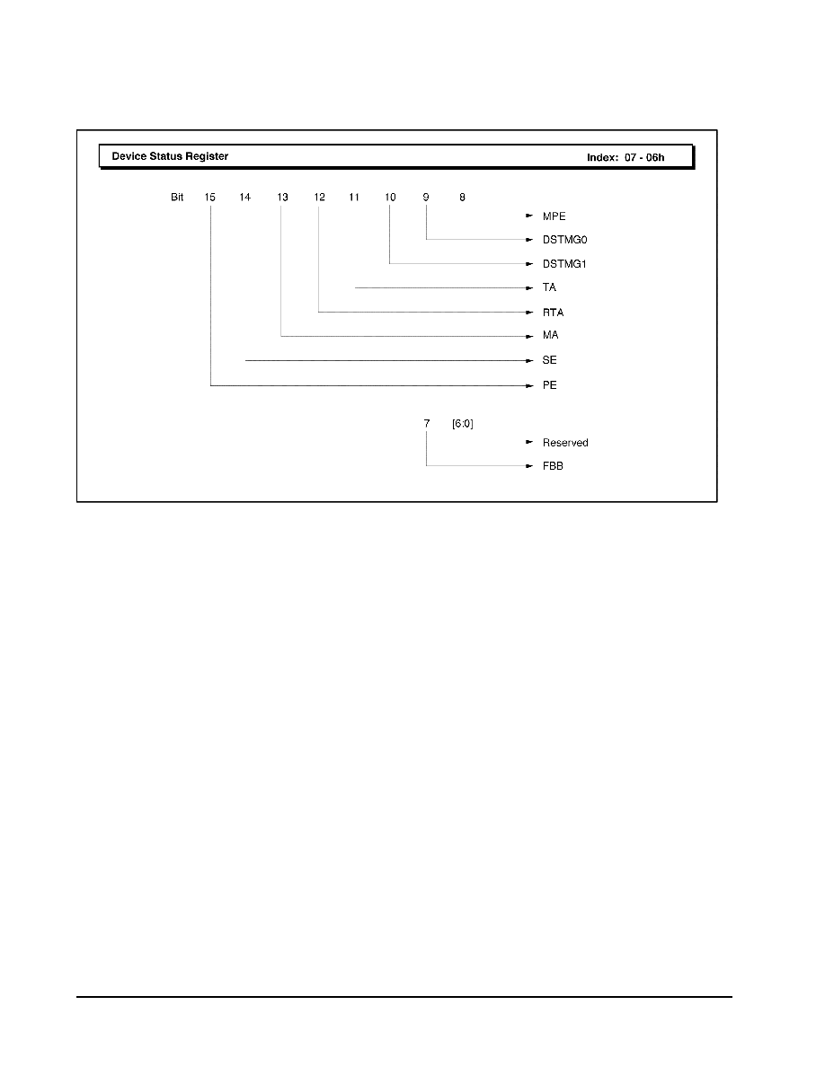
W83C553F Electrical Specifications
WINBOND SYSTEMS LABORATORY
115
Device Status Register (default = 0280h)
Function: The Device Status Register is used to record status information for PCI bus related events. Reads to this
register behave normally. Writes report slightly different, in that bits can be reset, but not set. A bit is reset
whenever the register is written, and the data in the corresponding bit is a 1b. In the cases of PE, SE, MA,
RTA, TA, or MPE been set, the software should write a "1" in the corresponding bit position to clear it,
after recovering from the error.
Type: Read/Write
Bit Description:
Bit 15: PE. This bit is set anytime a parity error is detected during a slave data write to the W83C553F,
for any command phase parity error, or when operating as a bus master for any memory read
parity error. The function of this bit is not affected by the Device Control Register parity bit.
Bit 14: SE. This bit is set anytime the W83C553F asserts the SERR# output low.
Bit 13: MA. This bit will be set when operating as a bus master and a (memory) cycle is terminated
with master abort.
Bit 12: RTA. This bit will be set when operating as a bus master and a (memory) cycle is terminated
with target abort.
Bit 11: TA. The target abort bit will be set anytime the W83C553F terminates a slave cycle with a
target abort cycle.

W83C553F Electrical Specifications
WINBOND SYSTEMS LABORATORY
116
Bit [10:9] DSTMG. These bits encode the timing of DEVSEL#. They are hardwired to 01b indicating the
support of medium DEVSEL# timing. This allows for support of fast back-to-back PCI bus
cycles. This will maximize the PCI bus bandwidth for PIO data transfer cycles.
Bit 8: MPE. This bit will be set when operating as a bus master and either the PERR# output is
driven low by the W83C553F or the target asserts PERR# and bit 6 of the Device Control
Register is set.
Bit 7: FBB. This bit will always be set. The W83C553F fully supports fast back to back transactions
to different targets.
Bit [6:0]: These bits are reserved and are hardwired to logic 0b.

W83C553F Electrical Specifications
WINBOND SYSTEMS LABORATORY
117
Revision ID Register (default = 05h)
Function: This register specifies a device specific revision identifier. The first Symphony bus master device was 01h
with subsequent bus master IDE chips being 02h, 03h, etc. This specification is written to define device
revision 05h.
Type: Read only
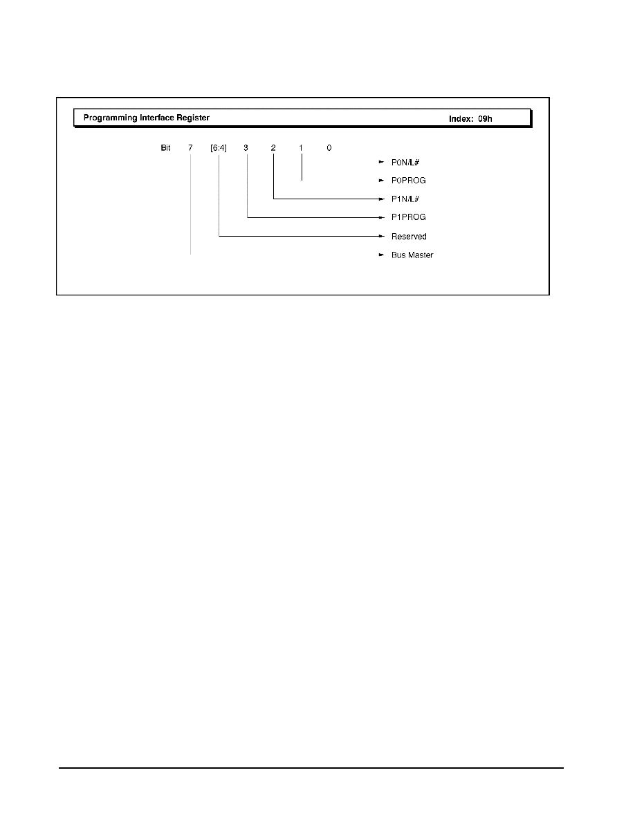
W83C553F Electrical Specifications
WINBOND SYSTEMS LABORATORY
118
Programming Interface Register ( Default = 8Ah)
Function: There are no PCI predefined configuration register sets released for this class of device but the PCI SIG has
generated two proposed interfaces which are both supported. The first interface defines native and legacy
IDE devices and is described in PCI Rev. 2.1 spec. The Programming Interface register will support both
the native and legacy modes. Also the PCI SIG group has proposed a programming interface for Bus
Master IDE controllers. This register set and protocol is fully supported as indicated by bit 7 of this register
being set.
Type: Read/Write
Bit Description:
Bit 7: Bus Master. This bit is hardwired to logic 1 to indicate support of the IDE BUS MASTER
register set and protocol.
Bit [6:4]: These bits are reserved and hardwired to logic 0.
Bit 3: P1PROG. Port 1 Programmable is hardwired to a 1b. This indicates that bit 2 of this register is
R/W.
Bit 2: If this bit is 1b, indicating in native mode, base address register (2 and 3) can be programmed.
If it is 0b, indicating legacy mode, they can not be programmed and default address will be
used.
Bit 1: P0PROG. Port 0 Programmable is hardwired to a 1b. This indicates that bit 0 of this register is
R/W.
Bit 0: If this bit is 1b, indicating in native mode, base address register (0 and 1) can be programmed.
If it is 0b, indicating legacy mode, they can not be programmed and default address will be
used.
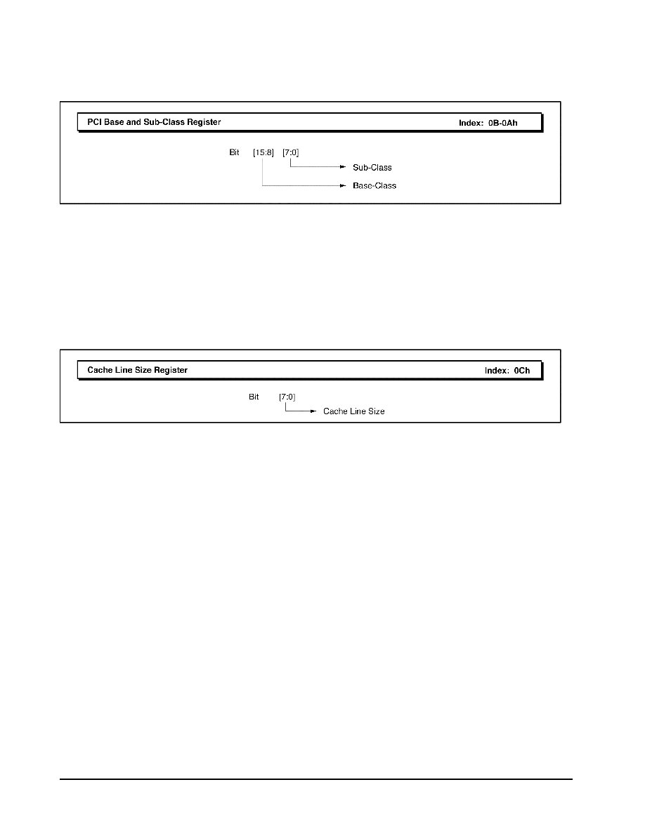
W83C553F Electrical Specifications
WINBOND SYSTEMS LABORATORY
119
PCI Base and Sub Class Register (default = 0101h)
Type: Read only
Bit Description:
Bits [15:8]: Sub Class. Permanently defaults to 01h - "IDE Controller."
Bits [7:0]: Base Class. Permanently defaults to 01h - "Mass Storage Controller."
Cache Line Size Register (default = 08h)
Function: This 8-bit register is programmed by the host to the cache line size being used by the system processor. It is
programmed in units of 32-bit double words. The programmed value effects the memory read and write
commands executed when the W83C553F is operating as a bus master. The default value is 08h. This
register can only be programmed to 04h (16 bytes), 08h (32 bytes), or 00h (4 bytes); all other values will be
ignored.
Type: Read/Write
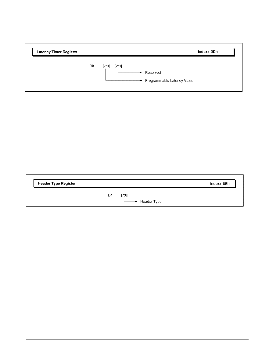
W83C553F Electrical Specifications
WINBOND SYSTEMS LABORATORY
120
Latency Timer Register (default = 00h)
Function: This register specifies, in PCI bus clocks, the value of the latency timer when operating as a bus master.
Bits 0 through 2 are hardwired to a 0b. Bits 3 through 7 are programmable allowing a programmable
latency value in increments of 8 PCI clocks. The result is a timer granularity of eight clocks. This register
has a default value of 00h.
Type: Read/Write
Bit Description:
Bit [7:3] High-order Timer Bits. Five programmable timer value bits.
Bit [2:0] Low-order Timer Bits. Hardwire to ground for read-only 0b values.
Header Type Register (default = 80h)
Type: Read only
Bit Description:
Bits [7:0]: This byte identifies the layout of bytes 10h through 3Fh in the configuration space. A default
value of 80h specifies the class codes shown in Table 6-1 of the PCI Specification.

W83C553F Electrical Specifications
WINBOND SYSTEMS LABORATORY
121
Base Address Registers 0 through 3 (10h-13h, 14h-17h, 18h-1Bh, 1Ch-1Fh)
The W83C553F can be configured to support these Base Address Registers or to disable them. This can be useful in
configuring the device to operate in PCI systems that have various levels of configuration compatibility. Base Address
Registers 0 and 1 are used to control the primary IDE port I/O address locations. Base Address Registers 2 and 3 are used to
control the secondary IDE port I/O address locations. IOR[A:B]# and IOW[A:B]# are used with IDECS0# and IDECS1# to
access the primary and second ports. Note: A Base Address register does not contain a valid address when it is equal to "0".
Table 4-3. Base Address Register Mapping
Base
Address
Register
Address
Decode
IDE Chip
Select
Default When
Enabled
Value When
Programmed
FF FF FF FFh
0
1F0h-1F7h
IDE_CS0#
00 00 01 F1h
FF FF FF F9h
1
3F6h
IDE_CS1#
00 00 03 F5h
FF FF FF FDh
2
170h-177h
IDE_CS0#
00 00 01 71h
FF FF FF F9h
3
376h
IDE_CS1#
00 00 03 75h
FF FF FF FDh
When P0N/L# bit in Programming Interface Register is set, Base Address Register 0,1 can be programmed for relocation to
any address within the 32 bit PCI I/O address space.
When P1N/L# bit in Programming Interface Register is set, Base Address Register 2,3 can be programmed for relocation to
any address within the 32 bit PCI I/O address space.
The default values of all the registers are located above.
When relocating the IDE ports, the normal procedure is to first program the Base Address Register with a value of FF FF FF
FFh. Next the register is read. Base Address Registers 0 and 2 will respond with a value of FF FF FF F9h indicating a
decode range of 8 bytes in I/O space, while 1 and 3 will respond with a value of FF FF FF FDh indicating a decode range of 4
bytes in I/O space. Although Base Address Registers 1 and 3 indicate a decode of 4 bytes, they will only claim cycles to byte
lane 2 (of 0 through 3) of the 4 byte range. This means that register accesses to 3F4h, 3F5h, 3F7h, 374h, 375h or 377h (or the
equivalent offset) will not be claimed or executed.
The W83C553F will only decode IDE port addresses if the IOEN bit of the Device Control Register is high and the IDE port
is enabled in the W83C553F function 1: IDE Control/Status Registers.

W83C553F Electrical Specifications
WINBOND SYSTEMS LABORATORY
122
Base Address Register 4 (20h-23h)
This Base Address Register is used to define the I/O address of the Bus Master IDE Register set in systems which use multi-
word DMA mode disk drives. This register set is internal to the W83C553F but is located in the I/O address space instead of
the Configuration address space. The default value of Base Address Register 4 is 00000001h. When programmed with a
value of FFFFFFFFh, a value of FFFFFFF1h will be read back indicating a required address range of 16 bytes. The Bus
Master IDE Register set can be located anywhere in the 32 bit I/O address space. Since address 00 00 00 00h is the address
of the motherboard DMA controller, no cycles will be claimed until Base Address Register 4 is programmed to a non-zero
address and IOEN is set in the Device Control Register. The lower 4 bits are hardwired to a value of 1h. Note: A Base
Address register does not contain a valid address when it is equal to "0".
Interrupt Line Register (3Ch)
The Interrupt Line register is an 8-bit register used to communicate interrupt line routing information. This register is
read/write. The POST software is expected to write the appropriate routing information into this register as it initializes and
configures the system. At reset, this register is set to 0Eh to indicate the desired interrupt path to the interrupt controller is
through IRQ14.
Interrupt Pin Register (3Dh)
The Interrupt Pin register is an 8-bit register that defines which interrupt pin the device uses. A value of 01h is hardwired to
this register to signify that INTA# is being used. This interrupt may be a PCI interrupt or an ISA interrupt (i.e. IRQ14).

W83C553F Electrical Specifications
WINBOND SYSTEMS LABORATORY
123
Min. Grant (3Eh) and Max. Latency (3Fh) Registers
These read-only registers specify the desired latency timer value. They each represent a number of 1/4 microsecond time
units.
The Min Grant is the time required to complete a worst case burst assuming a 33MHz PCI clock. The hard coded value is
02h which represents 0.5�s.
The Max Latency specifies how often the W83C553F needs to gain control of the PCI bus. The hard coded value is 28h
which represents 10�s.

W83C553F Electrical Specifications
WINBOND SYSTEMS LABORATORY
124
4.3.2 Function 1 Control Registers
These configuration registers control various features of the W83C553F and the IDE interface. Reserved registers are
hardwired to a 00h and cannot be programmed. The first register controls the general features of the W83C553F and both
IDE ports. The next four registers control the features and timing of the 4 individual IDE devices. All features of the IDE
interface that have no effect on the performance of the mass storage subsystem have been set to fixed values in hardware (i.e.;
all 8-bit timing).

W83C553F Electrical Specifications
WINBOND SYSTEMS LABORATORY
125
IDE Control/Status Register
Function: This register controls the two IDE ports of the W83C553F.
Type: Read/Write

W83C553F Electrical Specifications
WINBOND SYSTEMS LABORATORY
126
Bit Description:
Bit 31: Reserved. This bit is hardwired to 0b.
Bit 30: IDE_IRQB. This is the IDE_IRQB input signal. It reflects the unbuffered state of the IDE_IRQB
input.
Bit 29: Reserved. This bit is hardwired to 0b.
Bit 28: IDE_IRQA. This is the IDE_IRQA input signal. It reflects the unbuffered state of the IDE_IRQA
input.
Bit 27: Reserved. This bit is hardwired to 0b.
Bits [26:16]: RA[10:0]. These bits control the read-ahead duration for the IDE interface. Read-ahead
duration is defined as the number of 16-bit IDE data reads that will be prefetched independent
of any PCI bus cycles. The actual read ahead count will equal the programmed value plus one
cycle. The default value is 0FFh (255 decimal + 1) for 256 16-bit IDE cycles (512 bytes).
Bits [15:12]: Reserved. These bits are hardwired to 0000b.
Bit 11: LEGIRQ. This bit and bit 2 of the Programming Interface Register control the interrupt
destination for both the IDE ports, in association with function 0 IDE_Interrupt_Routing_Control
_Register (43H) . The default value of function 0, IDE Interrupt Routing Control Register is EFh,
indicating primary port interrupt goes to IRQ 14, and secondary interrupt goes to IRQ15. When
LEGIRQ=1, for using legacy interrupts, the function 0 IDE_Interrupt_Routing Control Register
should be programmed to value 0, indicating legacy interrupt internal routing to INTC# and/or
INTD# are desired, as shown below. The default state is 0b.
LEGIRQ P1N/L# IDEIRQA IDEIRQB
0 x IRQ14 IRQ15
1 0 INTC# INTD#
1 1 INTC# INTC#
Bit [10:8]: Reserved. These bits are hardwired to 0b.
Bit 7: Reserved.
Bit 6: Reserved. This bit is hardwired to 0b.
Bit 5: P1F16. Port 1 Fast 16 controls the operation of Port 1 (secondary port) when executing 16 bit
PIO cycles on the PCI bus. When reset (0b), all 16 bit cycles to Port 1 will operate using the
default 8-bit timing (Mode 0 compatible). Also, posted writes, read ahead and IDE_IOCHRDY
will be disabled for 16-bit cycles. When set to 1b, 16-bit cycles will operate using the
programmed speed setting, while posted writes, read ahead, and IDE_IOCHRDY will be
supported as programmed in the applicable Port x Drive x Control Register. Bit 5 is cleared to
a 0b after reset or if the secondary port receives a soft reset, defined as any time the secondary
port device control register (default address 376h) is written with bit 2 a 1b.
Bit 4: P1EN. This is the secondary port enable bit. When set and IOEN is set in the Control Register,
I/O cycles to the secondary port will be claimed and executed. When 0b or IOEN is 0b, all
secondary port cycles will be ignored. The default value of this bit is "1."
Bit [3:2]: Reserved. These bits are hardwired to 0b.
Bit 1: P0F16. Port 0 Fast 16 functions the same as bit 5, but for Port 0 (Primary Port). Similarly, this
bit is cleared any time the primary port device control register (default address 3F6h) is written
with bit 2 a 1b.
Bit 0: P0EN. This is the primary port enable bit. When set and IOEN in the Control Register is
enabled, I/O cycles to the primary port will be claimed and executed. When 0b or IOEN is 0b,
all primary port cycles will be ignored. The default value of this bit is 1b.
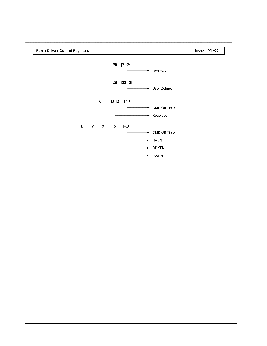
W83C553F Electrical Specifications
WINBOND SYSTEMS LABORATORY
127
Port x Drive x Control Registers
Function: These registers control the features of the four devices connected to the two ports. All four registers are
identical and control the features of only one device. The Port 0 Drive 0 Control Register (44h-47h)
controls the features of the master drive attached to the primary port. The Port 0 Drive 1 Control Register
(48h-4Bh) controls the features of the slave drive attached to the primary port. The Port 1 Drive 0 Control
Register (4Ch-4Fh) controls the features of the master drive attached to the secondary port. The Port 1
Drive 1 Control Register (50h-53h) controls the features of the slave drive attached to the secondary port.
The command timing controls only affect 16-bit and 32-bit accesses.
Calculations (refer to Table 4-4):
CMD ON TIME programmed value = (DIOR#/DIOW# 16-bit min+29) / 30ns clock - 1, after
removing all digits to the right of the decimal point (see Table 4-4).
CMD OFF TIME programmed value = ((Cycle Time minimum � (CMD ON TIME programmed value
+ 1) * 30ns + 29)) / 30ns clock -1, after removing all digits to the right of the decimal point (see Table
4-4).
CMD ON TIME = Bits [12:8] of Port x Control x Registers , which are the registers of Configuration
Space 44h-54h.
CMD OFF TIME = Bits [4:0] of Port x Control x Registers , which are the registers of Configuration
Space 44h-54h.

W83C553F Electrical Specifications
WINBOND SYSTEMS LABORATORY
128
Type: Read/Write
Bit Description:
Bits [31:24]: Reserved. These bits are hardwired to a 0b.
Bits [23:16]: User Defined. These bits are read/write and do not affect the operation of the W83C553F.
They can be used by the driver as a temporary storage. These bits will be 0b after reset.
Bits [15:13]: Reserved. These bits are hardwired to a 0b.
Bits [12:8]: CMD ON TIME. The value programmed to these bits controls the IDE_IOR# and IDE_IOW#
"ON" (low) time in clock cycles for this device. The actual number of clocks is the value
programmed plus one clock. The default value is 9h or 10 clocks. This value affects both PIO
and DMA timing.
Bit 7: PWEN. Posted write enable must be set to execute posted writes for this device. When this bit
is a 1b, posted writes are enabled. When this bit is a 0b, the default state, posted writes are
disabled.
Bit 6: RDYEN. When set, the IDE_IOCHRDY signal from the IDE interface is enabled and can insert
wait states when this device is accessed. When 0, the IDE_IOCHRDY signal will have no effect
on accesses to this device. This bit will be 0b after a reset.
Bit 5: RAEN. Read-ahead enable must be enabled to execute read-ahead for this device. When this
bit is a 1b, read-ahead is enabled. When this bit is a 0b, the default state, read-ahead is
disabled.
Bits [4:0]: CMD OFF TIME. The value programmed to these bits controls the IDE_IOR# and IDE_IOW#
"OFF" (high) time in clock cycles for this device. The actual number of clocks is the value
programmed plus one clock. The default value is 9h or 10 clocks. This value affects both PIO
and DMA timing.

W83C553F Electrical Specifications
WINBOND SYSTEMS LABORATORY
129
Table 4-4. Programming CMD ON and CMD OFF Times
(for 33 MHz PCI Bus Clock)
Drive Operation
Mode
Cycle Time /
DIOR#/DIOW# 16-bit
(minimum)
CMD ON TIME Clocks
(Programmed/Actual)
CMD OFF TIME Clocks
(Programmed/Actual)
PIO Mode 0
600ns/165ns
5/6
13/14
PIO Mode 1
383ns/125ns
4/5
7/8
PIO Mode 2
240ns/100ns
3/4
4/5
PIO Mode 3
180ns/80ns
2/3
2/3
PIO Mode 4
120ns/70ns
2/3
0/1
PIO Mode 5
(proposed)
90ns/50ns
1/2
0/1
Single Word DMA
Mode 0
960ns/480ns
15/16
15/16
Multiword DMA
Mode 0
480ns/215ns
7/8
7/8
Multiword DMA
Mode 1
150ns/80ns
2/3
1/2
Multiword DMA
Mode 2
120ns/70ns
2/3
0/1
Multiword DMA
Mode 3
(proposed)
90ns/50ns
1/2
0/1

W83C553F Electrical Specifications
WINBOND SYSTEMS LABORATORY
130
4.4 Bus Master IDE (Function 1) I/O Registers
The Bus Master IDE Register set is defined by the PCI SIG. It is composed of 16 8-bit registers and is located at the I/O
address specified by Base Address Register 4. The registers can be accessed 8, 16, 24, or 32 bits at a time.
This register set is supplied to offer a higher performance lower overhead IDE disk protocol. With this protocol, the host
(PCI) transfers will be bus master cycles and the IDE device transfers will be DMA. The normal PIO protocol uses I/O
transfers on both the host and IDE interfaces. Primary and Secondary refer to the primary and secondary IDE ports. Both
register sets are identical.
Table 4-5. Bus Master IDE I/O Register Organization
Offset from
Register Bits
Base Address
31 24
23 16
15 8
7 0
03h - 00h
Reserved
Primary Status
Register
Reserved
Primary Command
Register
07h - 04h
Primary PRD Table Address
0Bh - 08h
Reserved
Secondary Status
Register
Reserved
Secondary Command
Register
0Fh - 0Ch
Secondary PRD Table Address
Note: The registers shown in Table 4-5 cannot be accessed until after Base Address Register 4 is written (with any non zero
value).
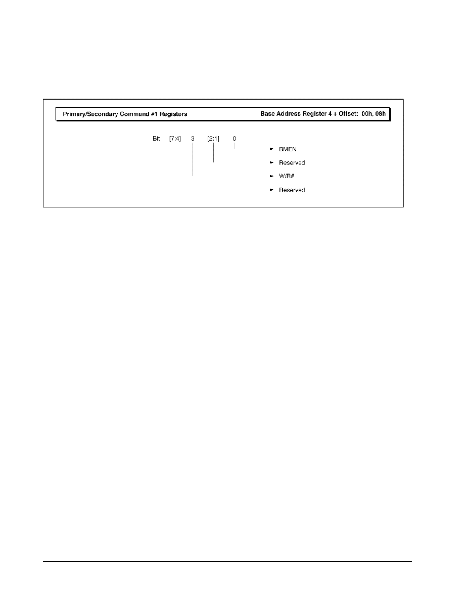
W83C553F Electrical Specifications
WINBOND SYSTEMS LABORATORY
131
4.4.1 Primary/Secondary Command Registers
Primary/Secondary Command #1 Registers
Function: These registers are used to control DMA data transfers to/from the two IDE ports when multi-word DMA
disk drives are used.
Type: Read/Write
Bit Description:
Bits [7:4]: These bits are hardwired to 0b.
Bit 3: W/R#. This bit controls the bus master transfer direction. Low is PCI memory to IDE device and
high is IDE device to PCI memory. This bit must not be changed while the bus master function
is active as defined by bit 0.
Bits [2:1]: These bits are hardwired to 0b.
Bit 0: BMEN. Bus Master operation is active when this bit is set. The bus master operation can be
terminated by writing a 0b to this bit but is considered as an abort and can not be resumed.
Writing a 1b to this bit will also set the BMEN bit in the Device Control Register.
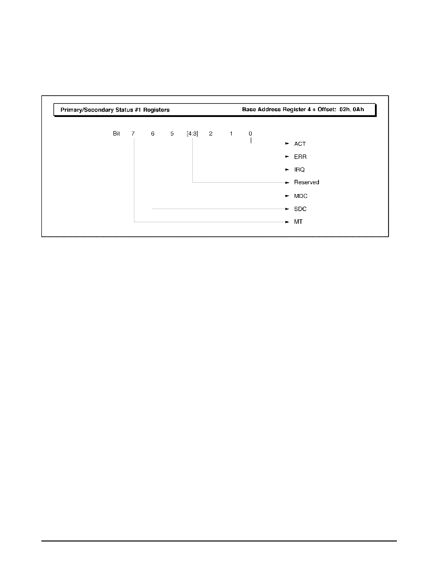
W83C553F Electrical Specifications
WINBOND SYSTEMS LABORATORY
132
4.4.2 Primary/Secondary Status Registers
Primary/Secondary Status #1 Registers (default = 00h)
Function: These register descriptions are the same and are used to control the two IDE ports under the protocol,
which requires a multi-word DMA-capable disk drive in order for the W83C553F to function as a PCI
master.
Type: Read/Write
Bit Description:
Bit 7: MT. The multithread bit is hardwired to a 0b to indicate that both channels operate
independently and can be used at the same time.
Bit 6: SDC. Slave drive DMA capable is a status bit that is set by a driver/program to indicate that the
slave drive on the indicated port is DMA capable and that the W83C553F. is initialized for
optimal performance. This bit is a 0b after a reset.
Bit 5: MDC. Master drive DMA capable is a status bit that is set by a driver/application to indicate that
the master drive on the indicated port is DMA capable and that the W83C553F. is initialized for
optimal performance. This bit is a 0b after a reset.
Bit [4:3]: These bits are hardwired to a 0b.
Bit 2: IRQ. This bit is set by the rising edge of the associated ports IDE_IRQ signal. This bit is
cleared by writing a 1b to it. On data transfers from an IDE device to system memory, this bit
will be delayed until all data has been transferred to memory. This bit is a 0b after a reset. A
noise filter has been added to the IDE_IRQ inputs.
Bit 1: ERR. This bit is set when the controller encounters an error when transferring data to/from
system memory. The specific error conditions are errors that would cause bit 8, 12, or 13 of the
Device Status register to become set. This bit is reset by writing a 1b to it. This bit is a 0b after
a reset.
Bit 0: ACT. This bit is set when the start bit of the command register is written with a 1b. It is cleared
when the start bit is written with a 0b (abort condition) or when the last transfer for a region is
performed where EOT is set in that region descriptor (normal termination).

W83C553F Electrical Specifications
WINBOND SYSTEMS LABORATORY
133
4.4.3 Primary/Secondary PRD Table
(Base Address Register 4 value + offset: 07h-04h, 0Fh-0Ch)
These registers contain the starting address of the first Physical Region Descriptor Table in memory which applies to cases
where the W83C553F is functioning as a PCI bus master with one or more multi-word DMA mode disk drives. Bits 31
through 2 define a double word aligned address in memory. Bits 1 and 0 are reserved and will be ignored on writes and read
as 00b. The information in the descriptor table controls where the data is transferred to/from in system memory, how much
data is transferred and when the transfer is complete.
The descriptor table is composed of one or more Physical Region Descriptors. Each entry is two double words (8 bytes) and
is defined below.
Table 4-6. Physical Region Descriptor
Data Bits
Dword
31 16
15 0
0
Memory Region Physical Base Address (31:2)
00
1
EOT Reserved
Byte Count
The Memory Region Physical Base Address specifies a word aligned address in memory that the bus master will transfer data
to/from.
The byte count specifies the number of bytes of data to transfer to this region of memory. The byte count is required to be
even (D0=0b). The maximum number of bytes defined in one descriptor entry is 64K which is selected by a value of 00h.
The number of bytes specified must not cause the memory region specified to cross a 64K boundary.
Bit 31 of double word 1 is the End Of Table flag. Bus master operation terminates upon completion of the descriptor entry
that has EOT set.
The Physical Region Descriptor Table cannot cross a 64K memory boundary.

W83C553F Electrical Specifications
WINBOND SYSTEMS LABORATORY
134
5.0 ELECTRICAL SPECIFICATIONS
This section contains all electrical specifications for Winbond Systems Laboratory W83C553F SIO chip. The W83C553F
must meet all absolute maximum ratings to avoid being damaged; and all combinations of the AC, DC and recommended
operating specifications.
Table 5.1. Absolute Maximum Ratings
Parameter
Values
Min Max
Notes
Storage Temperature
-40�C 125�C
Supply Voltage (Vdd)
-0.5V 7.0V
Input Voltage
-0.5V Vdd
+0.5V
Output Voltage
-0.5V Vdd
+0.5V
Table 5-2. Recommended Operating Ranges
Parameter
Values
Min Max
Notes
VDD DC Supply Voltage
4.75V 5.25V
VIN Input Voltage
VSS VDD
Operating Temperature
0 +70�C

W83C553F Electrical Specifications
WINBOND SYSTEMS LABORATORY
135
Table 5.3. DC Characteristics (Ta=0�C to 70�C, Vdd=5V+/-5%)
Parameter
Values
Min Max
Notes
Input low level
- 0.8V
TTL. 0.5V typical
Input high level
5.5V
TTL. 2.0V typical
Output low voltage:
4mA buffer, IOL=4mA
8mA buffer, IOL=8mA
12mA buffer, IOL=12mA
16mA buffer, IOL=16mA
0.4V
0.4V
0.4V
0.4V
0.15V typical
0.18V typical
0.18V typical
0.17V typical
Output high voltage:
4mA buffer, IOL=4mA
8mA buffer, IOL=8mA
12mA buffer, IOL=12mA
16mA buffer, IOL=16mA
3.0V -
3.0V -
3.0V -
3.0V -
4.54V typical
4.44V typical
4.46V typical
4.46V typical
Input low current
with 50K pullup resistor
-10uA -
-250uA -20uA
-0.01uA typical
-80uA typical
Input high current
- 10uA
0.01uA typical
Tristate output off current low
-10uA -
-0.01uA typical
Tristate output off current high
- 10uA
0.01uA typical
Input capacitance**
- -
10pF typical
Output capacitance**
- -
10pF typical
I/O capacitance**
- -
10pF typical
* Typical is under the condition of Vdd=5.0+/-5% and Ta=25 degree C.
** Capacitance includes the capacitance of I/O cell plus package pin.

W83C553F Timing Diagrams
WINBOND SYSTEMS LABORATORY
136
6.0 TIMING DIAGRAMS
This chapter lists the following PCI, ATA, and ISA timing information:
� PCI Clock Timing
� PCI Bus Timing
� IDE Interface Timing
� IDE Data Transfer Timing
� Miscellaneous Timing
� Example PIO ATA Data Transfer Timing
� Example Single Word DMA ATA Data Transfer Timing
� Example Multiword DMA ATA Data Transfer Timing
� ISA Bus Timing
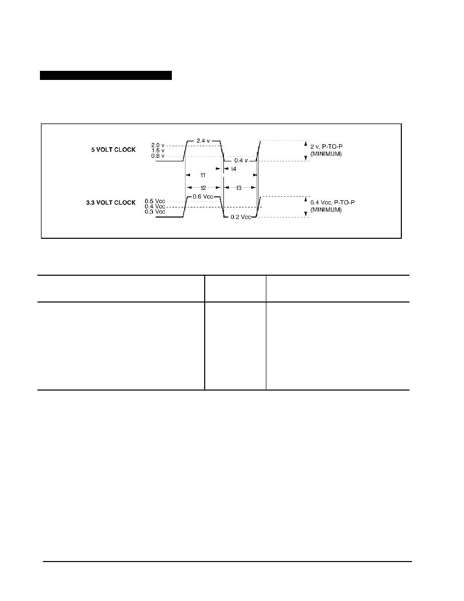
W83C553F Timing Diagrams
WINBOND SYSTEMS LABORATORY
137
6.1 PCI Timing Diagrams
This section provides timing information on PCI cycles supported by the W83C553F.
Table 6-1. PCI Clock Timing
Note: For 5V PCI Bus, measurements were taken from 0.4V to 2.4V.
All VDD are 4.75V to 5.25V
Parameter
Values
Min Max
Notes
t1 CLK cycle time
30ns
The W83C553F will operate properly at any
frequency between 0 and 33 MHz.
t2 CLK high time
11ns -
t3 CLK low time
11ns -
t4 CLK slew rate
1V/ns 4V/ns
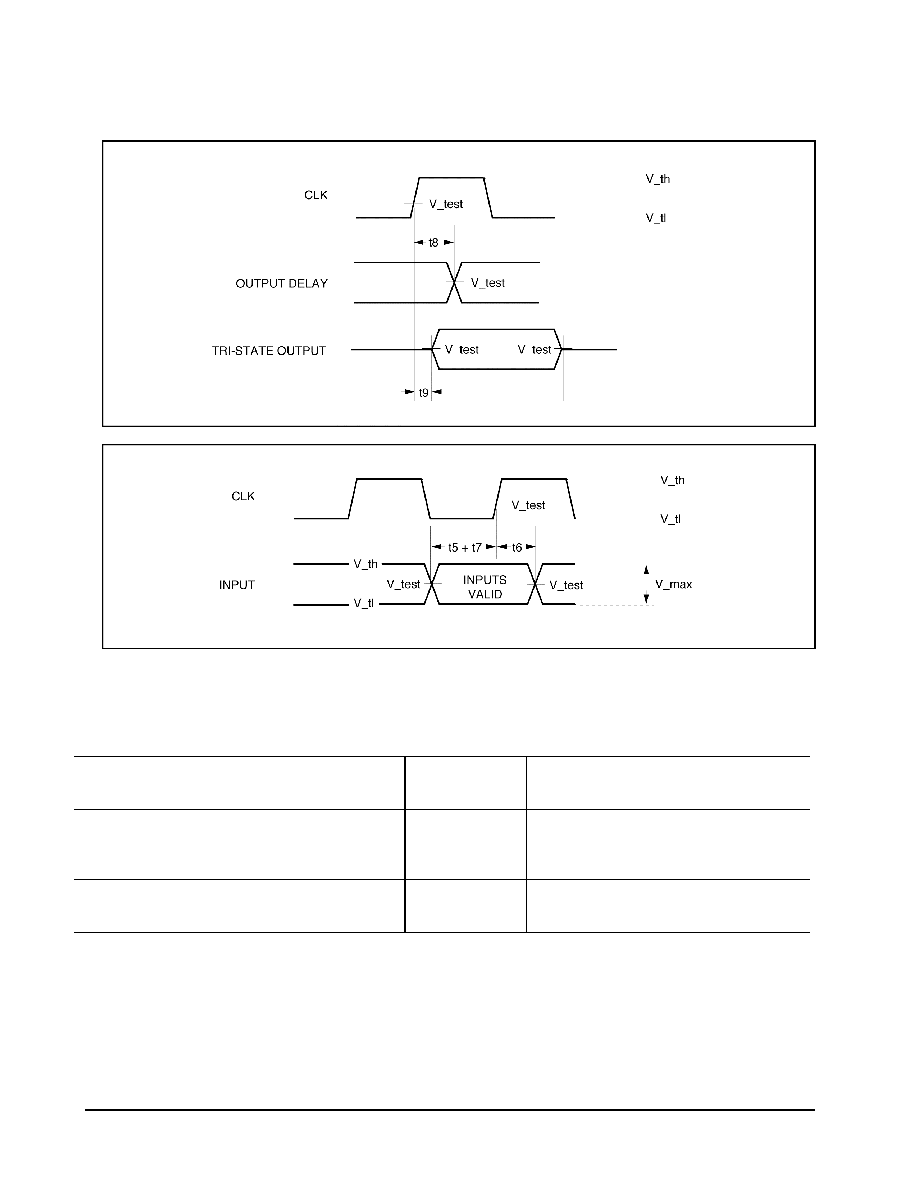
W83C553F Timing Diagrams
WINBOND SYSTEMS LABORATORY
138
Table 6-2. PCI Bus Timing
Note: For 5V PCI Bus, measurements were taken from 0.4V to 2.4V.
All VDD are 4.75V to 5.25V
Parameter
Values
Min Max
Notes
t5 Setup to CLK rising
7ns -
All PCI bussed signals, except REQ# and
GNT#.
t6 Hold from CLK rising
0ns -
All PCI bussed signals.

W83C553F Timing Diagrams
WINBOND SYSTEMS LABORATORY
139
Table 6-2 (continued). PCI Bus Timing
Parameter
Values
Min Max
Notes
t7 Setup to CLK rising
10ns -
Timing for GNT#.
12ns -
Timing for REQ#.
t8 Valid from CLK rising
2ns 11ns
All PCI bussed signals, except REQ# and
GNT#.
2ns 12ns
Timing for REQ# and GNT#.
t9 Float from CLK rising
- 28ns
All PCI bussed signals, except REQ# and
GNT#.
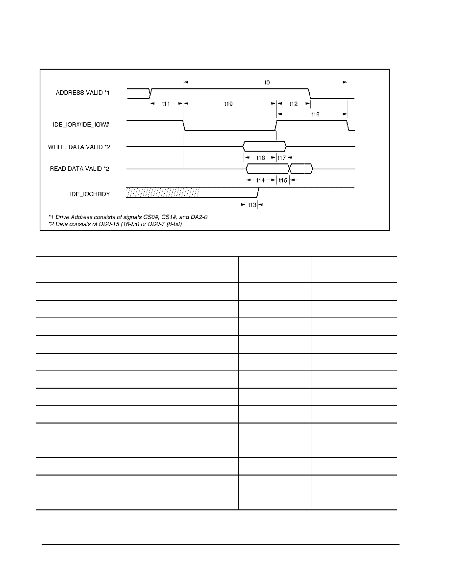
W83C553F Timing Diagrams
WINBOND SYSTEMS LABORATORY
140
Table 6-3. IDE Interface Timing
Parameter
Values
Min Max
Notes
t11 Address Setup to command low
3 x t1 ns -
t12 Address hold from command high
30ns
t13 IDE_IOCHRDY high setup to command high
0.5 x t1 ns
t14 Read data setup to IDE_IOR# high
10ns
t15 Read data hold from IDE_IOR# high
0ns
t16 Write data setup to IDE_IOW# high
t19ns
t17 Write data hold from IDE_IOW# high
30ns
t18 Command recovery time 8-bit cycle
300ns
t18 Command recovery time 16-bit cycle
r2 x t1ns
r2 is the 16-bit command
recovery count in PCI
clocks (page 126)
t19 Command active time 8-bit cycle
300ns
t19 Command active time 16-bit cycle
a2 x t1ns
a2 is the 16-bit command
active count in PCI clocks
(page 126)
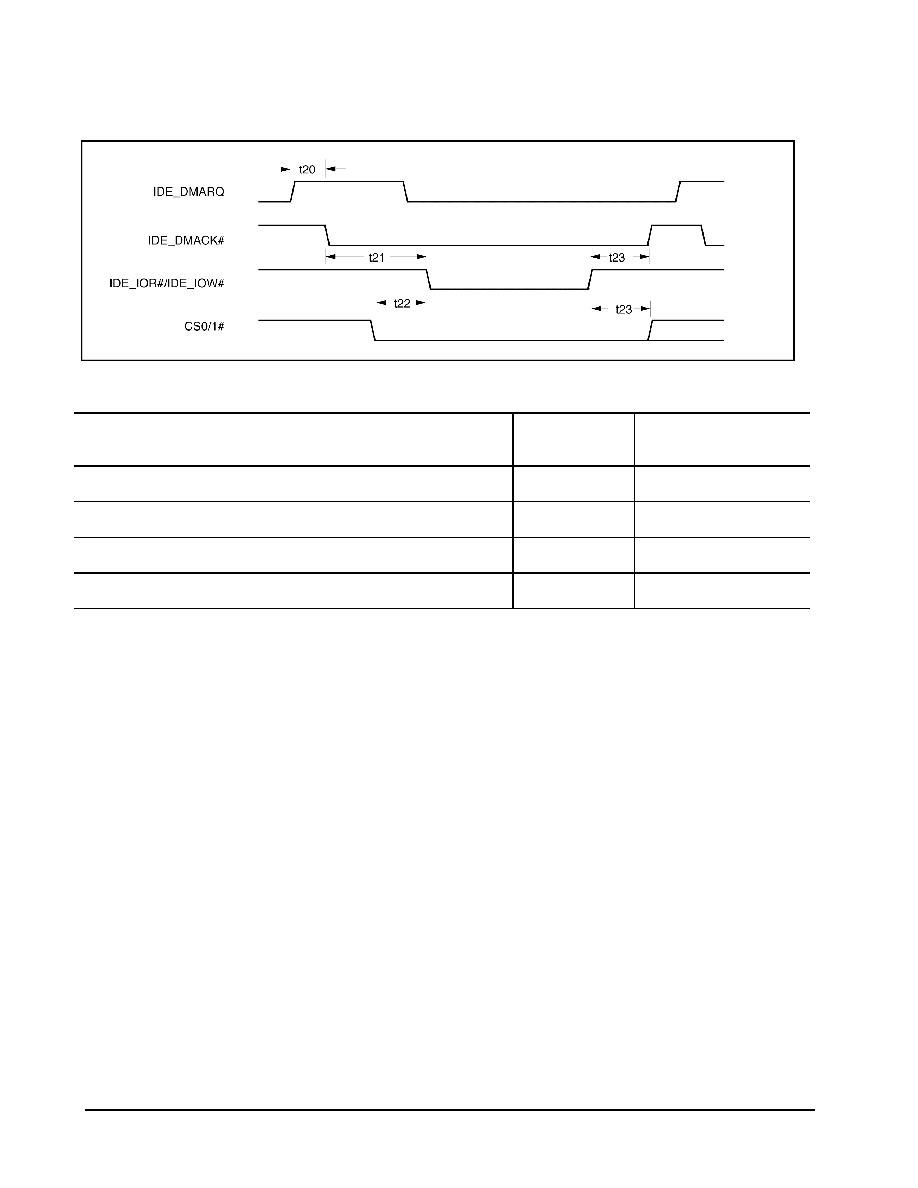
W83C553F Timing Diagrams
WINBOND SYSTEMS LABORATORY
141
Table 6-4. IDE Data Transfer Timing
Parameter
Values
Min Max
Notes
t20 IDEDRQ[A:B] high to IDEDAK[A:B]# low delay
0ns -
t21 IDEDAK[A:B]# setup to command low
0ns -
t22 CS0#, CS1# setup to command low
3 x t1ns
t23 IDEDAK[A:B]#, CS0#, CS1# hold from command high
t1ns
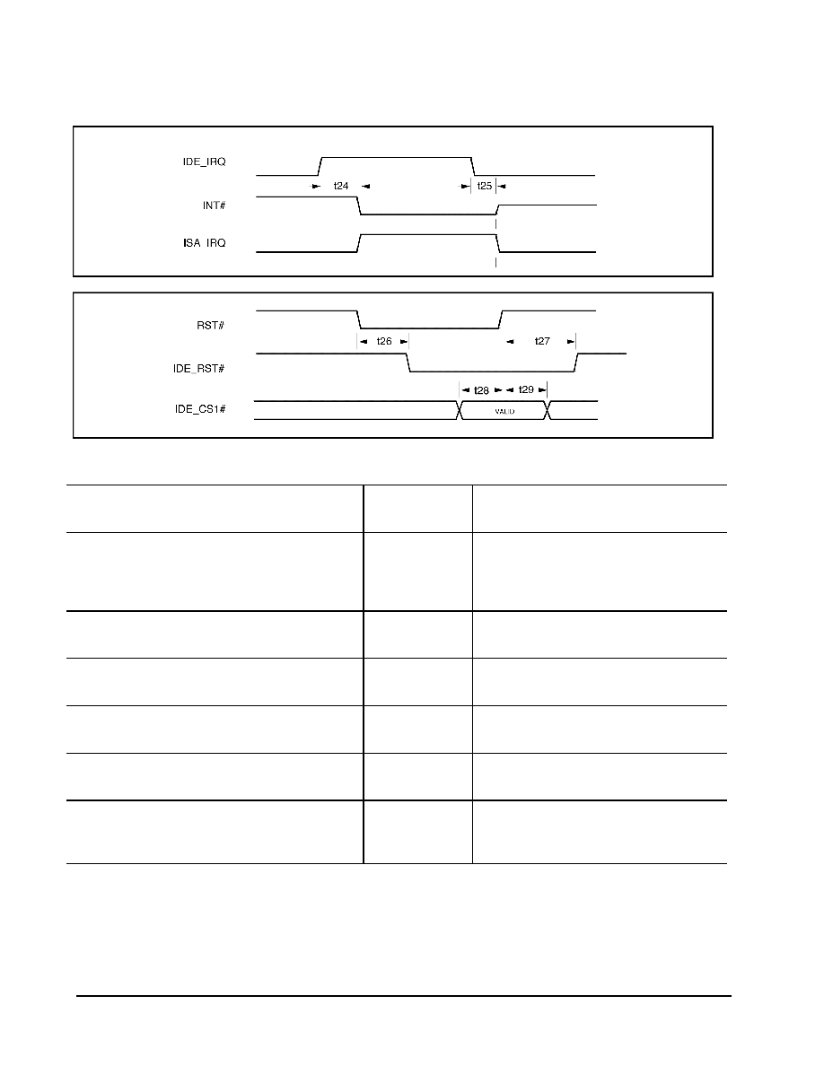
W83C553F Timing Diagrams
WINBOND SYSTEMS LABORATORY
142
Table 6-5. Miscellaneous Timing
Parameter
Values
Min Max
Notes
t24 IDEIRQ[A:B] high to INT# low
or ISA IRQ high
- 50ns
Assumes that the interrupt path is enabled.
It could be disabled or
temporarily delayed due to read data in a
FIFO.
t25 IDEIRQ[A:B] low to INT# float
or ISA IRQ low
- 50ns
t26 RST# low to IDE_RST# low
30ns 50ns
t27 RST# high to IDE_RST# high
- 50ns
t28 IDECS1# setup to
RST# high
20ns -
t29 IDECS1# hold from
RST# high.
0ns -
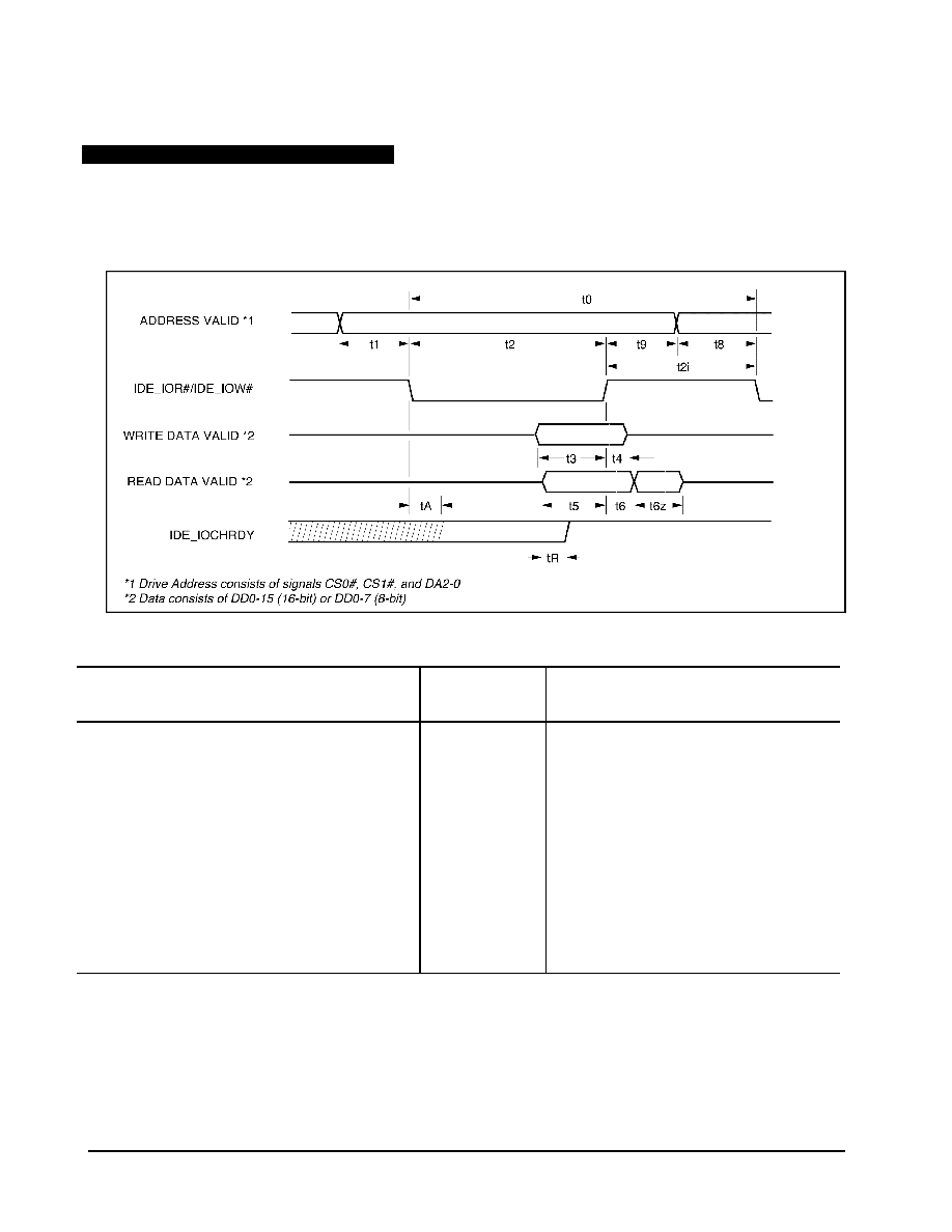
W83C553F Timing Diagrams
WINBOND SYSTEMS LABORATORY
143
6.2 IDE/ATA Data Transfers
This information has been transferred from the ATA-2 x3T9.2 specification for PIO modes 0-3, Multiword DMA modes 0-1
and Single-word DMA modes 0-2. SFF 8033 Rev. 0.2 defines PIO mode 4 and Multiword DMA mode 2.
6.2.1 Example PIO ATA Data Transfer Timing
Table 6-6. PIO ATA Data Transfer Timing
Parameter
Values
Min Max
Notes
t0 Cycle Time Mode 0
Mode 1
Mode 2
Mode 3
Mode 4
600ns
383ns
240ns
180ns
120ns
t1 Address valid to Mode 0
IDEIOR[A:B]# / IDEIOW[A:B]# Mode 1
setup Mode 2
Mode 3
Mode 4
70ns
50ns
30ns
30ns
25ns

W83C553F Timing Diagrams
WINBOND SYSTEMS LABORATORY
144
Table 6-6 (continued). PIO ATA Data Transfer Timing
Parameter
Values
Min Max
Notes
t2 IDEIOR[A:B]# / IDEIOW[A:B]# Mode 0
16-bit Mode 1
Mode 2
Mode 3
Mode 4
Mode 5
165ns
125ns
100ns
80ns
70ns
t0 is the minimum total cycle time, t2 is the
minimum command active time, and t2i is
the minimum command recovery time or
command inactive time. The actual cycle
time equals the sum of the actual command
t2 Pulse Width 8-bit Mode 0
Mode 1
Mode 2
Mode 3
Mode 4
Mode 5
290ns
290ns
290ns
80ns
70ns
active time and the actual command inactive
time. The three timing requirements of t0,
t2, t2i shall be met. The minimum total
cycle time requirement, t0, is greater than
the sum of t2 and t2i. This means host
implementation
t2i IDEIOR[A:B]# / IDEIOW[A:B]# Mode 0
recovery time Mode 1
Mode 2
Mode 3
Mode 4
Mode 5
-
-
-
70ns
25ns
can lengthen either or both t2 and t2i. to
ensure that t0 is equal to the value reported
in the devices identify drive data. A device
implementation shall support any legal host
implementation.
t3 IDEIOW[A:B]# Mode 0
data setup Mode 1
Mode 2
Mode 3
Mode 4
Mode 5
60ns
45ns
30ns
30ns
20ns
t4 IDEIOW[A:B]# data hold Mode 0
Mode 1
Mode 2
Mode 3
Mode 4
Mode 5
30ns
20ns
15ns
10ns
10ns

W83C553F Timing Diagrams
WINBOND SYSTEMS LABORATORY
145
Table 6-6 (continued). PIO ATA Data Transfer Timing
Parameter
Values
Min Max
Notes
t5 IDEIOR[A:B]# data setup Mode 0
Mode 1
Mode 2
Mode 3
Mode 4
Mode 5
50ns
35ns
20ns
20ns
20ns
t6 IDEIOR[A:B]# data hold Mode 0
Mode 1
Mode 2
Mode 3
Mode 4
Mode 5
5ns
5ns
5ns
5ns
5ns
t6z IDEIOR[A:B]# data Mode 0
tri-state Mode 1
Mode 2
Mode 3
Mode 4
Mode 5
-
-
-
30ns
30ns
This parameter specifies the time from the
negation edge of IDEIOR[A:B]# to the time
that the data bus is no longer driven by the
device (tri-state).
t9 IDEIOR[A:B]# / Mode 0
IDEIOW[A:B]# Mode 1
to address valid hold Mode 2
Mode 3
Mode 4
Mode 5
20ns
15ns
10ns
10ns
5ns
tR Read data valid to Mode 0
IDECHRDY active Mode 1
Mode 2
Mode 3
Mode 4
Mode 5
-
-
-
0ns
0ns
If IDE_IOCHRDY is initially asserted after
tA.
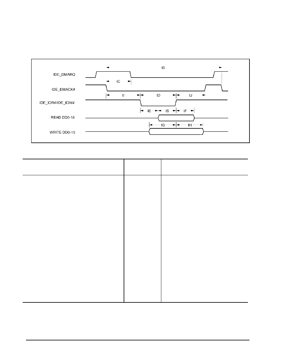
W83C553F Timing Diagrams
WINBOND SYSTEMS LABORATORY
146
6.2.2 Example Single Word DMA ATA Data Transfer Timing
Table 6-7. Single Word DMA ATA Data Transfer Timing
Parameter
Values
Min Max
Notes
t0 Cycle Time Mode 0
Mode 1
Mode 2
Mode 3
960ns
480ns
240ns
tC IDEDAK[A:B]# to Mode 0
IDEDRQ[A:B] delay Mode 1
Mode 2
Mode 3
200ns
100ns
80ns
tD IDEIOR[A:B]# / Mode 0
IDEIOW[A:B]# Mode 1
16-bit minimum Mode 2
command active time Mode 3
480ns
240ns
120ns
tE IDEIOR[A:B]# Mode 0
data access Mode 1
Mode 2
Mode 3
250ns
150ns
60ns

W83C553F Timing Diagrams
WINBOND SYSTEMS LABORATORY
147
Table 6-7 (continued). Single Word DMA ATA Data Transfer Timing
Parameter
Values
Min Max
Notes
tF IDEIOR[A:B]# Mode 0
read data hold Mode 1
Mode 2
Mode 3
5ns
5ns
5ns
tG IDEIOW[A:B]# Mode 0
write data setup Mode 1
Mode 2
Mode 3
250ns
100ns
35ns
tH IDEIOW[A:B]# Mode 0
write data hold Mode 1
Mode 2
Mode 3
50ns
30ns
20ns
tI IDEDAK[A:B]# to Mode 0
IDEIOR[A:B]# / Mode 1
IDEIOW[A:B]# setup Mode 2
Mode 3
0ns
0ns
0ns
tJ IDEIOR[A:B]# / Mode 0
IDEIOW[A:B]# to Mode 1
IDEDAK[A:B]# hold Mode 2
Mode 3
0ns
0ns
0ns
tS IDEIOR[A:B]# read setup Mode 0
Mode 1
Mode 2
Mode 3
tD-tEns -
tD-tEns -
tD-tEns -
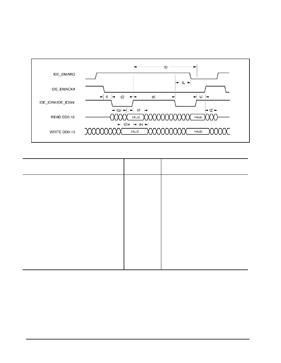
W83C553F Timing Diagrams
WINBOND SYSTEMS LABORATORY
148
6.2.3 Example Multiword DMA ATA Data Transfer Timing
Table 6-8. Multiword DMA ATA Data Transfer Timing
Parameter
Values
Min Max
Notes
t0 Cycle Time Mode 0
Mode 1
Mode 2
Mode 3
480ns
150ns
120ns
tC IDEDAK[A:B]# to Mode 0
IDEDRQ[A:B] delay Mode 1
Mode 2
Mode 3
-
-
-
tD IDEIOR[A:B]# / Mode 0
IDEIOW[A:B]# Mode 1
16-bit minimum Mode 2
command active time Mode 3
215ns
80ns
70ns

W83C553F Timing Diagrams
WINBOND SYSTEMS LABORATORY
149
Table 6-8 (continued). Multiword DMA ATA Data Transfer Timing
Parameter
Values
Min Max
Notes
tE IDEIOR[A:B]# Mode 0
data access Mode 1
Mode 2
Mode 3
150ns
60ns
-
tF IDEIOR[A:B]# Mode 0
read data hold Mode 1
Mode 2
Mode 3
5ns
5ns
5ns *
* The meaning of this parameter in ATA is
not clear. The parameter is not applicable to
this specification.
tZ IDEDAK[A:B]# Mode 0
to tri-state Mode 1
Mode 2
Mode 3
20ns
25ns
25ns
This parameter specifies the time from the
negation edge of DIOR# to the time that the
data bus is no longer driven by the device
(tristate).
tG IDEIOR[A:B]# / Mode 0
IDEIOW[A:B]# Mode 1
data setup Mode 2
Mode 3
100ns
30ns
20ns
tH IDEIOR[A:B]# / Mode 0
IDEIOW[A:B]# Mode 1
write data hold Mode 2
Mode 3
20ns
15ns
10ns

W83C553F Timing Diagrams
WINBOND SYSTEMS LABORATORY
150
Table 6-8 (continued). Multiword DMA ATA Data Transfer Timing
Parameter
Values
Min Max
Notes
tI IDEDAK[A:B]# to Mode 0
IDEIOR[A:B]# / Mode 1
IDEIOW[A:B]# Mode 2
setup Mode 3
0ns
0ns
0ns
tJ IDEIOR[A:B]# / Mode 0
IDEIOW[A:B]# to Mode 1
IDEDAK[A:B]# Mode 2
hold Mode 3
20ns
5ns
5ns
tKr IDEIOR[A:B]# negated Mode 0
pulse width Mode 1
Mode 2
Mode 3
50ns
50ns
25ns
The delay from DIOR# or DIOW# until the
state of IORDY is first sampled. If IORDY
is inactive, then the host shall wait until
IORDY is active before the PIO cycle can be
completed. If the device is not driving
IORDY negated at the time tA after the
activation of DIOR# or DIOW#, then t5
shall be met and tRD is not applicable. If
the device is driving IORDY negated at the
time tA after the activation of DIOR# or
DIOW#, then tRD shall be met and t5 is not
applicable.
tKw IDEIOW[A:B]# negated Mode 0
pulse width Mode 1
Mode 2
Mode 3
215ns
50ns
25ns
tLr IDEIOR[A:B]# to Mode 0
IDEDRQ[A:B] delay Mode 1
Mode 2
Mode 3
120ns
40ns
35ns
tLw IDEIOW[A:B]# to Mode 0
IDEDRQ[A:B] delay Mode 1
Mode 2
Mode 3
40ns
40ns
35ns
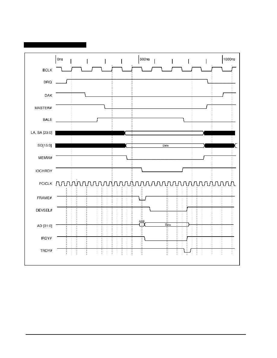
W83C553F Timing Diagrams
WINBOND SYSTEMS LABORATORY
151
6.3 ISA Bus Timing
Table 6-9. ISA Master Write to PCI
W83C553F Timing Diagrams
WINBOND SYSTEMS LABORATORY
152
Table 6-10. ISA Master Read from PCI
W83C553F Mechanical Description
WINBOND SYSTEMS LABORATORY
153
7.0 MECHANICAL DESCRIPTION
This chapter shows the dimensions of the W83C553F Enhanced SIO with PCI Arbiter chip.
208L QFP (28X28 mm footprint 2.6mm)
H
D
D
e
b
E
H
E
y
A
A
Seating Plane
L
L
1
See Detail F
Detail F
c
1
A
2
1
52
53
104
105
156
157
208
0.10
0
10
10
0
0.004
1.30
0.70
30.90
30.90
0.50
30.60
30.60
0.30
30.30
30.30
0.051
0.028
1.217
1.217
0.020
1.205
1.205
0.012
1.193
1.193
0.50
28.13
28.13
0.25
0.25
3.35
3.68
28.00
28.00
3.23
27.87
27.87
0.10
0.15
3.10
0.10
1.107
1.107
0.010
0.010
0.132
0.145
1.102
1.102
0.127
0.020
1.097
1.097
0.004
0.006
0.122
0.004
Symbol
Min
Nom
Max
Max
Nom
Min
Dimension in inch
Dimension in mm
A
b
c
D
e
H
D
H
E
L
y
A
A
L
1
1
2
E
0.008
0.006
0.15
0.20
0.016
0.043
0.024
0.059
0.40
0.60
1.10
1.50
control dimensions are in mm

W83C553F Thermal Information
WINBOND SYSTEMS LABORATORY
154
8.0 Thermal Information
Theta JA = Thermal Resistance between Junction and Ambient for the 208PQFP.
Theta JA = 43.13
0
C/W (air velocity = 0 M/s)
35.25
0
C/W(air velocity = 1 M/s)
30.90
0
C/W (air velocity = 2M/s)
Theta JA = (T
junction
- T
ambient
) / P
chip
;
Where P
chip
= Power dissipation on the chip (in watts)

W83C553F Appendix A
WINBOND SYSTEMS LABORATORY
155
Driving capacity of output and input/output pins of 553F (Revision G)
Pin Name
Pin #
I/O
Output Cur.
Note
A20M#/PCIRST#
22
Output
PCI Std.
Note 1
AD[31:0]
29-31, 33-37, 41-44, 46, 47,
49, 50, 62-67, 69, 71, 73-79,
81
Input/Output
C/BE[3:0]#
39, 51, 61, 72
Input/Output
PCI Std.
PAR
60
Input/Output
PCI Std.
FRAME#
53
Input/Output
PCI Std.
PERR#
58
Input/Output
PCI Std.
IRDY#
54
Input/Output
PCI Std.
TRDY#
55
Input/Output
PCI Std.
DEVSEL#
56
Input/Output
PCI Std.
STOP#
57
Input/Output
PCI Std.
SERR#
59
Input/OD
PCI Std.
INT[C:D]#
19, 18
Input/OD
PCI Std.
GNT0#/PIBREQ#
26
Output
8 mA
Note 3
GNT1#/IDEREQ#
28
Output
8 mA
ARBDIS#/GNT2#
16
Input/Output
8 mA
PCI5TH#/GNT3#
13
Input/Output
8 mA
GNT4#/FLSHREQ#
6
Output
8 mA
PWRPC/X86#/CPUGNT#
8
Input/Output
6 mA
IDECS0#
87
Output
24 mA
IDECS1#/NAT/LEG#
86
Input/Output
24 mA
IDEIOWA#
85
Output
24 mA
IDEIORA#
83
Output
24 mA
IDEIOWB#
84
Output
24 mA
IDEIORB#
82
Output
24 mA
IDEDAKA#
94
Output
24 mA
IDEDAKB#
93
Output
24 mA
DA[2:0]
88, 90, 89
Output
24 mA
DD[15:0]
98, 101, 103, 105, 108, 110,
112, 114, 115, 113, 111,
109, 106, 104, 102, 100
Input/Output
24 mA
BCLK
200
Output
Clock Std.
Note 2
LA[23:17]
176, 178, 180, 182, 184,
187, 189
Input/Output
24 mA
SA[16:0]
144, 145, 147-149, 151,
152, 155, 158, 160, 162,
164, 165, 167, 169, 171, 173
Input/Output
24 mA
REFRESH#
150
Input/Output
24 mA
MEMR#
141
Input/Output
24 mA
MEMW#
142
Input/Output
24 mA
IOR#
140
Input/Output
24 mA
IOW#
139
Input/Output
24 mA
SMEMR#
138
Output
24 mA
SMEMW#
137
Output
24 mA
SBHE#
174
Input/Output
24 mA
M16#
175
Input/Output
24 mA

W83C553F Appendix A
WINBOND SYSTEMS LABORATORY
156
IOCHRDY
135
Input/Output
24 mA
BALE
168
Output
24 mA
AEN
136
Output
24 mA
TC
166
Output
24 mA
DAK[2:0]
194, 192, 195
Output
24 mA
PMACT#/ISARST
5
Output
16 mA
SD[15:0]
208-204, 202, 199, 197,
123, 125, 126, 128-131, 133
Input/Output
24 mA
SECURITY/XDR#
116
Input/Output
24 mA
XOE#
117
Input/Output
24 mA
XCS0/ROMCS
119
Output
24 mA
XCS1/X8XCS
118
Output
24 mA
INT
10
Output
4 mA
NMI
11
Output
4 mA
INIT
3
Output
4 mA
SPKR
134
Output
24 mA
IGNNE#/HRESET#
4
Output
6 mA
Note 1: The driving capacity of these I/O cells is based on PCI specification
Note 2: This is the clock output buffer.
Note 3: At this current, V
OLmax
<= 0.4V,
V
OHmin
>= 3.0V