 | –≠–ª–µ–∫—Ç—Ä–æ–Ω–Ω—ã–π –∫–æ–º–ø–æ–Ω–µ–Ω—Ç: W89C926 | –°–∫–∞—á–∞—Ç—å:  PDF PDF  ZIP ZIP |

Preliminary W89C926 PENTIC+
PCMCIA ETHERNET NETWORK
TWISTED PAIR INTERFACE CONTROLLER
Publication Release Date: January 1996
- 1 -
Revision A1
GENERAL DESCRIPTION
The W89C926 PENTIC+ is a CMOS device designed for easy implementation of PCMCIA R2.1
compatible CSMA/CD local area networks. The W89C926 combines a W89C902 Serial LAN
Coprocessor for Twisted-pair (SLCT) with a PCMCIA Bus Interface (PBI), thus integrating into
a single chip all the registers and logic necessary to connect the SLCT to buffer SRAMs, flash
memories (or an EEPROM), and the PCMCIA system bus.
The PCMCIA Bus Interface (PBI) is designed to provide a switchless setting architecture that allows
the card setting to be configured by software. It implements a full set of PCMCIA registers for
PCMCIA R2.1 compatibility and a set of configuration registers for switchless card setting. The card
can be configured quickly and easily by modifying the contents of the configuration registers. The
PENTIC+ can run with shared memory mode and NE2000
TM
I/O mode drivers on a 16-bit bus
interface. No extra effort is needed to ensure software compatibility.
The PENTIC+ provides a flexible flash memory (up to 128 KB)/EEPROM (up to 512 bytes)
architecture for PCMCIA nonvolatile storage and an ID/Configuration auto-load architecture for
power-on initialization. Vendors can store the Ethernet
Æ
ID, configuration, and CIS in the flash
memory or EEPROM. The PENTIC+ will auto-load necessary information when power is switched on.
FEATURES
∑
Runs with NE2000
TM
or shared memory drivers
∑
Supports up to 128 KB flash memory (8K/112K for attribute/common memory) or 512 bytes
EEPROM (for attribute memory only) for nonvolatile memory
∑
Uses one 16 KB SRAM or one 32 KB SRAM (if EEPROM is used) for 16 KB Ethernet ring buffer
∑
Auto-load algorithm provided for power-on initialization
∑
Supports necessary PCMCIA registers
∑
Configuration registers allow switchless card setting
∑
UTP/BNC auto media-switching function provided
∑
Drives necessary LEDs for network status display
∑
Single 5V power supply with low power consumption
∑
100-pin thin package (TQFP) fits into PCMCIA Type II profile
Ethernet
Æ
is a registered trademark of the Xerox Corporation.
NE2000
TM
is a trademark of Novell, Inc.
W89C926 PENTIC+
- 2 -
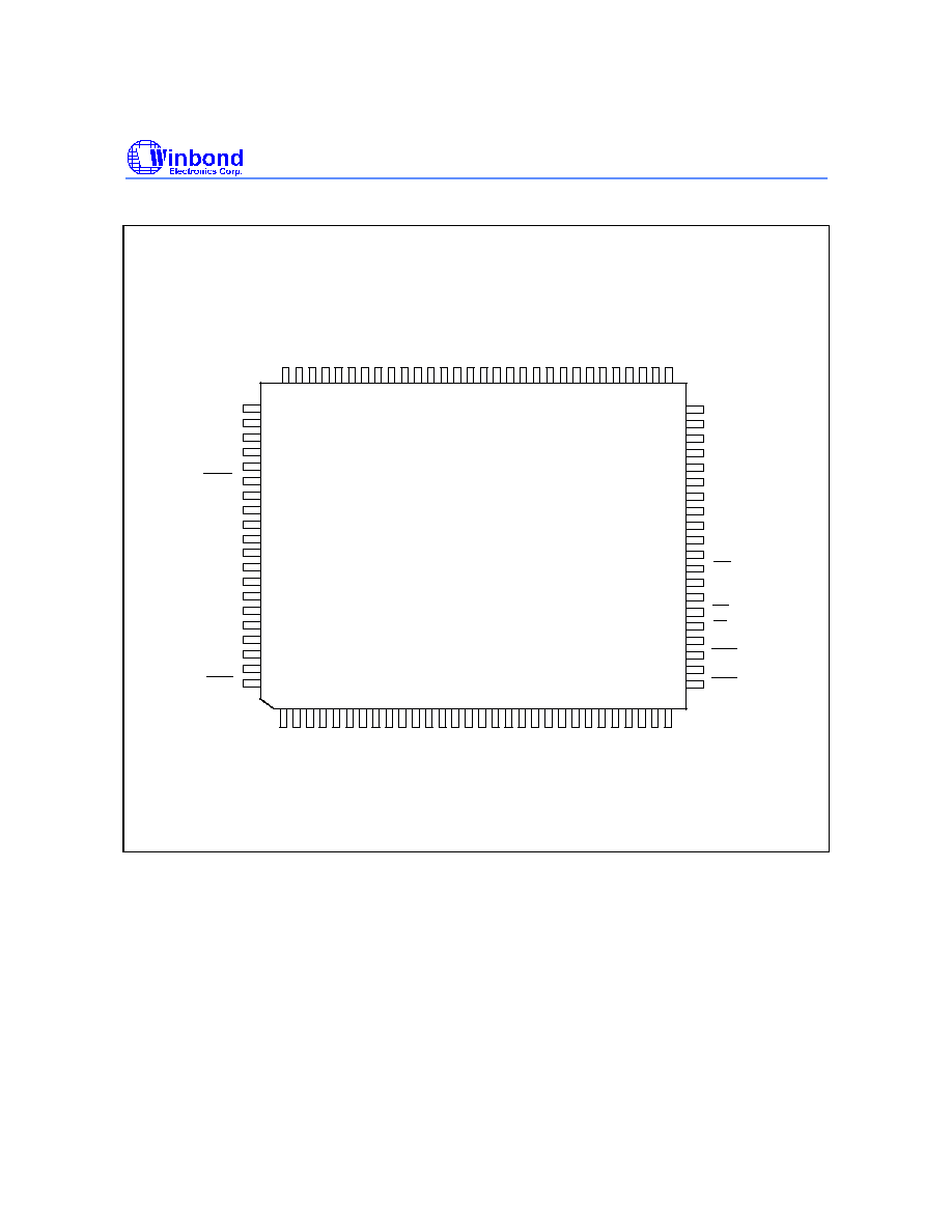
PIN CONFIGURATION
32
31
1
2
3
4
5
6 7
8
9
1
0
1
1
1
2
1
3
1
4
1
5
1
6
1
7
1
8
1
9
2
0
2
1
2
2
2
9
2
3
2
4
2
5
2
6
2
7
2
8
3
0
33
34
35
36
37
38
39
40
41
42
43
44
45
46
47
48
49
50
5
1
5
2
5
3
5
4
5
5
5
6
5
7
5
8
5
9
6
0
6
1
6
2
6
3
6
4
6
5
6
6
6
7
6
8
6
9
7
0
7
1
7
2
7
3
7
4
7
5
7
6
7
7
7
8
7
9
8
0
81
82
83
84
85
86
87
88
89
90
91
92
93
94
95
96
97
98
99
100
.
H
D
1
0
H
D
2
V
C
C
H
D
9
G
N
D
H
D
1
H
D
0
H
A
0
H
D
8
H
A
1
/
R
E
G
H
A
2
/
I
N
P
A
C
K
D
G
N
D
H
A
3
D
V
C
C
/
W
A
I
T
H
A
4
H
A
5
H
A
6
R
E
S
E
T
H
A
1
2
H
A
1
5
H
A
7
/
I
R
E
Q
H
A
1
6
H
A
1
4
/
W
E
H
A
1
3
H
A
8
IOWR
HA9
IORD
HA11
OE
CE2
HA10
HD15
CE1
HD14
HD7
HD13
GND
HD6
HD12
HD5
HD11
HD4
HD3
T
H
I
N
R
X
I
+
R
X
I
-
G
N
D
X
1
X
2
/
G
D
L
N
K
/
A
C
T
L
E
D
M
S
A
1
5
C
D
+
C
D
-
R
X
+
T
X
+
T
X
-
R
X
-
T
X
O
+
T
X
O
-
A
G
N
D
M
S
A
1
6
M
S
D
3
M
S
D
4
M
S
D
5
M
S
D
6
M
S
D
7
E
E
C
S
,
/
F
C
S
/
R
C
S
M
S
A
1
0
/
M
S
R
D
M
S
A
1
1
A
V
C
C
V
CC
MSA8
MSA13
MSWR
MSD0
MSA1
MSA3
MSA9
GND
MSD2
MSD1
MSA0
MSA2
MSA4
MSA5
MSA6
MSA7
MSA12
MSA14
IOS16
V
CC
W89C926 PENTIC+
Publication Release Date: January 1996
- 3 -
Revision A1
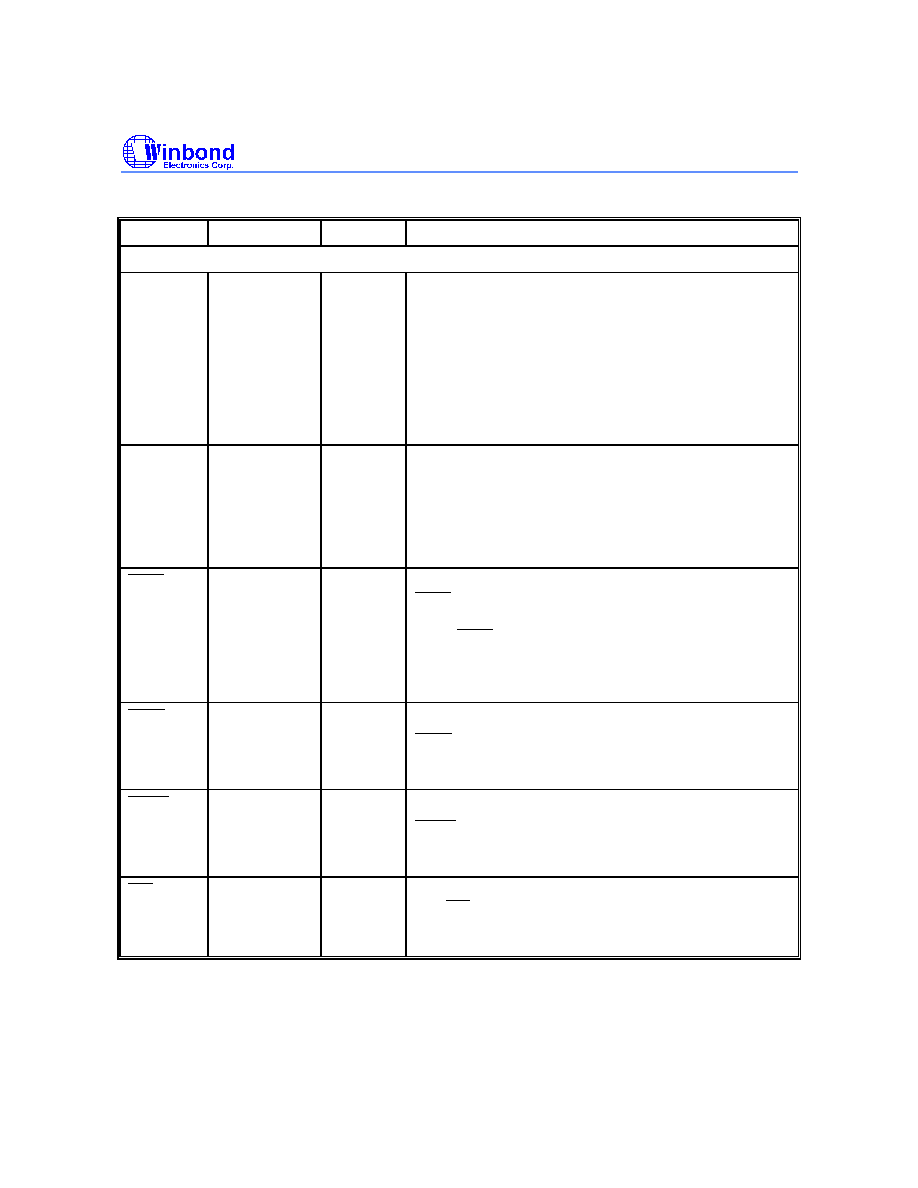
PIN DESCRIPTION
NAME
NUMBER
TYPE
DESCRIPTION
PCMCIA Bus Interface
HA0-2
HA3, 4
HA5-7
HA8-10
HA11-13
HA14-16
9, 10, 12
15, 18
20-22
30, 32, 37
34, 23,29
28, 24, 25
I/TTL
Host Address Bus:
Host address lines used to decode access to the card's
memory and I/O spaces.
HD0-2
HD3-5
HD6-8
HD9-11
HD12-15
8, 6, 2
50, 49, 47
44, 41, 7
4, 1, 48
46, 42, 40, 38
IO/3SH
Host Data Bus:
Bidirectional host data bus.
IREQ
26
O/TTL
Interrupt Request:
IREQ is asserted by the PENTIC+ to request host
service. During auto-loading, which is caused by a H/W
reset, IREQ will assert low until auto-loading is
complete. This signaling is used as Rdy/-Bsy of
Memory Only Interface during initialization, according to
PCMCIA R2.1.
IORD
33
I/TTL
I/O Read:
IORD is asserted by the system to read data from the
card's I/O space. It has an internal 100K ohm pull-high
resistor.
IOWR
31
I/TTL
I/O Write:
IOWR is asserted by the system to write data to the
card's I/O space. It has an internal 100K ohm pull-high
resistor.
WE
27
I/TTL
Write Enable:
The WE input is asserted by the system to strobe
memory write data into the card memory. It has an
internal 100K ohm pull-high resistor.
W89C926 PENTIC+
- 4 -
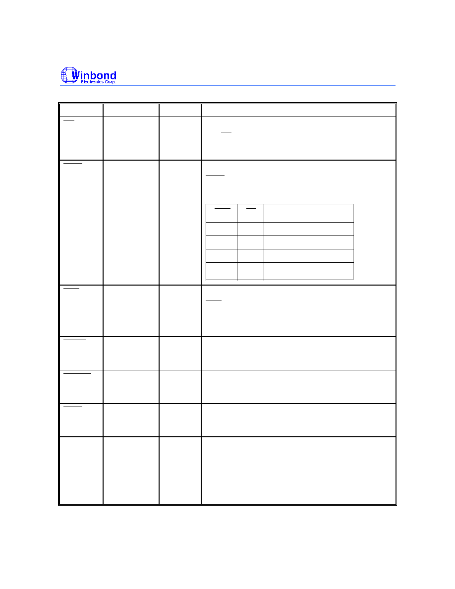
Pin Description, continued
NAME
NUMBER
TYPE
DESCRIPTION
OE
35
I/TTL
Output Enable:
The OE line is asserted by the system to obtain
memory read data from the card memory. It has an
internal 100K ohm pull-high resistor.
CE1,2
39, 36
I/TTL
Card Enable:
CE1,2
are asserted by the system for data bus width
control as shown below. These pins have an internal
100K ohm pull-high resistor.
CE2
CE
HD15-HD8
HD7-HD0
0
0
1
1
0
1
0
1
Valid
Valid
High-Z
High-Z
Valid
High-Z
Valid
High-Z
REG
11
I/TTL
Register & I/O selection:
REG is asserted by the system to access attribute
memory or I/O space. It remains high inactive for
common memory accesses. It has an internal 100K ohm
pull-high resistor.
IOIS16
100
O/TTL
16-bit I/O access:
Asserted by the PENTIC+ to inform the system that
current operation is a 16-bit I/O access.
INPACK
13
O/TTL
Input Acknowledge:
Asserted by the PENTIC+ when it has been selected
and can respond to an I/O read cycle.
WAIT
17
O/TTL
Wait State:
Asserted by the PENTIC+ to insert wait states into
current memory or I/O access cycles.
RESET
19
I/TTL
Card Reset:
A RESET pulse will initiate the PENTIC+'s initialization
procedure, including auto-ID/configuration loading,
register initialization, and state machine initialization.
The pulse width should be at least 500 nS to be
recognized as a valid reset. This pin has an internal
100K ohm pull-up resistor.

W89C926 PENTIC+
Publication Release Date: January 1996
- 5 -
Revision A1
Pin Description, continued
NAME
NUMBER
TYPE
DESCRIPTION
Memory Support Interface
MSA0-7
MSA8-10
MSA11-13
MSA14-16
90-97
82, 81, 78
80, 98, 84
99, 69, 70
O/TTL
Memory Support Address:
Latched address used to decode accesses to the on-
board memory.
MSD0-2
MSD3-7
89-87
71-75
IO/3SH
I/O/3SH
Memory Support Data Bus:
Bidirectional on-board memory data bus.
EEPROM Interface:
During the EEPROM auto-load or read/write sequence,
MSD0 is used as a serial data input/output from/to
EEPROM, MSD1 outputs EEPROM commands to
EEPROM, and MSD2 sends a clock with a period of 1.2
microseconds. This function is available only when
EECS/ FCS is low during H/W reset.
RCS
77
O/TTL
SRAM Chip Select:
RCS
is asserted by the PENTIC+ for SRAM chip
enable during buffer memory access.
EECS/
FCS
76
O/3SH
I/3SH
Nonvolatile Memory Chip Select:
EECS/ FCS is asserted by the PENTIC+ for chip enable
during nonvolatile memory access. It is active low for
flash memory enable and active high for EEPROM chip
enable.
Nonvolatile Memory Detection:
During H/W reset, the PENTIC+ will determine the
existing nonvolatile memory type by sampling the
voltage level on this pin. If this pin is externally pulled
high with a 470K ohm resistor, the PENTIC+ will
determine that the memory is a flash memory; if the pin
is pulled low with a 470K ohm resistor, it will determine
that the memory is an EEPROM.
MSRD
79
O/TTL
Memory Support Read:
MSRD
is asserted by the PENTIC+ to strobe read data
from the on-board memory. Both SRAM and flash
memory use
MSRD
as the read command strobe.