W89C92
TRANSCEIVER FOR COAXIAL CABLE (TCC)
Publication Release Date: September 1994
- 1 -
Revision A3
GENERAL DESCRIPTION
The W89C92 Transceiver for Coaxial Cable (TCC) serves as an interface between the Attachment
Unit Interface and coaxial cable and implements the MAU functions required by a 10BASE2 or
10BASE5. The W89C92 provides transmit, receive, jabber lockup, SQE test, and collision presence
functions.
The W89C92 provides a functional solution for a 10BASE2 or 10BASE5 MAU. The power isolation
requirement of the MAU is met by using a DC-to-DC converter and a one-to-one ratio transformer.
FEATURES
∑
Compatible with IEEE 802.3 10BASE2 and 10BASE5
∑
CMOS process provides low power consumption
∑
Mixed-mode circuit design integrates all transceiver electronics except signal and power isolation
and minimizes external component count
∑
On-chip jabber timer and state machine meet the requirements for IEEE 802.3 MAU function
∑
External selective SQE test function allows operation with IEEE 802.3 compatible repeater
∑
Precision detection circuit design implements transmit mode collision detection
∑
External selective jabber lockup function allows infinite data transmission
∑
Standard 16-pin DIP and 28-pin PLCC package provide easy implementation of a MAU
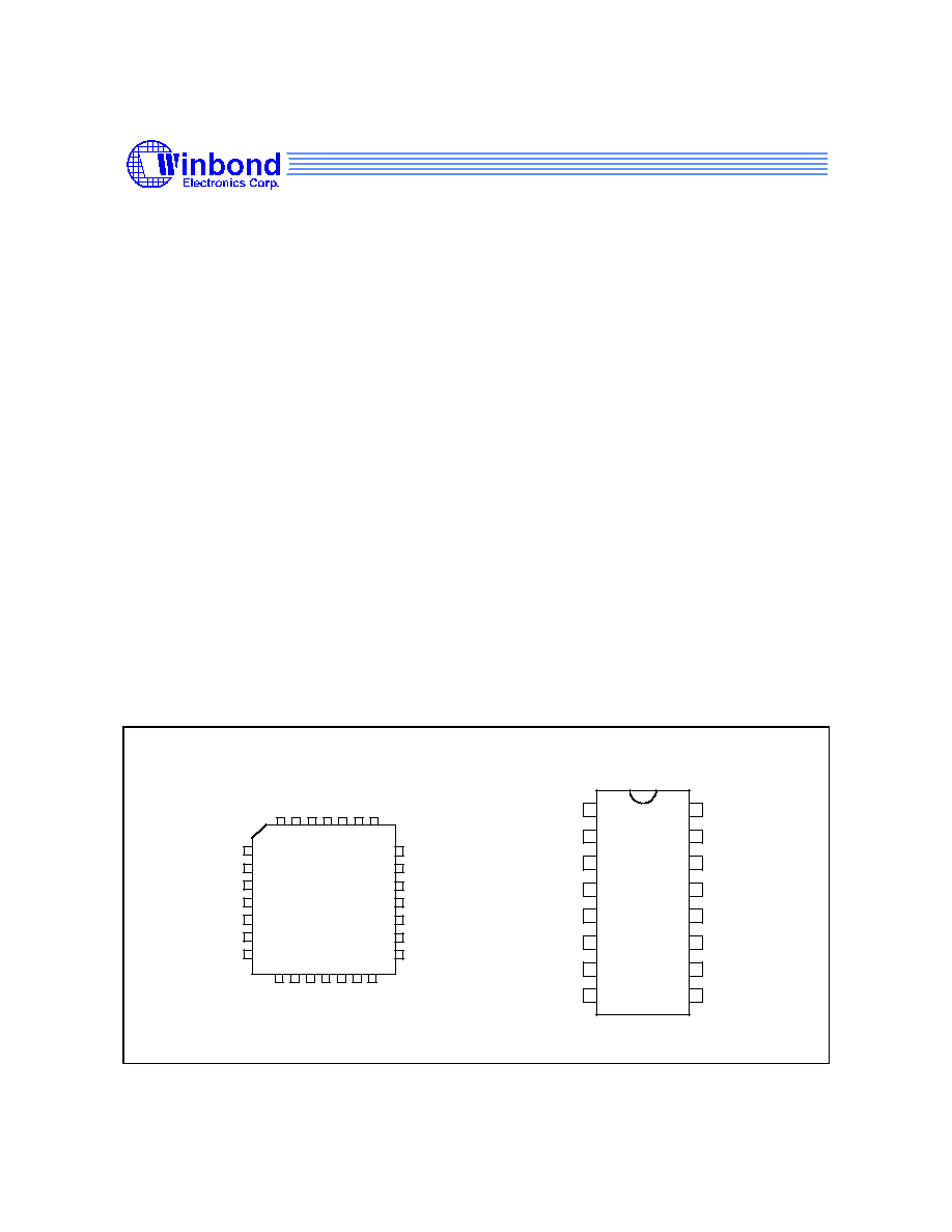
PIN CONFIGURATIONS
1
16
CLS
CSO+
CSO-
DI+
SS
V
2
3
4
5
6
11
12
13
14
15
V
RXI
TXO
ER+
7
8
10
SQE
DO+
DO-
9
SS
ER-
V
DD
SS
V
DI-
5
6
7
8
22
23
24
25
19
20
21
9
10
11
ER-
V
SS
V
SS
V
SS
V
SS
V
SS
V
SS
V
SS
V
SS
V
SS
V
SS
V
SS
V
SS
V
SS
V
D
D
V
D
D
D
O
+
D
O
-
S
Q
E
E
R
+
26
27
28
1
2
3
4
D
I
+
C
S
O
-
C
S
O
+
C
L
S
T
X
O
N
C
R
X
I
12 13 14 15 16 17 18
D
I
-

W89C92
- 2 -
PIN DESCRIPTION
Attachment Unit Interface Pins
CSO+, CSO- (DIP 1, 2/PLCC 2, 3) (O/P): Collision Output Positive, Collision Output Negative
CSO+/CSO- are a differential signal pair that drives 10 MHz signals to the DTE (data transmit
equipment) when a collision is detected on the segment, the DTE transmits an excessively long
packet, or the cable is disconnected. CSO+/CSO- are also active for a period of time after the end of
every transmission. CSO+ and CSO- should be pulled down by a 510 ohm resistor.
DI+, DI- (DIP 3, 6/PLCC 4, 12) (O/P): Data-in Output Positive, Data-in Output Negative
DI+/DI- are also a differential signal pair. Signals received from the network segment that meet the
bandwidth requirement and carrier sense levels will be transferred into differential format and driven
out from DI+/DI-. A 510 ohm pull-down resistor is also required for DI+/DI-.
DO+, DO- (DIP 7, 8/PLCC 13, 14) (I/P): Data-out Input Positive, Data-out Input Negative
Data transmitted from the DTE are received on DO+/DO- and transferred into a current signal on the
coaxial cable.
Coaxial Media Interface Pins
TXO (DIP 15/PLCC 28) (O/P): Transmit Output
The current signal on the coaxial cable is sunk into TXO. TXO is pulled up to V
DD
internally. A diode
should be used to isolate the TXO capacitance loading from the coaxial cable.
RXI (DIP 14/PLCC 26) (I/P): Receive Input
The signal on RXI is filtered by a low-pass filter and transferred to DI+/DI- with differential format. The
RXI should be connected directly to the coaxial cable.
CLS (DIP 16/PLCC 1) (I/P): Collision Sense Input
The collision detection threshold is determined by the level of the CLS pin. The transmit mode
collision detection of 10BASE2 is implemented when CLS is connected directly to V
DD
.
Control Pins
ER+, ER- (DIP 11, 12/PLCC 18, 19) (I/P): External Resistor Positive, External Resistor Negative
A fixed 1K 1% ohm resistor should be connected between ER+ and ER- to establish the internal
operating current.
SQE (DIP 9/PLCC 15) (I/P): Signal Quality Error Test
The signal quality error test will be enabled when SQE is tied to V
DD
. The jabber lockup function can
be disabled by changing the SQE bias.
Power Pins
V
DD
(DIP 10/PLCC 16, 17) (I/P): Positive Power Supply
A9 VDC power supply is needed.
V
SS
(DIP 4, 5, 13/PLCC 5 to 11, 20 to 25) (I/P): Negative Power Supply

W89C92
Publication Release Date: September 1994
- 3 -
Revision A3
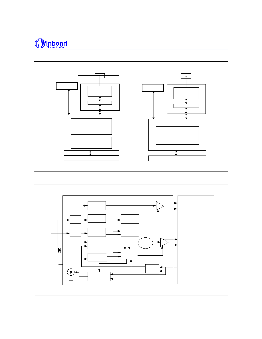
SYSTEM DIAGRAM
Coax.
Twisted pair
Line
W89C92
Transceiver
for
Coax. Cable
W89C902
Bus
Interface
Controller
Host Bus
Isolation
Twisted pair
Line
Coax.
W89C92
Transceiver
for
Coax. Cable
W89C905
Host Bus
Isolation
TELISA
BLOCK DIAGRAM
Equalizer
Amplifier
4-pole Bessel
Low Pass filter
4-pole Bessel
Low Pass filter
SQE Heartbeat
Generator
Jabber
Timer
Line
Driver
Receiver
Squelch
Collision
Threshold
State
Machine
Transmit
Squelch
Buffer
Buffer
10 MHz
Oscillator
TX
TXB
CD
CDB
RX
RXB
RXI
CDS
GND
HBE
TXO
DI+
DI-
CSO+
CSO-
DO+
DO-

W89C92
- 4 -
FUNCTIONAL DESCRIPTION
Transmit Function
The W89C92 transmits data received from the DTE onto the coaxial cable in a current format. The
signal current is sunk from the coaxial cable. The internal current control switch responds to the
activity of the DTE (DO+/DO-) output data. DTE differential output signals meeting the squelch
threshold will be decoded into digital signals without logical inversion to control the internal current
switch. The transmitter output is pulled up to V
DD
when the current sink source is turned off.
Receive Function
The W89C92 translates signals on the coaxial cable into differential signal format and sends the data
to the DTE. The AC component of the coaxial cable signal carries the data message and is converted
into a digital signal format. The differential pair driver (DI+/DI-) then sends a differential signal
corresponding to the AC signal on the coaxial cable. The receiver of the W89C92 receives the signal
on the coaxial cable regardless of whether the signal is sent by the W89C92 itself or by another MAU.
The receiver of the W89C92 performs a loopback function when the W89C92 is transmitting.
Jabber Lockup Function
The W89C92 will inhibit its transmitter when the transmitter is activated for a time longer than the
jabber activation delay. Excessively long packets sent from the DTE cannot be sent out completely if
the packet length exceeds the jabber activation delay. The jabber lockup function protects the
network segment from a malfunctioning station or invalid traffic requirements. The jabber lockup
function can be disabled for certain special applications, such as when an infinite data packet is to be
transmitted. In a 9V DC power system, the jabber lockup function may be disabled by setting the SQE
pin to between
-3.4V and -5.4V.
Collision Presence Function
A collision condition occurs when two or more stations are transmitting data at the same time. The
W89C92 detects collision conditions by monitoring the DC level of the signal on the coaxial cable. A
signal with a DC level lower than the collision threshold forces the W89C92 to send the collision
signal (a 10 MHz differential signal) on CSO+/CS0-. The collision detection scheme of the W89C92
meets the transmit mode requirements specified by the IEEE 802.3 10BASE2 MAU function. The
CSO+/CSO- differential pair driver is also active when the coaxial cable is disconnected.
SQE Test Function
The W89C92 implements the SQE test function by sending out a collision signal from CSO+/CSO-
for a short time CSO+/CSO- after the end of every transmission. The SQE test function can be
disabled to meet the IEEE 802.3 repeater unit requirements. The SQE test function remains enabled
when the jabber lockup function is disabled.
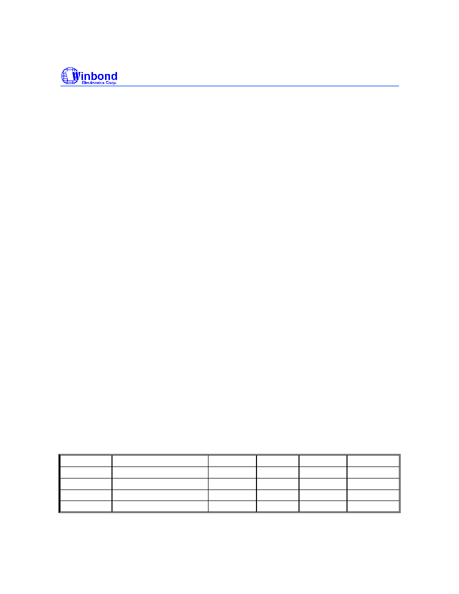
ABSOLUTE MAXIMUM RATINGS
SYMBOL
DESCRIPTION
MIN.
TYP
MAX.
UNIT
T
A
Ambient temperature
0
-
70
∞
C
T
S
Storage temperature
-65
-
150
∞
C
V
SS
Supply voltage
-
-
-12
V
V
IN
Input voltage
0
-
-12
V
Note: Exposure to conditions beyond those listed under Absolute Maximum Ratings may adversely affect the life and reliability of the
device.

W89C92
Publication Release Date: September 1994
- 5 -
Revision A3
DC CHARACTERISTICS
(V
SS
= -9V
±
5%, Ta = 0
∞
C to 70
∞
C) (Notes 1, 2)
SYMBOL
DESCRIPTION
MIN.
TYP
MAX.
UNIT
V
CD
Collision threshold (in transmit mode)
-1.43
-1.53
-1.70
V
V
DO
Differential output voltage
±
500
±
800
±
1500
mV
V
DOI
Diff. output voltage imbalance
-
-
±
60
mV
V
CMO
Diff. common mode output voltage
-3.0
-3.5
-4.0
V
V
TS
DO+/DO- transmit squelch threshold
-175
-225
-330
mV
I
SSN
Supply current out of V
SS
(non-transmitting)
-
-80
-100
mA
I
SST
Supply current out of V
SS
(transmitting)
-
-120
-150
mA
I
RXI
Receive input bias current
-1
-
+1
µ
A
I
TDC
Transmit out current DC level
37
41
45
mA
I
TAC
Transmit out current AC level
±
30
-
±
I
TDC
mA
R
RXI
RXI shunt resistance non-transmitting
-
5
-
M
R
TXO
TXO shunt resistance transmitting
7.5
10
-
K
C
RXI
RXI shunt capacitance
-
1.2
-
pF
AC CHARACTERISTICS
(V
SS
= -9V
±
5%, Ta = 0
∞
C to 70
∞
C) (Notes 1, 2)
SYMBOL
DESCRIPTION
MIN.
TYP
MAX.
UNIT
T
CON
Collision turn-on delay
7
8
9
bits
T
COFF
Collision turn-off delay
10
bits
F
CD
Collision signal frequency
8
12
MHZ
T
CP
Collision signal pulse width
35
70
nS
T
SQEON
SQE test turn-on delay
0.6
1.4
µ
S
T
SQED
SQE test duration
0.8
1.0
1.5
µ
S
T
JA
Jabber activation delay
20
60
mS
T
JR
Jabber recovery time
250
750
mS
T
TST
Transmit start-up delay
1
2
bits
T
TD
Transmit propagation delay
25
60
nS
T
TR
Transmit rise time, 10% to 90%
25
nS
T
TF
Transmit fall time, 90% to 10%
25
nS
