
Preliminary W91030B
CALLING LINE IDENTIFIER
Publication Release Date: March 2000
- 1 - Revision A1
Table of Contents-
GENERAL DESCRIPTION ..............................................................................................................................2
FEATURES......................................................................................................................................................2
PIN CONFIGURATION ....................................................................................................................................3
PIN DESCRIPTION..........................................................................................................................................3
SYSTEM DIAGRAM ........................................................................................................................................5
BLOCK DIAGRAM ...........................................................................................................................................5
FUNCTIONAL DESCRIPTION ........................................................................................................................6
Ring Detector.................................................................................................................................................6
Input Pre-processor .......................................................................................................................................7
Dual Tone Alert Signal Detection....................................................................................................................7
FSK Demodulation.........................................................................................................................................9
Other Functions ...........................................................................................................................................11
ELECTRICAL CHARACTERISTICS..............................................................................................................13
Absolute Maximum Ratings .........................................................................................................................13
Recommended Operating Conditions...........................................................................................................13
DC Electrical Characteristics........................................................................................................................13
Electrical Characteristics - Gain Control OP-Amplifier ..................................................................................15
AC Electrical Characteristics........................................................................................................................15
AC Timing Characteristics ...........................................................................................................................16
APPLICATION INFORMATION .....................................................................................................................21
Application Circuit........................................................................................................................................21
Application Environment ..............................................................................................................................23
PACKAGE DIMENSIONS..............................................................................................................................29
The information described in this document is the exclusive intellectual property of Winbond Electronics Corporation and
shall not be reproduced without permission from Winbond.
Winbond provides this document for reference purposes of W-based system design only. Winbond assumes no responsibility
for errors or omissions. All data and specifications are subject to change without notice.

Preliminary W91030B
- 2 -
GENERAL DESCRIPTION
The Winbond Caller Identification device W91030B, is a low power CMOS integrated circuit used to
receive physical layer signals transmitted according to Bellcore and British Telecom (BT)
specifications. There are two types of Caller Identifications, the first type is on-hook calling with caller
ID message and the second type is call on waiting. The W91030B device provides all the features
and functions of the Caller Identification specification for both these types, including FSK
demodulation, Tone Alert Signal detection and ring detection. The FSK demodulation function can
demodulate Bell 202 and CCITT V.23 Frequency Shift Keying (FSK) with 1200 baud rate. The Tone
Alert Signal detect function can detect the dual tones of the Bellcore CPE* Tone Alerting Signal
(CAS) and the BT idle State and Loop State Tone Alert Signal. The line reversal for BT, ring burst for
CCA or ring signal for Bellcore can be detected by the ring detector.
There are two modes of FSK data output interface. The first mode is a data transfer activated by the
device, whose clock and data change depending upon the changing frequency of the FSK analog
signal input. The second mode allows a microcontroller to extract 8-bit data from the device serially;
the device notifies the micro-controller when 8-bit data has been received.
Note: "CPE*" Customer Primises Equipment
FEATURES
�
Compatible with Bellcore TR-NWT-000030 & SR-TSV-002476, British Telecom (BT) SIN227, U.K.
Cable Communications Association (CCA) specification
�
Ring and line reversal detection
�
Bellcore CPE Alerting Signal (CAS) and BT idle State and Loop State Tone Alerting Signal
detection use dual tone alerting signal detector
�
BELL 202 and CCITT V.23 FSK demodulation with 1200 baud rate
�
Use 3.579545 MHz crystal or ceramic resonator
�
Low power CMOS technology with sleep mode
�
High input sensitivity
�
Variable gain input amplifier
�
FSK carry detect output
�
Two modes for 3-wire FSK data interface
�
Packaged in 24-pin 0.6 inch (600 mil) plastic DIP (W91030B) and 24-pin 0.3 inch (300 mil) plastic
SOP (W91030BS).
Applications
�
Bellcore Calling Identity Delivery (CID), and BT Calling Line Identity Presentation (CLIP), CCA CLIP
systems
�
Feature phones
�
Phone set adjunct boxes
�
FAX and answering machines
�
Data base telephone system and Computer Telephony Integration (CTI) systems
Preliminary W91030B
Publication Release Date: March 2000
- 3 - Revision A1
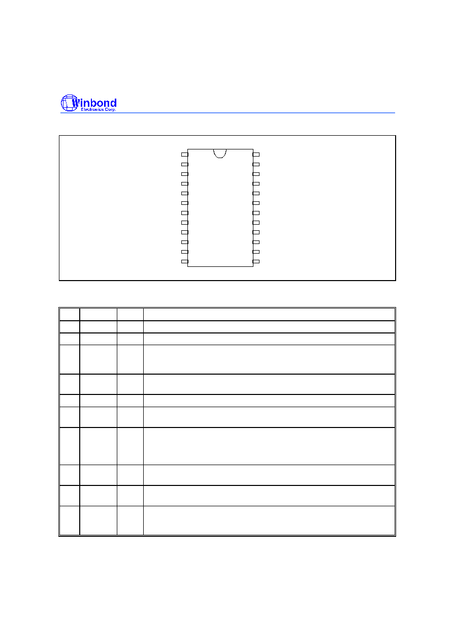
PIN CONFIGURATION
V
ALGRC
ALGR
ALGO
INTN
FCDN
FDRN
DATA
DCLK
FSKE
SLEEP/RESET
TEST2
1
2
3
4
5
6
7
8
9
10
11
12
24
23
22
21
20
19
18
17
16
15
14
13
INP
INN
GCFB
VREF
CAP
RNGDI
RNGRC
RNGON
MODE
OSCI
OSCO
V
Top View
DD
SS
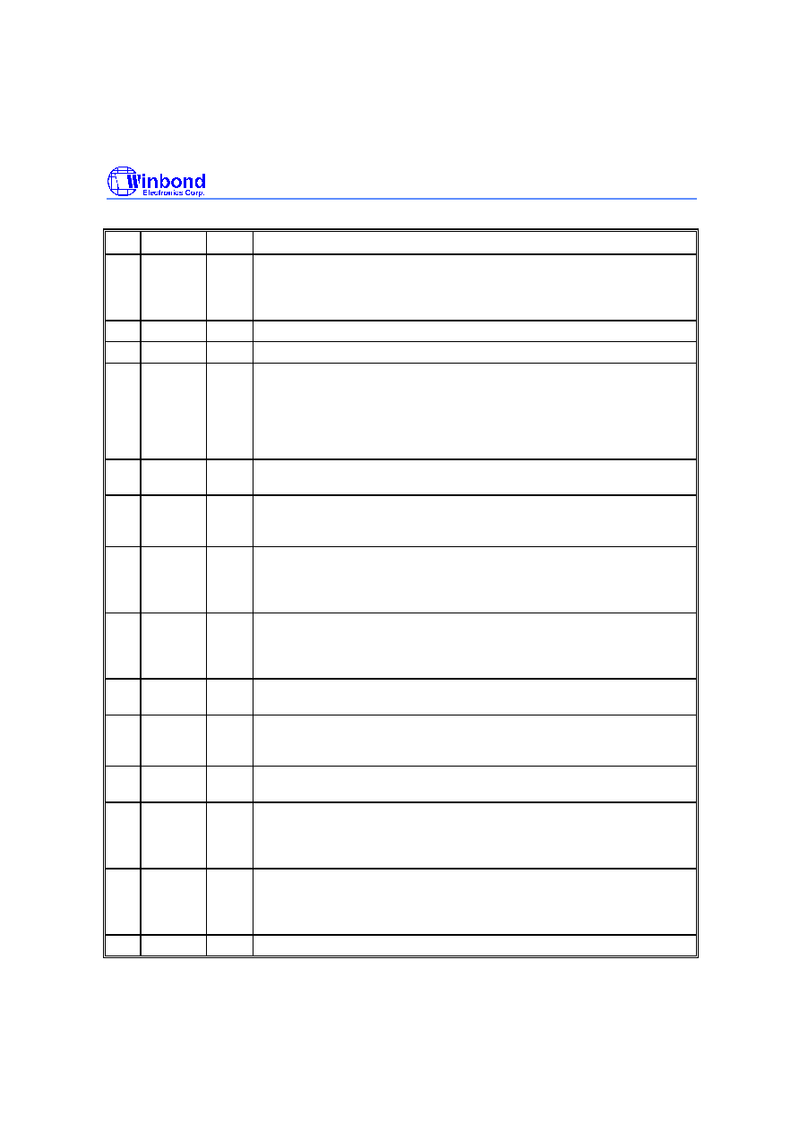
PIN DESCRIPTION
PIN NAME TYPE
DESCRIPTION
1
INP
I
Non-inverting Input of the gain control op-amp.
2
INN
I
Inverting Input of the gain control op-amp.
3
GCFB
O
Op-amp Feed-back Gain Control signal. Select the input gain by
connecting this pin and the INN pin with a feed-back resistor. It is
recommended that the op-amp be set to unity gain.
4
VREF
O
Reference Voltage. Nominally, V
DD
/2 is used to bias the input of the gain
control op-amp.
5
CAP
O
Must be connected a 0.1
�
F capacitor to V
SS
.
6
RNGDI
I
Ring Detect Input (Schmitt trigger input). Used for ring detection and line
reversal detection. Must maintain a voltage between V
DD
and V
SS
.
7
RNGRC
O
Ring RC (Open drain output and schmitt trigger input). Used to set the time
interval from the end of RNGDI pin to the inactive condition of the RNGON
pin. An external resistor must connected to V
DD
and a capacitor connected
to V
SS
, the time interval is the RC time constant.
8
RNGON
O
Ring detection output (Low active). Indicates the detection of line reversal
and/or ringing.
9
MODE
I
FSK Data interface MODE select. Sets the FSK data output interface in
mode 0 when low, or in mode 1 when high.
10
OSCI
I
Oscillator Input. A 3.579545 MHz crystal or ceramic resonator should be
connected between this pin and the OSCO pin. May be driven by an
external clock source.
Preliminary W91030B
- 4 -
Pin Descriptions, continued
PIN NAME TYPE
DESCRIPTION
11
OSCO
O
Oscillator Output. A 3.579545 MHz crystal or ceramic resonator should be
connected between this pin and the OSCI pin. Should left open or to drive
another clocked device when an external clock is connected to the OSCI
pin.
12
V
SS
I
Power Supply Ground.
13
TEST
I
Test pin. Must be connected to V
SS
for normal operation.
14
SLEEP/
RESET
I
Reset or Sleep Input (Schmitt input). When high the device will be reseted
and enter a low power state by disabling the gain control op-amp, the
oscillator and other internal circuits. The function of RNGDI, RNGRC and
the RNGON pins are not affected when the device is in a sleep condition.
This pin must be set low for normal operation. The device must reseted by
micro controller or by external RC pulse after power on.
15
FSKE
I
FSK Enable. Must be set high when for FSK demodulation. May be set low
to disable the FSK demodulator when FSK signal is not expected.
16
DCLK
I, O Data Clock for the FSK interface. In the FSK data output interface mode 0
(MODE pin low), this pin is an output with a changing FSK frequency. In
the FSK interface mode 1, this pin is an input.
17
DATA
O
Data signal for the FSK interface. Serial data output according to the FSK
frequency input in FSK data output interface mode 0 (MODE pin low). Data
is shifted out on the rising edge of DCLK in FSK data output interface
mode 1. Both logic 1 for mark and logic 0 for space.
18
FDRN
O
Data Ready of the FSK interface (Low active). In FSK interface mode 0
(MODE pin low), this pin identifies the 8-bit data boundary on the serial
output string. In FSK interface mode 1, this pin is used to notify the micro-
controller to extract the 8-bit data (ie. 8-bit data has been ready internally).
19
FCDN
O
FSK Carrier Detect (Low active). When low, it indicates the FSK signal has
been detected.
20
INTN
O
Interrupt signal (open drain). It is used to interrupt the microcontroller when
RNGON or FDRN are low, or if ALGO is high. Remains low until all three
signals have become inactive.
21
ALGO
O
Dual tone Alert signal Guard time detect Output. When high, a guard time
qualified for the dual tone alert signal has been detected.
22
ALGR
O
Dual tone Alert signal Guard time Resistor. Also functions as a dual tone
alert signal detect output without guard time. An external resistor must
connected between this pin and ALGRC to implement guard time
detection.
23
ALGRC
I
Dual tone Alert signal Guard time RC (CMOS output and internal voltage
comparator input). An external resistor must be connected between this pin
and ALGR and an external capacitor between this pin and V
DD
to
implement guard time detection.
24
V
DD
I
Power supply input.
Preliminary W91030B
Publication Release Date: March 2000
- 5 - Revision A1
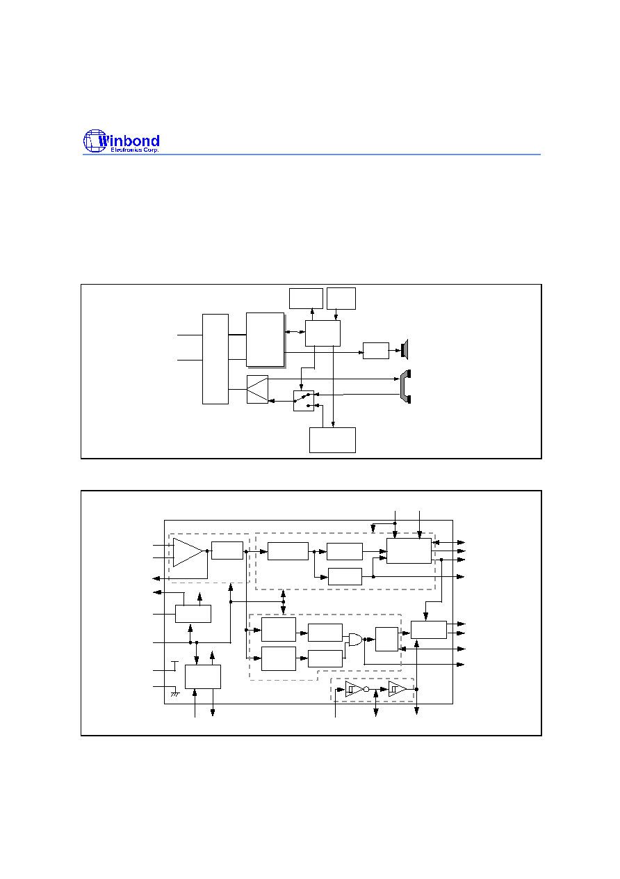
SYSTEM DIAGRAM
The W91030B device applications include telephone systems which have caller ID features and
which can display the calling message on an LCD display. Figure 5 shows the system diagram. It
illustrates how to use the chip to connect between the tip/ring and the microcontroller in the telephone
system. The ring signal is detected by the W91030B device and then an interrupt sent to the
microcontroller. The ring detected signal will also be directed to the ringer circuit. The data can be
decoded by the microcontroller and displayed on the LCD display. The DTMF ACK signal can also be
generated by the DTMF generator if a call on waiting is performed. Other functions are the same as
the telephone set.
Figure 5. System Diagram for Caller ID Application
BLOCK DIAGRAM
INP
INN
+
-
Anti-alias
Filter
FSK Bandpass
Filter
FSK
Demodulator
FSK
Data Output
Interface
FSK Carrier
Detector
High Tone
Bandpass
Filter
Low Tone
Bandpass
Filter
Guard
Time
Circuit
Bias Voltage
Generator
To internal
circuit
Oscillator
&
Clock Driver
To internal
circuit
VREF
ALGO
ALGRC
INTN
FCDN
FDRN
DATA
DCLK
SLEEP/
RESET
OSCI OSCO
RNGDI
RNGRC
RNGON
VDD
VSS
GCFB
FSKE
MODE
ALGR
Input Pre-processor
FSK Demodulation Circuit
Dual Tone Alert Signal Detection Circuit
Ring Detector
High Tone
Detector
Low Tone
Detector
Interrupt
Generator
Power down control
Power down control
CAP
Figure 6. The Block Diagram of W91030B
Micro
Controller
Handset
Speaker
Line
Interface
Winbond
Caller ID
(W91030B)
DTMF
Generator
Keypads
LCD Display
Ringer
Tip
Ring