 | –≠–ª–µ–∫—Ç—Ä–æ–Ω–Ω—ã–π –∫–æ–º–ø–æ–Ω–µ–Ω—Ç: W91590A | –°–∫–∞—á–∞—Ç—å:  PDF PDF  ZIP ZIP |
W91590 SERIES
24-MEMORY TONE/PULSE SWITCHABLE DIALER
WITH HANDFREE, HOLD AND LOCK FUNCTIONS
Publication Release Date: July 1995
- 1 -
Revision A3
GENERAL DESCRIPTION
The W91590 series dialers Si-gate CMOS IC tone/pulse switchable dialers with a 24-channel
automatic dialing memory, including a 16-digit
◊
3 emergency dialing memory, a 16-digit
◊
20
channel repertory memory that provides one-touch and three-touch dialing, and a 32-digit mercury
memory. These dialers also provide flash, clear, hold, and one-key redial functions.
FEATURES
∑
DTMF/Pulse switchable dialer
∑
32-digit LNB (last number buffer) memory (both tone and pulse mode)
∑
32-digit mercury memory (tone/pulse mode)
∑
16-digit
◊
3 one-touch direct repertory memory (tone/pulse mode)
∑
16-digit
◊
20 direct or indirect repertory memory (tone/pulse mode)
∑
Uses 9
◊
5 keyboard
∑
Flash time: 98 mS, 305 mS, or 600 mS (selectable by keypad option)
∑
Pause time: 3.6 sec.
∑
Pause P
T (pulse-to-tone) can be stored as a digit in memory
∑
Minimum tone output duration: 93 mS
∑
Minimum intertone pause: 93 mS
∑
On-chip power-on reset
∑
Uses 3.579545 MHz crystal or ceramic resonator
∑
Packaged in 22, 24 or 28-pin plastic DIP
∑
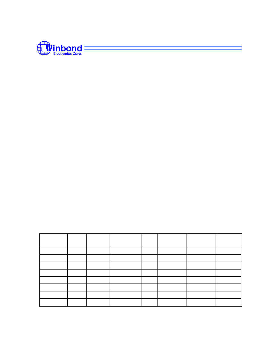
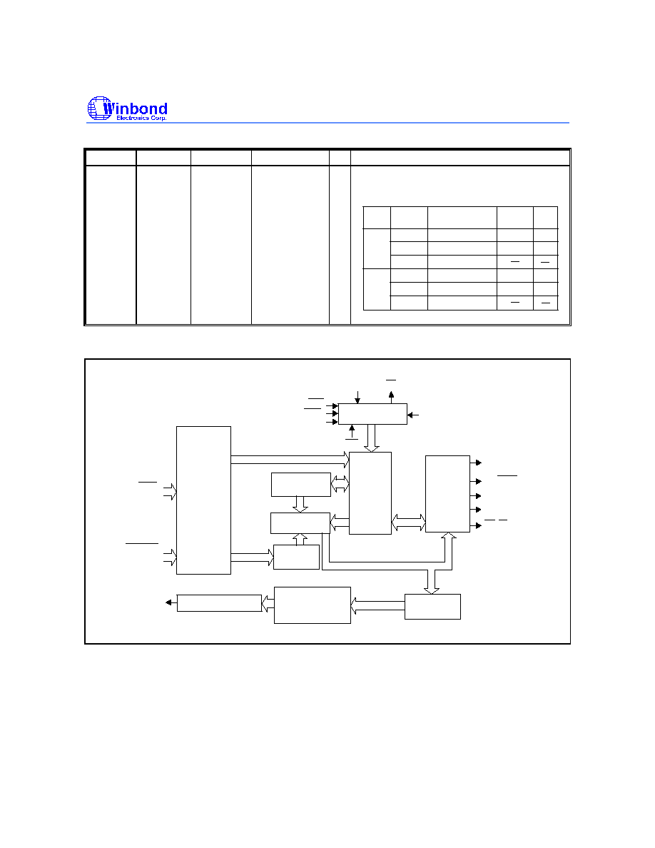
The different dialers in the W91590 series are shown in the following table:
TYPE NO. PULSE
(ppS)
MEMORY
MERCURY
MEMORY
HOLD HANDFREE
LOCK
FUNCTION
PACKAGE
W91590
10
20
-
-
-
-
22
W91590L
10
20
-
-
-
Yes
22
W91590A
10
20
-
-
Yes
-
24
W91590AL
10
20
-
-
Yes
Yes
24
W91590B
10/20
24
Yes
Yes
Yes
-
28
W91590BL
10/20
24
Yes
Yes
Yes
Yes
28
W91590C
10/20
24
Save Memory
Yes
Yes
-
28
W91590CL
10/20
24
Save Memory
Yes
Yes
Yes
28
W91590 SERIES
- 2 -
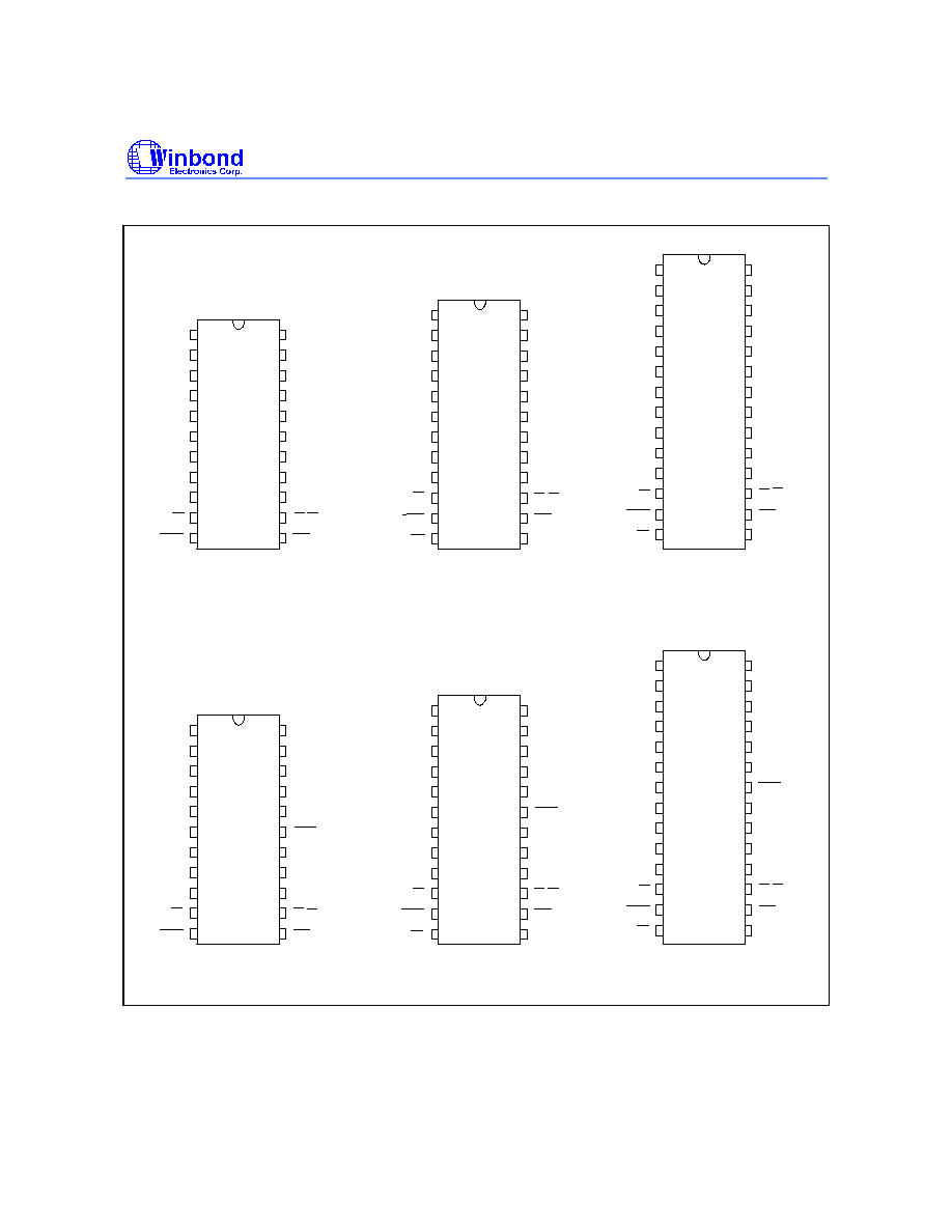
PIN CONFIGURATIONS
R2
R1
R4
1
2
3
4
5
18
19
20
21
22
C1
C3
C4
C5
C2
C6
C7
6
7
8
9
14
15
16
17
MODE
DTMF
10
11
12
13
XT
R3
V
DD
V
SS
R5
XT
T/P MUTE
HKS
DP/C9
NC
R2
R1
R4
1
2
3
4
5
20
21
22
23
24
C1
C3
C4
C5
C2
C6
C7
6
7
8
9
16
17
18
19
MODE
DTMF
10
11
12
13
14
15
XT
HFO
R3
V
DD
V
SS
R5
XT
T/P MUTE
HFI
HKS
DP/C9
NC
R2
R1
R4
1
2
3
4
5
24
25
26
27
28
C1
C3
C4
C5
C2
C6
C7
6
7
8
9
20
21
22
23
MODE
DTMF
10
11
12
17
18
19
XT
R3
V
DD
V
SS
R5
XT
DP/C9
HKS
13
14
15
16
HFO
T/P MUTE
HFI
C8
KT
DRS
HPM MUTE
NC
W91590
W91590A
W91590B/C
R2
R1
R4
1
2
3
4
5
18
19
20
21
22
C1
C3
C4
C5
C2
C6
C7
6
7
8
9
14
15
16
17
MODE
DTMF
10
11
12
13
XT
R3
V
DD
V
SS
R5
XT
T/P MUTE
HKS
DP/C9
LOCK
R2
R1
R4
1
2
3
4
5
20
21
22
23
24
C1
C3
C4
C5
C2
C6
C7
6
7
8
9
16
17
18
19
MODE
DTMF
10
11
12
13
14
15
XT
HFO
R3
V
DD
V
SS
R5
XT
T/P MUTE
HFI
HKS
DP/C9
LOCK
R2
R1
R4
1
2
3
4
5
24
25
26
27
28
C1
C3
C4
C5
C2
C6
C7
6
7
8
9
20
21
22
23
MODE
DTMF
10
11
12
17
18
19
XT
R3
V
DD
V
SS
R5
XT
DP/C9
HKS
13
14
15
16
HFO
T/P MUTE
HFI
C8
KT
DRS
HPM MUTE
W91590BL/CL
W91590AL
W91590L
LOCK
W91590 SERIES
Publication Release Date: July 1995
- 3 -
Revision A3
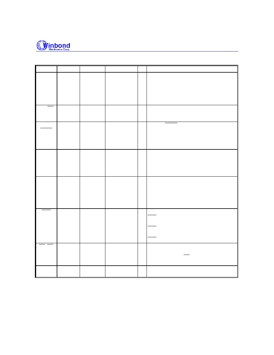
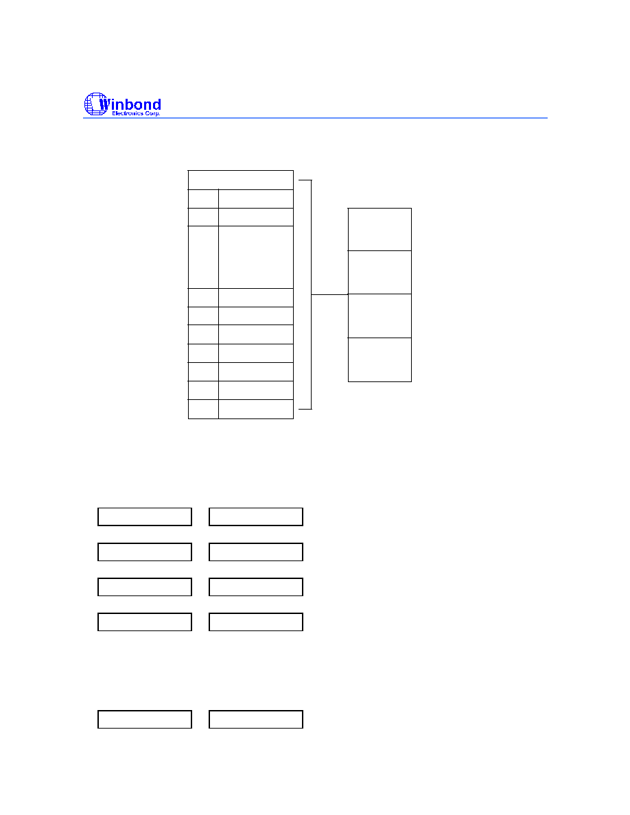
PIN DESCRIPTION
SYMBOL
22-PIN
24-PIN
28-PIN
I/O
FUNCTION
Column-
Row
Inputs
1
-
7
&
18
-
22
1
-
7
&
20
-
24
1
-
8
&
24
-
28
I
The keyboard input may be from either the
standard 9
◊
5 keyboard or an inexpensive
single contact (form A) keyboard. Electronic
input from a
µ
C can also be used.
A valid key entry is defined by a single row
being connected to a single column.
XT, XT
9, 10
9, 10
11, 12
I, O A built-in inverter provides oscillation with an
inexpensive 3.579545 MHz crystal or
ceramic resonator.
T/P
MUTE
11
11
13
O The T/P MUTE is a conventional CMOS
N-channel open drain output.
The output transistor is switched on during
pulse and tone mode dialing sequence and
flash break. Otherwise, it is switched off.
HPM
MUTE
-
-
23
O The HPM MUTE is a conventional inverter
output. During pulse dialing, flash, hold, and
mercury mute functions, this pin will output
an active high. It remains in a low state at all
other times.
MODE
15
17
19
I
Pulling mode pin to V
SS
places the dialer in
tone mode.
Pulling mode pin to V
DD
places the dialer in
pulse mode (M/B = 2:3).
Leaving mode pin floating places the dialer
in pulse mode (M/B = 1:2).
HKS
12
14
16
I
Hook switch input.
HKS = 1: On-hook state. Chip in sleeping
mode, no operation.
HKS = 0: Off-hook state. Chip enabled for
normal operation.
HKS pin is pulled to V
DD
by internal resistor.
DP /C9
13
15
17
O N-channel open drain dialing pulse output
(Figure 1).
Flash key causes DP to go active when in
pulse mode and tone mode.
NC
17
(W91590)
19
(W91590A)
22
(W91590B/C)
-
No connection.
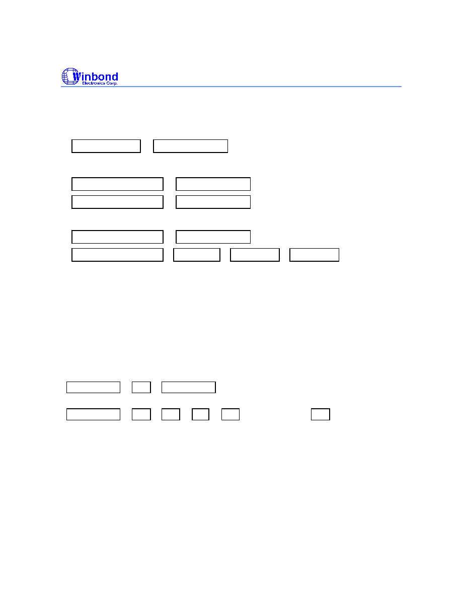
W91590 SERIES
- 4 -
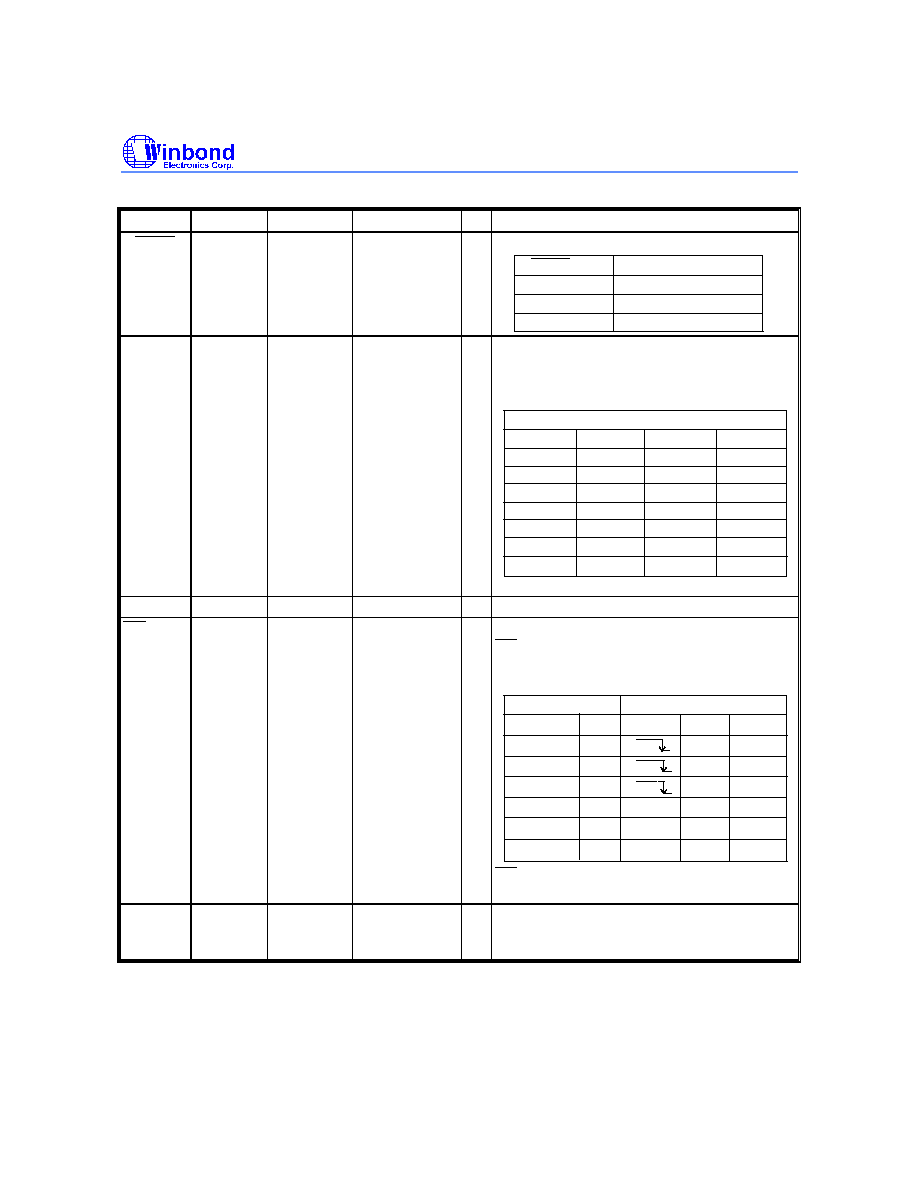
Pin Description, continued
SYMBOL
22-PIN
24-PIN
28-PIN
I/O
FUNCTION
LOCK
17
(For
W91590L)
19
(For
W91590AL)
22
(For
W91590BL/CL)
I
The function of this pin is as follows:
LOCK PIN
FUNCTION
V
DD
Floating
V
SS
"0","9" dialing inhibited
Normal dialing
"0" dialing inhibited
DTMF
14
16
18
O In pulse mode, remains in low state at all
times. In tone mode, outputs a dual or single
tone. Detailed timing diagram for tone mode
is shown in Figure 2.
OUTPUT FREQUENCY
Specified
Actual
Error%
R2
R3
R4
C1
C2
C3
697
770
852
941
1209
1336
1477
699
766
848
948
1216
1332
1472
+0.28
-0.52
-0.47
+0.74
+0.57
-0.30
-0.34
R1
V
DD,
V
SS
16, 8
18, 8
20, 10
I
Power input pins.
HFI, HFO
-
12, 13
14, 15
I, O Handfree control pins. A low pulse on the
HFI input pin toggles the handfree control
state. Status of the handfree control state is
listed in the following table:
CURRENT STATE
Hook SW.
-
On Hook
Off Hook
On Hook
Off Hook
Off Hook
HFO
Low
High
Low
High
High
-
Input
Off Hook
On Hook
On Hook
HFO
High
Low
High
Dialing
Yes
No
Yes
Yes
Yes
No
NEXT STATE
HFI
HFI
HFI
Low
Low
Low
HFI pin is pulled to V
DD
by internal resistor.
The detailed timing is shown in Fig 3.
KT
-
-
9
O Key tone signal output. A key tone will be
generated whenever a valid keys is pressed.
Frequency is 600 Hz and duration is 35 mS.
W91590 SERIES
Publication Release Date: July 1995
- 5 -
Revision A3
Pin Description, continued
SYMBOL
22-PIN
24-PIN
28-PIN
I/O
FUNCTION
DRS
-
-
21
I
Dial rate selection.
This pin is pulled to V
DD
by an internal
resistor.
DRS
MODE
PIN
TONE/PULSE
DIAL
RATE
M/B
1
2
V
DD
Floating
V
SS
V
DD
Floating
V
SS
Pulse
Pulse
Tone
Pulse
Pulse
Tone
10 ppS
10 ppS
10 ppS
20 ppS
1:2
1:2
1:2
2:3
BLOCK DIAGRAM
MODE
XT
ROW
(R1 to R5)
COLUNM
(C1 to C8)
DTMF
ROW & COLUMN
PROGRAMMABLE
COUNTER
SYSTEM CLOCK
GENERATOR
DATA LATCH
& DECODER
KEYBOARD
INTERFACE
D/A CONVERTER
XT
HKS
HFI
CONTROL
LOGIC
CONTROL
LOGIC
PULSE
LOCATION
LATCH
RAM
READ/WRITE
COUNTER
KT
HFO
DP/C9
T/P MUTE
DRS
HPM MUTE
LOCK

W91590 SERIES
- 6 -
FUNCTIONAL DESCRIPTION
Keyboard Operation
C1
C2
C3
C4
C5
C6
C7
DP /C9
C8
1
2
3
S
M00
M05
M10
M15
EM1
R1
4
5
6
MEMO
M01
M06
M11
M16
EM2
R2
7
8
9
CLR
M02
M07
M12
M17
EM3
R3
*/T
0
#
R/P
M03
M08
M13
M18
H
R4
F1
F2
F3
R
M04
M09
M14
M19
*MER
R5
MER
location in W91590C/CL is SAVE memory.
∑
S: Store function key
∑
F1, F2, F3: Flash keys
∑
R: One-key redial
∑
H: Hold function key
∑
C9 : This key is connected to pin DP /C9 via a bipolar switching transistor and a diode
∑
M0j: Direct or indirect (MEMO + M0j = M1j) repertory memory
∑
M1j: Direct repertory dialing
∑
EMi: One-touch memory for emergency call
∑
*/T: * & P
T
∑
CLR: Clear key
∑
R/P: Redial and pause function key
∑
MER: One-touch memory for mercury code dialing
∑
MEMO: Indirect repertory dialing function key
Note: Dn = 0 to 9, *, #, Mij = M00 to M19 (i = 0, 1; j = 0 to 9).
Normal Dialing
OFF HOOK
(or
ON HOOK
&
HFI
),
D1
,
D2
,
...
,
Dn
1. D1, D2, ..., Dn will be dialed out.
2. Dialing length is unlimited, but redial is inhibited if length oversteps 32 digits.
W91590 SERIES
Publication Release Date: July 1995
- 7 -
Revision A3
Redialing
1.
OFF HOOK
,
D1
,
D2
,
...
,
Dn
BUSY, Come
ON HOOK
,
OFF HOOK
(or
ON HOOK
&
HFI
),
R/P
or
ON HOOK
&
HFI
,
D1
,
D2
,
...
,
Dn
, BUSY,
HFI
Come
HFI
,
R/P
The
R/P key can execute redial function only as first key-in after off-hook. Otherwise, it will
execute pause function.
2.
OFF HOOK
(or
ON HOOK
&
HFI
),
D1
,
D2
,
...
,
Dn
,
R
a. The one-key redial function timing diagram is shown in Figure 4.
b. If dialing
of
D1
to
Dn
is completed, pressing the
R key will cause the pulse output
pin to go low for 2.2 seconds. Break time and a 600 mS pause will automatically be added.
c.
If the pulses of the dialed
number
D1
to
Dn
have not finished,
R
will be ignored.
Number Store
1.
OFF HOOK
(or
ON HOOK
&
HFI
),
S
,
D1
,
D2
,
...
,
Dn
S
,
Mij
,
EMi
or
MER
D1, D2, ..., Dn will be stored in memory location but will not be dialed out.
R/P
and
*/T
keys can be stored as a digit in memory. In store mode,
R/P
is the pause
function key.
The store mode can be released after the store function is executed or the state of the hook switch is
changed.
2.
S
,
D1
,
D2
,
...
,
Dn
,
S
,
i
,
j
D1, D2, ..., Dn will be stored in memory location Mij and will not be dialed out.
3.
S
,
D1
,
D2
,
...
,
Dn
,
S
,
MEMO
,
M0j
a. D1, D2, ..., Dn will be stored in memory location M10 to M19 and will not be dialed out.
b. MEMO + M0j = M1j.
W91590 SERIES
- 8 -
4.
OFF HOOK (or ON HOOK
&
HFI
),
D1
,
D2
,
...
,
Dn
,
S
,
S
, Mn
or
Ln
a. D1, D2, ..., Dn will be stored in memory location and will be dialed out.
b. The
S
key must be pressed after completion of the dialing sequence.
5.
D1
,
D2
,
...
,
Dn
,
S
,
S
,
i
,
j
D1, D2, ..., Dn will be stored in memory location Mij and will be dialed out.
6.
D1
,
D2
,
...
,
Dn
,
S
,
S
,
MEMO
,
M0j
a. D1, D2, ..., Dn will be stored in memory location M10 to M19 and will be dialed out.
b. MEMO + M0j = M1j.
Repertory Dialing
1.
OFF HOOK (or ON HOOK
&
HFI
),
Mij
or
EMi
or
MER
2.
OFF HOOK (or ON HOOK
&
HFI
),
MEMO
,
i
,
j
3.
OFF HOOK (or ON HOOK
&
HFI
),
MEMO
,
M0j
Access Pause
OFF HOOK
(or
ON HOOK
&
HFI
),
D1
,
D2
,
R/P
,
D3
,
...
,
Dn
1. The pause function can be stored in memory.
2. The pause function is executed in normal dialing, redialing, or memory dialing.
3. The pause function timing diagram is shown in Figure 5.
Pulse-to-Tone (*/ T)
OFF HOOK
(or
ON HOOK
&
HFI
),
D1
,
D2
,
...
,
Dn
,
*/T
,
D1'
,
D2'
,
...
,
Dn'
1. If the mode switch is set to pulse mode, then the output signal will be:
D1, D2, ..., Dn, Pause (3.6s) , D1', D2', ..., Dn'
(Pulse)
(Tone)
2. If the mode switch is set to tone mode, then the output signal will be:
D1, D2, ..., Dn, * , D1', D2', ..., Dn'
(Tone)
(Tone) (Tone)
W91590 SERIES
Publication Release Date: July 1995
- 9 -
Revision A3
3. The dialer remains in tone mode when the digits have been dialed out and can be reset to pulse
mode only by going on-hook.
4. The P
T function timing diagram is shown in Figure 6.
5. */ T key can be stored as a digit in memory
Flash (F = F1, F2, F3)
OFF HOOK
(or
ON HOOK
&
HFI
),
F
1. Flash key cannot be stored as a digit in memory, and has first priority among keyboard
functions.
2. The system will return to the initial state after the break time is finished.
3. The flash function timing diagram is shown in Figure 7.
Clear key
1.
CLR
,
R/P
(or
R
)
Redial and one-key redial buffer will be cleared.
2.
CLR
,
Mij
Location Mij buffer content will be cleared.
3.
CLR
,
i
,
j
Location Mij buffer content will be cleared.
4.
CLR
,
MEMO
,
M0j
Location Mij buffer content will be cleared.
Save
1.
OFF HOOK
(or
ON HOOK
&
HFI
), D1, D2,
...
,
Dn
S
,
S
,
SAVE
D1, D2,
...
, Dn will be stored in save memory and dialed out.
2.
OFF HOOK
(or
ON HOOK
&
HFI
),
SAVE
D1, D2,
...
, Dn will be stored in save memory but will not be dialed out.
3.
OFF HOOK
(or
ON HOOK
&
HFI
), D1, D2,
...
,
Dn
S
,
S
,
SAVE
D1, D2,
...
, Dn will be stored in save memory and dialed out.
W91590 SERIES
- 10 -
CHAIN DIALING
Relationship between the memory and the chain dialing buffer:
Memory
Digit
Location
16
M00
16
.
.
.
.
M01
.
.
.
.
.
.
M18
.
.
.
.
.
.
.
.
16
32
M19
M20
EM1
EM2
EM3
Normal Dialing
Section 1
Section 2
Section 3
Section 4
Chain Dialing Buffer
The chain dialing buffer may be divided into four sections, allowing up to four numbers to be dialed
out in sequence. For example, if the user enters M01, M03, EM1, and normal dialing (manual dialing),
the content of sections 1 to 4 will be M01, M03, EM1, and normal dialing (manual dialing). When
numbers are entered into the chain dialing buffer, there is no need to wait until the previous dialing
sequence has been completed. Numbers may be entered directly, one after the other, even while
previous numbers are being dialed out.
1.
Manual Dialing
+
Repertory Dialing
Redial buffer content = Manual dialing + Repertory dialing
2.
Repertory Dialing
+
Manual Dialing
Redial buffer content = Repertory dialing + Manual dialing
3.
Repertory Dialing
+
Repertory Dialing
Redial buffer content = Repertory dialing + Repertory dialing
4.
Redialing
+
Manual Dialing
Redial buffer content = Redialing + Manual dialing
The primary redial content may not be manual dialing, or else the last redial content will be
overwritten.
5.
Redialing
+
Repertory Dialing
W91590 SERIES
Publication Release Date: July 1995
- 11 -
Revision A3
Redial buffer content = Redialing + Repertory dialing
Redialing is valid only as the first key-in after off-hook or after the handfree dialing function is
toggled on.
The second sequence should not be performed until the first sequence is completely dialed out.
6.
Manual Dialing
+
One-Key Redialing
Redial buffer content = Manual dialing
The One-key redial may only be used after dialing out of a manual dialing sequence is completed.
7.
Repertory Dialing 1 (M1)
+
One Key Redialing
+
Repertory Dialing 2 (M2)
+
One Key Redialing
or
Repertory Dialing 1 (M1)
+
One Key Redialing
+
Repertory Dialing 2 (M2)
,
ON HOOK
,
OFF HOOK
,
Redialing
M1 and M2 represent any of the repertory dialing memories.
The first redialing will dial out M1; the second will dial out M1, M2.
If dialing out of the repertory dialing memories has not been completed, the one-key redial key will
be ignored.
Dialing of the second repertory dialing memory (M2) should not be performed until the one-key
redialing operation is completed.
Notes:
1. Chain dialing (cascaded dialing) allows for memory or manual dialing while a previous dialing sequence is still being dialed out.
2. More than one sequence of manual dialing is not permitted.
Entering more than one manual dialing sequence will inhibit redialing.
Chain dialing of more than four sections is not permitted.
Manual Dialing
+
M1
+
Manual Dialing
(two sections of manual dialing)
3. If more than four sections are entered, all sections after the fourth section will be ignored and redialing will be inhibited.
Manual Dialing
+
M1
+
M2
+
M3
+
M4
(over 4 sections, ignore
M4
and inhibit redial)
4. There is a 2.0 sec. inter-chain dialing pause for cascaded dialing.
W91590 SERIES
- 12 -
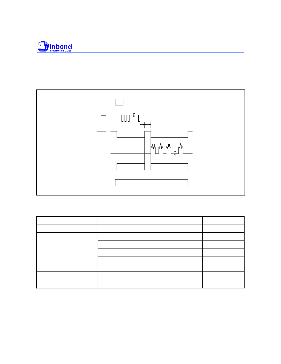
MERCURY DIALING
1. Up to 32 digits may be stored.
2. Mercury dialing is activated only as the first key-in after off-hook or handfree dialing is activated.
3. The timing diagram for the mercury memory function is given below.
T
IDP
T
P
DTMF
OSC.
KEY IN
MER
HPM MUTE
OSCILLATION
DP
T/P MUTE
Mercury Function Timing Diagram
ABSOLUTE MAXIMUM RATINGS
PARAMETER
SYMBOL
RATING
UNIT
DC Supply Voltage
V
DD
-
V
SS
-0.3 to +7.0
V
Input/Output Voltage
V
IL
V
SS
-0.3
V
V
IH
V
DD
+0.3
V
V
OL
V
SS
-0.3
V
V
OH
V
DD
+0.3
V
Power Dissipation
P
D
120
mW
Operating Temperature
T
OPR
-20 to +70
∞
C
Storage Temprature
T
STG
-55 to +125
∞
C
Note: Exposure to conditions beyond those listed under Absolute Maximum Ratings may adversely affect the life and reliability of the
device.

W91590 SERIES
Publication Release Date: July 1995
- 13 -
Revision A3
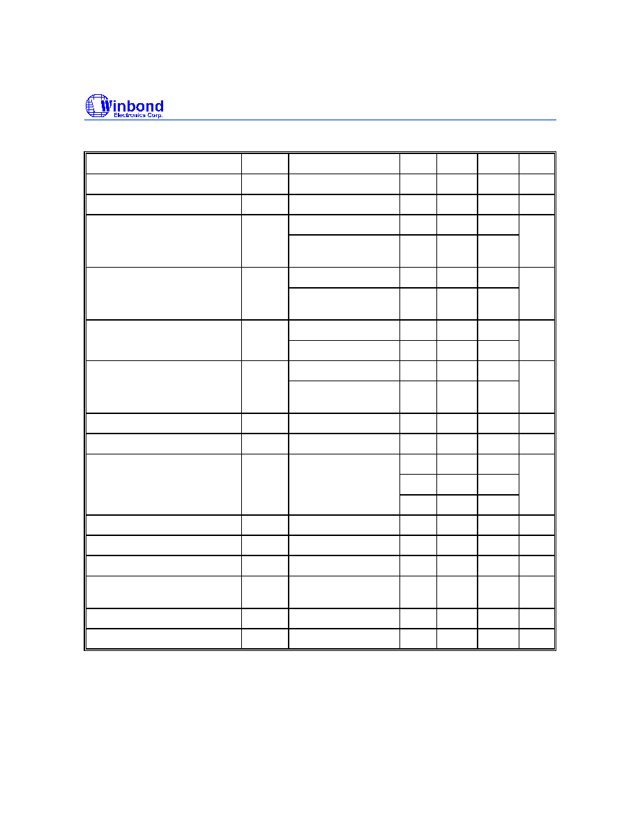
DC CHARACTERISTICS
(V
DD
-
V
SS
= 2.5V, F
OSC
. = 3.58 MHz, Ta = 25
∞
C, all outputs unloaded)
PARAMETER
SYM.
CONDITIONS
MIN. TYP.
MAX.
UNIT
Operating Voltage
V
DD
2.0
-
5.5
V
Operating Current
I
OP
Tone
-
0.3
0.5
mA
Pulse
-
0.15
0.3
Standby Current
I
SB
HKS = 0,
No load & No key entry
-
-
15
µ
A
Memory Retention Current
I
MR
HKS = 1, V
DD
= 1.0V
-
-
0.2
µ
A
DTMF Output Voltage
V
TO
Row group, R
L
= 5K
130
150
170
VrmS
Pre-emphasis
-
Col/Row, V
DD
= 2.0 to 5.5V
1
2
3
dB
DTMF Distortion
T
HD
R
L
= 5 K
, V
DD
= 2.0 to
5.5V
-
-30
-23
dB
DTMF Output DC Level
V
TDC
R
L
= 5 K
, V
DD
= 2.0 to
5.5V
1.0
-
3.0
V
DTMF Output Sink Current
I
TL
V
TO
= 0.5V
0.2
-
-
mA
DP Output Sink Current
I
PL
V
PO
= 0.5V
0.5
-
-
mA
T/P MUTE Output Sink
Current
I
ML
V
MO
= 0.5V
0.5
-
-
mA
HPM MUTE Output Sink
Current
I
HPML
V
TO
= 0.5V
0.5
-
-
mA
HPM MUTE Output drive
Current
I
HPMH
V
TH
= 2.0V
0.5
-
-
mA
HKS I/P Pull High Resistor
R
KH
-
300
500
K
Key Tone Output Current
I
KTH
V
KTH
= 2.0V
0.5
-
-
mA
I
KTL
V
KTH
= 0.5V
0.5
-
-
HFO Drive/Sink Current
I
HFH
V
HFH
= 2.0V
0.5
-
-
mA
I
HFL
V
HFL
= 0.5V
0.5
-
-
Keypad Input Drive Current
I
KD
V
I
= 0V
30
-
-
µ
A
Keypad Input Sink Current
I
KS
V
I
= 2.5V
200
400
-
µ
A
Keypad Resistance
-
-
5.0
K
W91590 SERIES
- 14 -
AC CHARACTERISTICS
PARAMETER
SYM.
CONDITIONS
MIN.
TYP.
MAX.
UNIT
Keypad Active in Debounce
T
KID
-
-
20
-
mS
Key Release Debounce
T
KRD
-
-
20
-
mS
Pre-digit Pause
1
T
PDP1
MODE Pin = 1
-
40
-
mS
10 ppS
MODE Pin =
Floating
-
33.3
-
Pre-digit Pause
2
T
PDP2
MODE Pin = 1
-
20
-
mS
20 ppS
MODE Pin =
Floating
-
16.7
-
Interdigit Pause (Auto dialing)
T
IDP
10 ppS
-
800
-
mS
20 ppS
-
500
-
Make/Break Ratio
M/B
MODE Pin = 1
-
40:60
-
%
MODE Pin =
Floating
-
33:67
-
Tone Output Duration
T
TD
Auto Dialing
-
93
-
mS
Intertone Pause
T
ITP
Auto Dialing
-
93
-
mS
Flash Break Time
T
FB
-
-
98
-
mS
-
305
-
-
600
-
Pause Time
T
P
-
-
3.6
-
S
Key Tone Frequency
F
KT
-
-
600
-
Hz
Key Tone Duration
T
KTD
-
-
35
-
mS
One-key Redialing Pause
Time
T
PR
-
-
600
-
mS
One-key Redialing Break Time
T
RB
-
-
2.2
-
S
First Key-in Pause Time
T
FKP
-
-
600
-
mS
Notes:
1. Crystal parameters suggested for proper operation are Rs < 100
, Lm = 96 mH, Cm = 0.02 pF, Cn = 5 pF, Cl = 18 pF,
F
OSC
. = 3.579545 MHz
±
0.02%.
2. Crystal oscillator accuracy directly affects these times.
W91590 SERIES
Publication Release Date: July 1995
- 15 -
Revision A3
TIMING WAVEFORMS
2
2
H
4
KEY IN
T/P MUTE
T
KID
M
B
T
PDP
DP
T
IDP
T
IDP
T
KID
T
IDP
T
PDP
LOW
KT
DTMF
OSC.
OSCILLATION
OSCILLATION
HKS
HPM MUTE
T
FKP
Figure 1. Pulse Mode Diagram (Normal Dialing)
HKS
KEY IN
T/P MUTE
T
KID
T
TD
T
ITP
DTMF
T
KRD
T
KID
T
ITP
T
ITP
T
KRD
LOW
HIGH
LOW
HPM MUTE
KT
DP
OSC.
OSCILLATION
OSCILLATION
FKP
T
Figure 2. Tone Mode Diagram (Normal Dialing)
W91590 SERIES
- 16 -
Timing Waveforms, continued
ON HOOK
HKS
OFF HOOK
HFI
HFO
LOW
HIGH
T/P MUTE
HPM MUTE
CHIP ENBLE
H KEY
Figure 3(a).
Note: The H KEY cannot be enabled when chip is disabled.
OFF HOOK
HKS
HFI
H KEY
HFO
HIGH
T/P MUTE
HPM MUTE
CHIP ENBLE
Figure 3(b).
Note: The HFI and HFI inputs will toggle the HFO signal; as soon as either HFI or H KEY is activated the HFO signal will go
high and previous inputs will be ignored.
W91590 SERIES
Publication Release Date: July 1995
- 17 -
Revision A3
Timing Waveforms, continued
ON HOOK
HKS
HFI
H KEY
HFO
HIGH
T/P MUTE
HPM MUTE
CHIP ENBLE
Figure 3(c).
Note: Changing the state of the HKS signal from high to low will initialize the HFO and HPM MUTE signals.
LOW
HKS
R
KEY IN
T/P MUTE
T
KID
DP
T
RB
T
PDP
IDP
T
T
IDP
LOW
HPM MUTE
KT
DTMF
OSC.
OSCILLATION
T
FKP
Figure 4. Pulse Mode One-key Redialing Timing Diagram (when not first key)
W91590 SERIES
- 18 -
Timing Waveforms, continued
2
R/P
2
HKS
4
KEY IN
T/P MUTE
T
KID
M
B
T
PDP
DP
T
IDP
T
IDP
B
M
T
IDP
T
PDP
T
P
LOW
HPM MUTE
KT
DTMF
OSC.
OSCILLATION
T
FKP
Figure 5. Pause Function Timing Diagram
2
*/T
8
HKS
4
KEY IN
T/P MUTE
T
KID
M
B
T
PDP
DP
T
IDP
T
IDP
B
M
T
P
T
IDP
HPM MUTE
KT
DTMF
OSC.
OSCILLATION
T
FKP
Figure 6. Pulse-to-Tone Function Timing Diagram

W91590 SERIES
Publication Release Date: July 1995
- 19 -
Revision A3
Timing Waveforms, continued
F
LOW
HKS
KEY IN
T/P MUTE
DP
T
FB
LOW
HPM MUTE
KT
DTMF
OSC.
OSCILLATION
T
FKP
Figure 7. Flash Operation Timing Diagram

W91590 SERIES
- 20 -
Headquarters
No. 4, Creation Rd. III,
Science-Based Industrial Park,
Hsinchu, Taiwan
TEL: 886-3-5770066
FAX: 886-3-5792697
http://www.winbond.com.tw/
Voice & Fax-on-demand: 886-2-7197006
Taipei Office
11F, No. 115, Sec. 3, Min-Sheng East Rd.,
Taipei, Taiwan
TEL: 886-2-7190505
FAX: 886-2-7197502
Winbond Electronics (H.K.) Ltd.
Rm. 803, World Trade Square, Tower II,
123 Hoi Bun Rd., Kwun Tong,
Kowloon, Hong Kong
TEL: 852-27516023
FAX: 852-27552064
Winbond Electronics North America Corp.
Winbond Memory Lab.
Winbond Microelectronics Corp.
Winbond Systems Lab.
2730 Orchard Parkway, San Jose,
CA 95134, U.S.A.
TEL: 1-408-9436666
FAX: 1-408-9436668
Note: All data and specifications are subject to change without notice.