
W921E880A/W921C880
4-BIT MICROCONTROLLER
Publication Release Date: July 1999
- 1 - Revision A3
Table of Contents-
1. GENERAL DESCRIPTION .........................................................................................................................3
2. FEATURES.................................................................................................................................................3
3. PIN CONFIGURATION ...............................................................................................................................6
4. PIN DESCRIPTION.....................................................................................................................................7
5. BLOCK DIAGRAM ......................................................................................................................................9
6. FUNCTIONAL DESCRIPTION .................................................................................................................10
6.1 ROM Memory Map .........................................................................................................................10
6.2 RAM Memory Map..........................................................................................................................11
6.2.1 Special Control Reg. Area..................................................................................................11
6.2.2 Stack Reg. Area.................................................................................................................12
6.2.3 Working Reg. Area ............................................................................................................12
6.3 Internal Oscillator Circuit .................................................................................................................13
6.4 Initial State ......................................................................................................................................14
6.5 Input/Output ....................................................................................................................................14
6.5.1 I/O Pull High and Open Drain Control.................................................................................17
6.6 Serial Port .......................................................................................................................................19
6.7 DTMF Generator.............................................................................................................................21
6.8 Beep Tone Generator .....................................................................................................................22
6.9 8-bit D/A Converter .........................................................................................................................23
6.10 Comparator...................................................................................................................................24
6.11 Timer 0
-
3......................................................................................................................................25
6.11.1 Arbitrary Waveform Generator.........................................................................................32
6.12 Interrupt.........................................................................................................................................33
6.12.1 Interrupt Control Register ..................................................................................................33
6.12.2 Interrupt Enable Flag........................................................................................................34
6.13 Operating Mode ............................................................................................................................34
6.14 Initial Condition Register of EPROM Program Method .................................................................39
6.15 Reset ............................................................................................................................................39

W921E880A/W921C880
- 2 -
7. ADDRESSING MODE ..............................................................................................................................40
7.1 ROM Addressing Mode ..................................................................................................................40
7.2 RAM Addressing Mode...................................................................................................................40
7.3 Look-up Table Addressing Mode (1 Word/2 Cycles) ......................................................................42
8. SPECIAL CONTROL REG. FORMAT ......................................................................................................43
9. INSTRUCTION MAP.................................................................................................................................45
10. INSTRUCTION SETS .............................................................................................................................48
11. ABSOLUTE MAXIMUM RATINGS .........................................................................................................51
12. ELECTRICAL CHARACTERISTICS.......................................................................................................52
12.1 AC Characteristics ........................................................................................................................52
12.2 DC Characteristics........................................................................................................................54
13. PACKAGE DIMENSIONS.......................................................................................................................56
80-pin QFP ............................................................................................................................................56

W921E880A/W921C880
Publication Release Date: July 1999
- 3 - Revision A3
1. GENERAL DESCRIPTION
The W921E880A/W921C880 are 4-bit micro-processor fabricated by CMOS process. With a single
channel DTMF generator, an 8-bit D/A converter circuit, a built in four by one channel comparator
circuit and four multi-function timers. The excellent memory structure, 8K super EPROM in
W921E880A and 8K mask ROM in W921C880 for program code and 1536 x 4 bit RAM minimize the
need for external memory devices. The W921E880A/W921C880 provides good solution for
consumming application, especially for telecommunication design with few external components.
Using the serial transmit/receive function, the W921E880A/W921C880 can interface with the
Winbond LCD driver IC using the serial control circuit.
2. FEATURES
Memory
�
ROM (Super EPROM): 8K
�
10 bits
�
RAM: 1536
�
4 bits
-
64
�
4 bit Special registers
-
16
�
4 bit Working registers
-
128
�
4 bit General registers
-
304
�
4 bit Multi-purpose registers4 bit serial buffer registers
-
512
�
4-bit
�
2 banks
Dual-clock Operation
�
Crystal or RC for the main system clock: RC up to 4 MHz
Crystal for 400 K, 800 K, 2 M, 3.58 M, 4 MHz
�
Crystal for subsystem clock: 32.768 KHz
I/O Pins
�
32 bidirectional and individually controllable I/O lines:
-
P0 Port: P0.0
-
P0.3 large drive current Pins
-
P1 Port: P1.0
-
P1.3 large drive current Pins
-
P2 Port: P2.0
-
P2.3 large sink current pins and open drain option
-
P3 Port: P3.0
-
P3.3 multi-function I/O
-
P4 Port: P4.0
-
P4.3 open drain and pull high resistor option, multi-function I/O
-
P5 Port: P5.0
-
P5.3 multi-function I/O
-
P6 Port: P6.0
-
P6.3 open drain and pull high resistor option, multi-function I/O
-
P7 Port: P7.0
-
P7.3 large sink current pins and open drain option
�
32 bidirectional I/O lines:
-
P8 Port: P8.0
-
P8.3 large drive current pins
-
P9 Port: P9.0
-
P9.3 large sink current pins and open drain option

W921E880A/W921C880
- 4 -
-
PA Port: PA.0
-
PA.3 open drain and pull high resistor option
-
PB Port: PB.0
-
PB.3 open drain and pull high resistor option
-
PC Port: PC.1
-
PC.3 open drain and pull high resistor option
-
PD Port: PD.0
-
PD.3 open drain and pull high resistor option
-
PE Port: PE.0
-
PE.3
-
PF Port: PF.0
-
PF.3
Interrupt
�
Four External sources: INT0 ( P4.3 )
P4 Port ( P4.0
-
P4.2 )
�
Six Internal sources: Timer 0
Timer 1
Timer 2
Timer 3
Comparator
Serial Port
Timer/Counter
�
Timer 0: 2
-
19 order divider (double source)
Auto-reload timer
Watch-dog timer
�
Timer 1: 2
-
19 order divider
Auto-reload timer
Arbitrary waveform generator
External event counter
�
Timer 2: 2
-
19 order divider
Auto-reload timer
Arbitrary waveform generator
Period/Pulse width measurement function
�
Timer 3: 2
-
19 order divider
Auto-reload timer
Operating Mode (System Clock)
�
Normal mode: System clock operating
�
HOLD mode: no operation except for oscillator (System clock stops only)
�
STOP mode: no operation including oscillator

W921E880A/W921C880
Publication Release Date: July 1999
- 5 - Revision A3
DTMF Generator and 8-bit D/A Converter
�
One Channel DTMF Generator
�
One Channel 8-bit D/A Converter
Voltage Comparator
�
Four by one Channel Voltage Comparator
Serial I/O Interface
�
Clock Synchronous multi-nibbles Serial Transmitter/Receiver Interface
Stack
�
8-bit Stack Pointer
Address Mode
�
ROM: Indirect call addressing mode
Long jump/call addressing mode
�
RAM: Direct addressing mode
Indirect addressing mode
Working reg. addressing mode
�
Look-up table addressing mode
Instruction Sets
�
117 Instruction sets
Operating Voltage
�
2.8 to 5.5V operating voltage for W921E880A EPROM Type
�
2.4 to 5.5V operating voltage for W921C880 Mask ROM Type
Package Type
�
Packaged in 80-pin QFP

W921E880A/W921C880
- 6 -
3. PIN CONFIGURATION
NC
60
PxA.3
59
PxA.2
58
PxA.1
57
N
C
T
G
F
D
6
5
6
6
6
7
6
8
7
3
7
4
7
1
7
2
6
9
7
0
7
9
8
0
7
7
7
8
7
5
7
6
B
D
T
M
P
x
C
2
P
x
C
3
P
x
C
0
P
x
F
2
P
x
F
3
P
x
F
0
P
x
F
1
P
x
E
3
V
D
P
x
E
1
P
x
E
2
P
x
E
0
P
x
C
.
.
.
.
.
.
.
.
.
.
.
.
1
3
6
3
5
3
8
3
7
4
0
3
9
3
0
2
9
3
2
3
1
3
4
3
3
2
6
2
5
2
8
2
7
X
T
N
C
N
C
/
X
T
P
x
4
1
P
x
4
0
P
x
4
3
I
N
T
0
P
x
4
.
.
.
.
2
V
S
S
N
C
P
x
7
.
1
P
x
7
.
0
P
x
7
.
3
P
x
7
.
2
P
x
5
.
1
P
x
5
.
0
T
M
2
T
M
1
/
/
/
PxD.0
PxD.1
PxD.2
PxD.3
OSCO
OSCI
V
DD
Px0.0
Px0.1
Px0.2
Px0.3
Px1.0
Px1.1
Px1.2
1
2
3
4
5
6
7
8
9
10
11
12
1
3
14
15
Px1.3
Px2.0
Px2.1
Px2.2
Px2.3
16
17
18
19
20
RESET
Px3.0/ANI0
21
22
23
24
Px3.1/ANI1
Px3.2/ANI2
Px3.3/ANI3
PxB.3
64
PxB.2
63
PxB.1
62
PxB.0
61
W921E880A
/ W921C880
PxA.0
56
Px9.3
55
Px9.2
54
Px9.1
53
Px9.0
52
Vss
51
Px6.3/RCLK
50
Px6.2/RDATA
49
Px6.1/WCLK
48
Px6.0/WDATA
47
Px8.3
46
Px8.2
45
Px8.1
44
Px8.0
43
Px5.3/DAOUT
42
Px5.2/Vref
41

W921E880A/W921C880
Publication Release Date: July 1999
- 7 - Revision A3
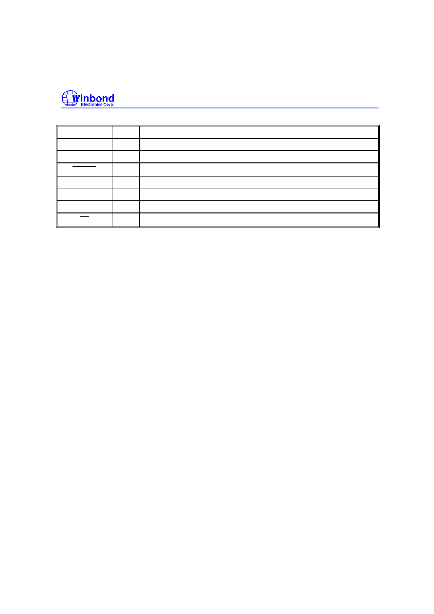
4. PIN DESCRIPTION
SYMBOL
I/O
FUNCTION
OSCI
I
Main-oscillator input pin with internal cap.
OSCO
O
Main-oscillator output pin.
PA.0
-
PA.3
*
I/O
I/O port A.
PB.0
-
PB.3
*
I/O
I/O port B.
PC.0
-
PC.3
*
I/O
I/O port C. PC.3 can be as 32.768 KHz output buffer.
PD.0
-
PD.3
*
I/O
I/O port D.
PE.0
-
PE.3
I/O
I/O port E.
PF.0
-
PF.3
I/O
I/O port F.
P0.0
-
P0.3
I/O
I/O with large drive current pin.
P1.0
-
P1.3
I/O
I/O with large drive current pin.
P2.0
-
P2.3
>
I/O
I/O with large sink current pin.
P3.0/ANI0
|
P3.3/ANI3
I/O
I/O port 3 or Analog input pins (ANI0
-
ANI3).
P4.0
*
I/O
I/O port 4.0 or the port P4.0 interrupt input pin.
P4.1
*
I/O
I/O port 4.1 or the port P4.1 interrupt input pin.
P4.2
*
I/O
I/O port 4.2 or the port P4.2 interrupt input pin.
P4.3/INT0
*
I/O
I/O port 4.3 or the INT0 input pin.
P5.0/TM1
I/O
I/O port 5.0 or the control pin of the TIMER 1.
P5.1/TM2
I/O
I/O port 5.1 or the control pin of the TIMER 2.
P5.2/VREF
I/O
I/O port 5.2 or the Vref input pin of the comparator.
P5.3/DAOUT
I/O
I/O port 5.3 or the output pin of the 8bit D/A.
P6.0/WDATA
*
I/O
I/O port 6.0 or the data output pin of the serial interface.
P6.1/WCLK
*
I/O
I/O port 6.1 or the clock I/O pin of WDATA.
P6.2/RDATA
*
I/O
I/O port 6.2 or the data input pin of the serial interface.
P6.3/RCLK
*
I/O
I/O port 6.3 or the clock I/O pin of RDATA.
P7.0
-
P7.3
>
I/O
I/O with large sink current pin.
P8.0
-
P8.3
I/O
I/O with large drive current pin.
P9.0
-
P9.3
>
I/O
I/O with large sink current pin.
W921E880A/W921C880
- 8 -
4. Pin Description, continued
SYMBOL
I/O
FUNCTION
DTMF
O
Dual tone multi-frequency output pin.
BTG
O
Beep Tone Generator output pin.
RESET
I
Reset input pin with low active.
V
DD
I
Positive power supply input pin.
V
SS
I
Negative power supply input pin.
XT
I
32.768 KHz subsystem clock input pin with internal cap.
XT
O
32.768 KHz subsystem clock output pin.
Notes:
* open drain and pull high resistor option by software
>
open drain option by software

W921E880A/W921C880
Publication Release Date: July 1999
- 9 - Revision A3
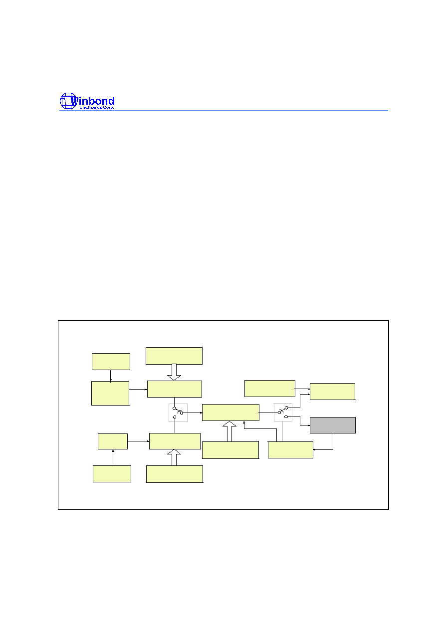
5. BLOCK DIAGRAM
PORT P1
P1.0-P1.3
PORT P2
P2.0-P2.3
PORT P3
P3.0-P3.3
PORT P4
P4.0-P4.3
PORT P5
P5.0-P5.3
PORT P6
P6.0-P6.3
PORT PA
PA.0-PA.3
PORT PB
PB.0-PB.3
PORT PC
PC.0-PC.3
A REG.
B REG.
W REG.
V REG.
U REG.
Co-V REG.
Co-U REG.
ALU
PROGRAM
COUNTER
EPROM
10 * 8K
DECODER
& CONTROL
RAM
4 * 1536
OSCILLATOR
and
SYSTEM
TIMER 0 TIMER 1 TIMER 2
DTMF GENERATOR
DTMF
+
-
STACK
POINTER
OSCI
OSCO
RESET
P5.3/DAOUT
VDD
VSS
PORT P7
P7.0-P7.3
PORT P8
P8.0-P8.3
PORT P9
P9.0-P9.3
PORT PD
PD.0-PD.3
XT
XT
PRESCALER
PORT P0
P0.0-P0.3
PORT MODE
REGISTER
PORT PE
PORT PF
PE.0-PE.3
PF.0-PF.3
TIMER 3
P3.0(ANI0)
P3.1(ANI1)
P3.2(ANI
2)
P3.3(ANI3)
D/A CONVERTOR
P5.2/VREF
DAMSB
DALSB
GENERATOR
BTG
BEEP TONE

W921E880A/W921C880
- 10 -
6. FUNCTIONAL DESCRIPTION
6.1 ROM Memory Map
Interrupt
Area
0000H
000FH
0010H
1FFFH
Indirect
Call and
Look-up
Table
Area
Long
Call/Jump
Area
0FFFH
1000H
8192 x 10-bit
0000H JMPL Instruction (RESET)
0001H XXXXX XXXXX
0002H JMPL Instruction (INT0)
0003H XXXXX XXXXX
0004H JMPL Instruction (TM 0)
0005H XXXXX XXXXX
0006H JMPL Instruction (TM1)
0007H XXXXX XXXXX
0008H JMPL Instruction (TM 2)
0009H XXXXX XXXXX
000AH JMPL Instruction (Comparator / TM 3)
000BH XXXXX XXXXX
000CH JMPL Instruction (P4.0 to P4.2 - 3 PINS)
000DH XXXXX XXXXX
000EH JMPL Instruction (SERIAL PORT)
000FH XXXXX XXXXX
PRIORITY: RESET > INT0 > TM0 > TM1 > TM2 > ( Comparator / TM3 ) > P4.0 to P4.2 > SERIAL PORT

W921E880A/W921C880
Publication Release Date: July 1999
- 11 - Revision A3
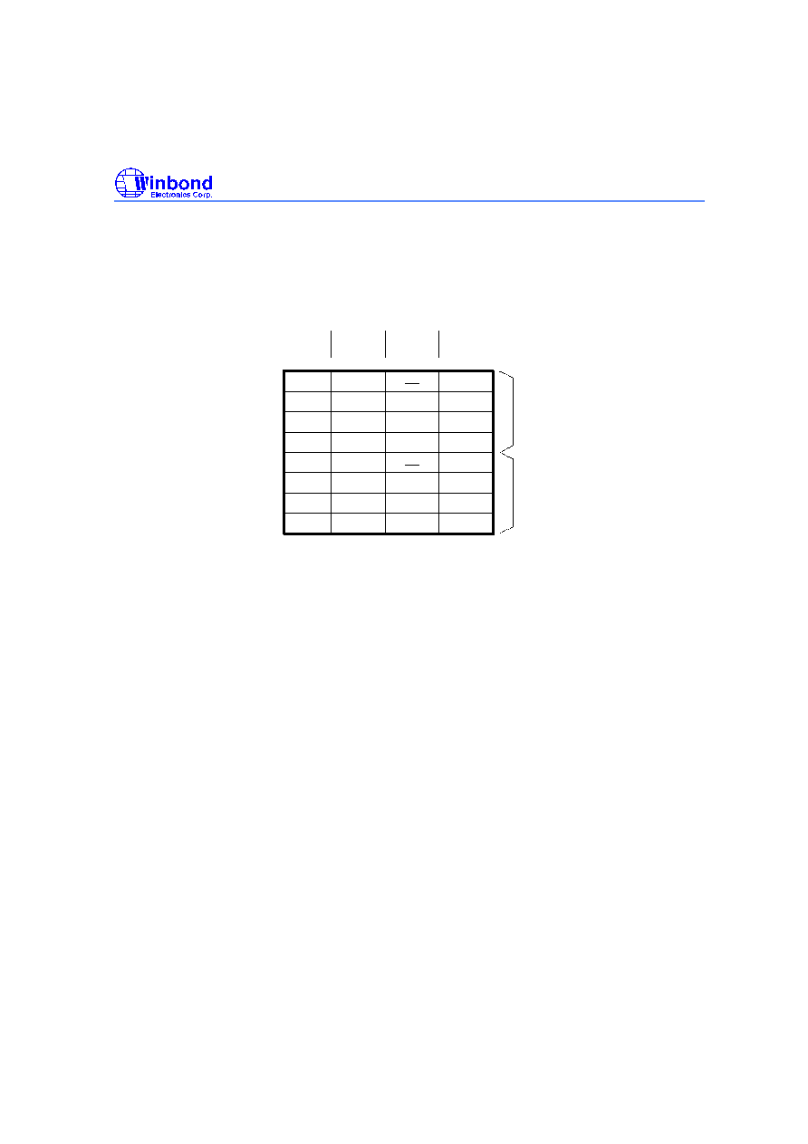
6.2 RAM Memory Map
000H
SPECIAL CONTROL REG.
SERIAL CONTROL REG.
STACK REG.
OR GENERAL REG.
OR GENERAL REG.
03FH
040H
04FH
050H
07FH
080H
0FFH
100H
17FH
180H
1FFH
000
063
064
079
080
127
128
255
256
383
384
511
WORKING REG.
200H
512
1023
3FFH
GENERAL REG.
STACK REG.
BANK0 BANK1
GENERAL REG.
SERIAL CONTROL REG.
SERIAL CONTROL REG.
(40H - FFH)
(50H - 14EH)
6.2.1 Special Control Reg. Area
There are 64 reg.
�
4 bits in the special control register area. All control registers such as the DTMF
Control Reg., System Clock Control Reg. ...etc. are in this area. Please refer to the Spesial Control
Reg. Format.
Bank Select Reg.
BKSR REG: (ADDRESS = 001H)
(Default data = 0H)
b3
b2
b1
b0
Reserved
b0
0
1
BANK NO.
0
1
b1
0
0
1
1
0
1
Reserved
Reserved
Reserved
The Bank Select Reg. can select the active bank. The memory size of each bank is 512
*4 bits. Bank 0 and bank 1 are normal
SRAM.
W921E880A/W921C880
- 12 -
6.2.2 Stack Reg. Area
There are 8 bit stack pointers in this chip located at addresses 040H
-
0FFH. After a power on reset
the stack pointer will be set to 0FFH. The stack pointer will be decreased by 4 each time a CALLP or
interrupt occurs, and will be increased by 4 each time the RTN or RTNI instruction is executed. The
format of the stack pointer is shown in the following table.
0FFH
0FEH
0FDH
0FCH
0FBH
0FAH
0F9H
0F8H
STACK 0
STACK 1
PC11
PC11
PC3
PC7
Z
PC3
PC7
Z
PC2
PC6
PC10
C
PC2
PC6
PC10
C
PC1
PC5
PC9
PC1
PC5
PC9
PC0
PC4
PC8
PC0
PC4
PC8
PC12
PC12
6.2.3 Working Reg. Area
The area located from 040H to 04FH is known as the Working Reg. The instruction MOV WRn, A or
MOV A, WRn can move the A reg. data to the Working reg. or move the Working reg. data to the A
reg. directly within 1 word/1 machine cycle. Unlike other direct instructions such as MOV Mx, A or
MOV A, Mx, these instructions use 2 words/2 machine cycles. Therefore, the Working reg. can
reduce the ROM program memory size and improve the control speed of the application circuit.
For arithmetic and logic operations only WR0
-
WR7 are available, that is only 040H to 047H can be
active.
The instructions are as follow:
ADD A, WRx
ADC A, WRx
SUB A, WRx
SBC A, WRx
ANL
A, WRx
ORL A, WRx
XRL
A, WRx
CMP A, WRx
where x = 0 -- 7.
W921E880A/W921C880
Publication Release Date: July 1999
- 13 - Revision A3
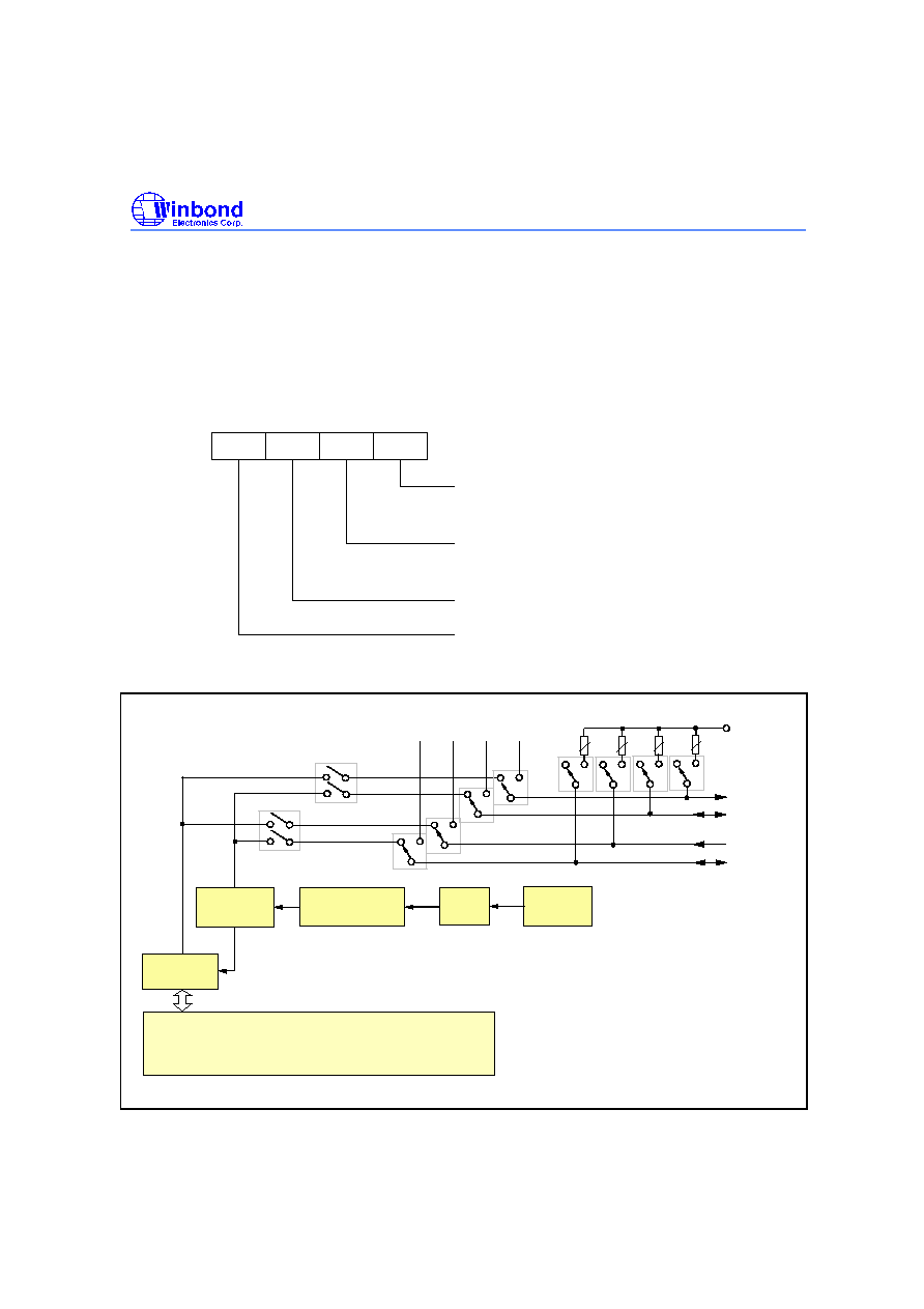
6.3 Internal Oscillator Circuit
There are dual clocks in this chip, one is a high speed clock, the other a low speed clock. The block
diagram is shown below:
TM0
TM1
TM2
TM3
MUX0
MUX3
MUX1
MUX2
f
TM0
f
TM1
f
TM2
f
TM3
Crystal Type or
RC Type
OSCI
OSCO
System Clock
(1/4)
11-bit
Prescaler
f
SYS
H
f
Crystal Type
XT
XT
1-bit
Scaler
(1/2)
2-bit Scaler
(1/4)
f
OSC
L
f
MUX0
5-bit
Prescaler
f
SYS0
f
SYS1
1
f
2
f
SYSCCR.3
SYSCCR.0
Enable
Enable
(SYSCCR.1)
(SYSCCR.2)
*
* Default: cystal type, f
1
=f
H
, f
2
=f
L
(refer to 6.14 INI register)
The format of the system clock control reg. (SYSCCR) is shown below:
SYSCCR REG: ( ADDRESS = 000H, Default data = 0H)
b3
b2
b1
b0
0 : f = fsys0
1 : f = fsys1
0 : fosc = f
1 : fosc = f
0 : f enable
1 : f disable
0 : f enable
1 : f disable
TM0
TM0
H
H
L
L
2
1
The W921E880A/W921C880 provides a crystal or RC oscillation circuit selected by bit0 of the INI
register (refer to 6.14 INITIAL CONDITION Section) to generate the system clock through external
connections. If a crystal oscillator is used, a crystal or ceramic resonator must be connected to OSCI
and OSCO , and the capacitor must be connected if an accurate frequency is needed. The oscillator
configuration is shown as follows.
OSCI
OSCO
or
OSCI
OSCO
RC Type
Crystal Type
W921E880A/W921C880
- 14 -
6.4 Initial State
The W921E880A/W921C880 is reset either by power-on reset or by using the external RESET pin.
The initial state of the W921E880A/W921C880 after the reset function is executed is described
below. The EVF interrupt request signal register value is random, so user must do CLR EVF,
#11111111b instruction to clear all interrupt request signals after power-on reset.
Program counter (PC)
0000H
Stack pointer
0FFH
Special function registers
Refer to special control register table
TM0, TM1, TM2, TM3 input clock
F
OSC/
8
TM0, TM1, TM2, TM3 contents
0FFH
Input/Output
Input mode
PM registers
1111B
DTMF output
Disable (H-Z)
EVF interrupt request signal register
Random
6.5 Input/Output
There are 64 I/O pins (4 pins
�
16 ports) including 12 large drive current pins, and 12 large sink
current pins in this chip. All the I/O pins will remain in an input mode after a power on reset.
The input or output status of port 0 to port 7 can be controlled by the port mode register PMx, where x
= 0 to 7. A zero indicates the corresponding pin is an output, a one indicates the relative pin is an
input. For example, MOV PM0, #0101B sets P0.0 and P0.2 as inputs and P0.1 and P0.3 as outputs.
The I/O instructions cannot affect the I/O status in Port 0 to Port 7.
The input or output mode of port 8 to port F only can be decided by I/O instructions. For example,
MOV A, Px will change Px to input mode and MOV Px, A will change it to output mode.
The I/O instructions are described as follows:
MOV
A, Px input Port x to A reg.
MOV
B, Px input Port x to B reg.
MOV
Px, A output A reg. data to Port x.
MOV
Px, B output B reg. data to Port x.
* P0.0
-
P0.3: Four 10 mA drive current pins
Normal I/O pins only.
* P1.0
-
P1.3: Four 10 mA drive current pins
Normal I/O pins only.
Normal function is the same as port P0
* P2.0
-
P2.3: Four 15 mA sink current pins
Normal I/O pins only.
Normal function is the same as port P0

W921E880A/W921C880
Publication Release Date: July 1999
- 15 - Revision A3
* P7.0
-
P7.3: Four 15 mA sink current pins
Normal I/O pins only.
Normal function is the same as port P0
* P3.0
-
P3.3: Multi-function I/O pins.
Normal function is the same as port P0
Special function input pins
P3IO REG: (ADDRESS = 00FH)
(Default data = 0H)
b3
b2
b1
b0
0:
1:
0:
1:
0:
1:
0:
1:
Normal I/O P3.0
Analog input pin 0 -- ANI0
Normal I/O P3.1
Normal I/O P3.2
Normal I/O P3.3
Analog input pin 1 -- ANI1
Analog input pin 2 -- ANI2
Analog input pin 3 -- ANI3
* P4.0
-
P4.3: Multi-function I/O pins.
Normal function is the same as port P0
Special function input pins
P4IO REG: (ADDRESS = 010H)
(Default data = 0H)
b3
b2
b1
b0
0:
1:
0:
1:
0:
1:
0:
1:
Normal I/O P4.3, interrupt disable
INT0
Normal I/O P4.0, interrupt disable
Interrupt port P4.0
Normal I/O P4.1, interrupt disable
Interrupt port P4.1
Normal I/O P4.2, interrupt disable
Interrupt port P4.2
W921E880A/W921C880
- 16 -
* P5.0
-
P5.3: Multi-function I/O pins.
Normal function is the same as port P0
Special function
P5IO REG: (ADDRESS = 011H)
(Default data = 0H)
b3
b2
b1
b0
0:
1:
0:
1:
0:
1:
0:
1:
Normal I/O P5.3
Normal I/O P5.0
Normal I/O P5.1
Normal I/O P5.2
Work as the timer 1 control pin
Work as the timer 2 control pin
Work as the Vref input pin of the comparator
Work as the output pin of D/A converter
(DAOUT)
* P6.0
-
P6.3 : Multi-function I/O pins.
Normal function is the same as port P0
Special function
P6IO REG: (ADDRESS = 012H)
(Default data = 0H)
b3
b2
b1
b0
0:
1:
0:
1:
0:
1:
Normal I/O P6.0
Normal I/O P6.1
Normal I/O P6.2
Work as the data output pin of the WCLK pin
(WDATA)
Work as the clock I/O pin of the WDATA pin
(WCLK)
Work as the clock I/O pin of the RDATA pin
(RCLK)
0:
1:
Work as the data input pin of the RCLK pin
(RDATA)
Normal I/O P6.3
* P8.0
-
P8.3 : Four 10 mA drive current pins
Normal I/O pins only.
Normal function is the same as port P0
* P9.0
-
P9.3 : Four 15 mA sink current pins
Normal I/O pins only.
Normal function is the same as port P0
* PA.0
-
PA.3 : Normal I/O pins only.
Normal function is the same as port P0
* PB.0
-
PB.3 : Normal I/O pins only.

W921E880A/W921C880
Publication Release Date: July 1999
- 17 - Revision A3
Normal function is the same as port P0
* PC.0
-
PC.3: Normal I/O pins only.
Normal function is the same as port P0
* PD.0
-
PD.3: Normal I/O pins only.
Normal function is the same as port P0
* PE.0
-
PE.3: Normal I/O pins only.
Normal function is the same as port P0
* PF.0
-
PF.3: Normal I/O pins only.
Normal function is the same as port P0
6.5.1 I/O Pull High and Open Drain Control
Some of the above I/O ports can be set up with a pull-high resistor or as an open drain. The user can
program the I/O through the special register so that the I/O can have a pull-high resistor or open drain
characteristics.
All pull-high resistors in the following table are 400 K
in a 3.0 voltage test condition. After a power
on reset the following special reg. will all reset to "0000".
* P4.0
-
P4.3:
P4PH REG: (ADDRESS = 003H)
(Default data = 0H)
b3
b2
b1
b0
0:
1:
0:
1:
0:
1:
0:
1:
P4.0 without pull-high resistor
P4.0 with pull-high resistor
P4.1 without pull-high resistor
P4.1 with pull-high resistor
P4.2 without pull-high resistor
P4.2 with pull-high resistor
P4.3 without pull-high resistor
P4.3 with pull-high resistor
P4TP REG: (ADDRESS = 004H)
(Default data = 0H)
b3
b2
b1
b0
0:
1:
0:
1:
0:
1:
0:
1:
P4.0 work as CMOS type
P4.0 work as Open-drain type
P4.1 work as CMOS type
P4.1 work as Open-drain type
P4.2 work as CMOS type
P4.2 work as Open-drain type
P4.3 work as CMOS type
P4.3 work as Open-drain type
W921E880A/W921C880
- 18 -
* P6.0
-
P6.3:
P6PH REG: (ADDRESS = 005H)
(Default data = 0H)
b3
b2
b1
b0
0:
1:
0:
1:
0:
1:
0:
1:
P6.0 without pull-high resistor
P6.0 with pull-high resistor
P6.1 without pull-high resistor
P6.1 with pull-high resistor
P6.2 without pull-high resistor
P6.2 with pull-high resistor
P6.3 without pull-high resistor
P6.3 with pull-high resistor
P6TP REG: (ADDRESS = 006H)
(Default data = 0H)
b3
b2
b1
b0
0:
1:
0:
1:
0:
1:
0:
1:
P6.0 work as CMOS type
P6.0 work as Open-drain type
P6.1 work as CMOS type
P6.1 work as Open-drain type
P6.2 work as CMOS type
P6.2 work as Open-drain type
P6.3 work as CMOS type
P6.3 work as Open-drain type
* PA, PB, PC, PD:
PABCDPH REG: (ADDRESS = 007H)
(Default data = 0H)
b3
b2
b1
b0
0:
1:
0:
1:
0:
1:
0:
1:
PA(4PINS) without pull-high resistor
PA(4PINS) with pull-high resistor
PB(4PINS) without pull-high resistor
PB(4PINS) with pull-high resistor
PC(4PINS) without pull-high resistor
PC(4PINS) with pull-high resistor
PD(4PINS) without pull-high resistor
PD(4PINS) with pull-high resistor
W921E880A/W921C880
Publication Release Date: July 1999
- 19 - Revision A3
PABCDTP REG: (ADDRESS = 008H)
(Default data = 0H)
b3
b2
b1
b0
0:
1:
0:
1:
0:
1:
0:
1:
PA(4PINS) work as CMOS type
PA(4PINS) work as Open-drain type
PB(4PINS) work as CMOS type
PB(4PINS) work as Open-drain type
PC(4PINS) work as CMOS type
PC(4PINS) work as Open-drain type
PD(4PINS) work as CMOS type
PD(4PINS) work as Open-drain type
* P2, P7, P9:
P279TP REG: (ADDRESS = 00DH)
(Default data = 0H)
b3
b2
b1
b0
0:
1:
0:
1:
0:
1:
P2(4PINS) work as CMOS type
P2(4PINS) work as Open-drain type
P7(4PINS) work as CMOS type
P7(4PINS) work as Open-drain type
P9(4PINS) work as CMOS type
P9(4PINS) work as Open-drain type
0:
1:
PC.3 work as normal I/O port (CMOS type)
PC.3 work as 32.768 KHz output buffer
(Open-drain Type)
6.6 Serial Port
The W921E880A/W921C880 has a clock-synchronous serial interface which transmits or receives 8-
bit data as default. The user can program the P6IO register to select port P6 as the serial port. The
serial transmitter/receiver function can be operated with a multi-nibble function where the LSB of
every nibble is being transmitted/received first.
The serial transmitted/received data is come from or stored in the serial buffer registers (address
050H to 14EH). The number of nibbles to be transmitted/received is decided by the serial MSB nibble
register (SRMNR, address = 00AH) and the serial LSB nibble register (SRLNR, address = 009H).
SRMNR register: (address = 00AH, default data = 0H)
b3
b2
b1
b0
SRLNR register: (address = 009H, default data = 2H)
b3
b2
b1
b0
The default data in the SRMNR and SRLNR registers are 0 and 2 respectively which means the
default serial interface is used to transmit/receive 8-bit data serially. As soon as these two registers
are programmed and the instructions such as SOP or SIP are executed, the serial
transmitter/receiver multi-nibble function will be performed. The transmitted/received number will be
W921E880A/W921C880
- 20 -
automatically increased by one when each nibble is transmitted/received until the number is equal to
the value in the SRLNR, SRMNR registers. Even if the HOLD instruction is executed, the SOP or SIP
function will continue to execute until completion of the transmitter/receiver function. However,
execution of the STOP instruction will stop all serial transmitter/receiver functions.
Whether transceiver data will be latched on the rising or falling edge of the clock is determined by the
serial clock inverter control register (SRINV, address = 00CH). Before the SOP or SIP instructions
are executed the SRINV register must be set to the exact value. Once both the SRINV.3 and
SRINV.2 are clear, the serial transceiver function will be forced to reset to initial status immediately.
SRINV register: (address = 00CH, default data = 0H)
b3
b2
b1
b0
0: Serial data latch at WCLK/RCLK rising edge
(normal high)
1: Serial data latch at WCLK/RCLK falling edge
(normal low)
1: WCLK and WDATA enable
1: RCLK and RDATA enable
0: WCLK and RCLK pins work as the internal
clock output pin
1: WCLK and RCLK pins work as the external
clock input pin
0: RCLK and RDATA disable (H-Z)
0: WCLK and WDATA disable (H-Z)
The serial interface configuration is shown below:
P6IO.2
P6IO.1
P6IO.0
SRINV.2
SRINV.3
SDATA
SCLK
Serial Buffer
Registers
050H
14EH
WDATA
WCLK
RDATA
RCLK
P6.0
P6.1
P6.2
P6.3
To Port P6 Normal I/O Register
P6IO.3
To Port P6
System
Clock
1/4
Serial Clock Speed
Control Circuit
f
SYS
Serial/Parallel
I/O Buffer
Clock Source
and Latch
Control Circuit
VDD
Port P6 Pull-High Resisters
P6PH
High Speed
Clock
W921E880A/W921C880
Publication Release Date: July 1999
- 21 - Revision A3
The internal serial clock can be controlled by the serial clock speed control register (SRSPC) is
described as follows:
SRSPC register: (address = 00BH, default data = 0H)
b3
b2
b1
b0
b1 b0 Input frequency
0
0
0
1
1
0
1
1
fsys/4 Hz
fsys/8 Hz
fsys/16 Hz
b3 b2
0
0
0
0
0
0
0
0
0
1
0
1
0
1
0
1
1
0
0
0
0
1
1
0
1
1
1
1
0
0
0
0
0
1
1
0
fsys/32 Hz
fsys/64 Hz
fsys/128 Hz
fsys/256 Hz
fsys/512 Hz
fsys/1024 Hz
fsys/2048 Hz
Reserved
Normally the WCLK or RCLK pin will remain in a high state and the serial data will be latched at the
rising edge of the WCLK or RCLK signal, but the serial clock inverter control register (SRINV) will
invert the above function. In this case the WCLK or RCLK pin will remain in a low state and the serial
data will be latched at the falling edge of the the WCLK or RCLK signal.
The transmitting serial clock can come from WCLK or RCLK depending upon which one is enabled. If
the serial function is disabled, it will cause the relative pins to be in a high impedance state and it will
not affect the contents of the serial buffer registers (start at address 050H).
6.7 DTMF Generator
One channel of the dual tone multi-frequency (DTMF) generator is in this chip. The exact frequency
must be decided by the OSCCTR REG to get the exact DTMF generator.
OSCCTR REG: (ADDRESS = 013H, Default data = 0H)
b3
b2
b1
b0
Reserved.
b2
b1
b0
0
0
0
0
0
1
0
1
0
0
1
1
1
0
0
1
0
1
Osc. Selection
400 KHz
800 KHz
2 MHz
4 MHz
Reserved
3.58MHz
There are four bits in the DTMF REG; the functions are described in the following table

W921E880A/W921C880
- 22 -
DTMF REG: (ADDRESS = 014H), (Default data = 0H)
b3 b2 b1
b0
FUNCTION DESCRIPTION
X X 0 0
Col 1 ( 1209 Hz ) output
X X 0 1
Col 2 ( 1336 Hz ) output
X X 1 0
Col 3 ( 1477 Hz ) output
X X 1 1
Col 4 ( 1633 Hz ) output
0 0 X X
Row 1 ( 697 Hz ) output
0 1 X X
Row 2 ( 770 Hz ) output
1 0 X X
Row 3 ( 852 Hz ) output
1 1 X X
Row 4 ( 941 Hz ) output
Note : X --- Don't care
The output of the ROW and COL is controlled by the R/C CONTROL REG.
RCCTL REG: (ADDRESS = 015H)
(Default data = 0H)
b3
b2
b1
b0
0:
1:
0:
1:
ROW frequency disable
ROW frequency enable
COL frequency disable
COL frequency enable
0:
1:
DTMF disable (H-Z)
DTMF enable
Reserved
The following table shows the DTMF keypad and its frequency.
1
4
7
*
2
5
8
0
3
6
9
#
R1
R2
R3
R4
C1
C2
C3
A
B
C
D
C4
KEY FREQUENCY
R1
R2
R3
R4
C1
C2
C3
697 Hz
770 Hz
852 Hz
941 Hz
1209 Hz
1336 Hz
1477 Hz
C4
1633 Hz
6.8 Beep Tone Generator
There are 4 kinds of frequency outputs from the BTG pin that operate as a beep tone generator.
Control of the OSCCTR REG. (ADDR = 013H) and the BTGR REG. (ADDR = 03FH) will enable the
BTG pin to output the special frequencies -- 2 KHz, 1 KHz, 630 Hz or 520 Hz.

W921E880A/W921C880
Publication Release Date: July 1999
- 23 - Revision A3
BTGR REG: ADDRESS = 03FH)
(Default data = 0H)
b3
b2
b1
b0
0:
1:
Beep Tone Generator disable
(Keep in High state)
Beep Tone Generator enable
Reserved
b1
b0
Output-Freq.
0
0
0
1
1
0
1
1
2 KHz
1 KHz
630 Hz
520 Hz
If the Beep Tone Generator is disabled by setting the BTGR REG. bit3 to "0" or after a power on
reset, the BTG output pin will remain in a high state.
6.9 8-bit D/A Converter
The content of 8-bit D/A converter is divided into D/A MSB data register (DAMSB) and D/A LSB data
register (DALSB). The block diagram is shown below.
DAMSB 4-bit
Register
DALSB 4-bit
Register
8bit D/A Converter
ANI0
ANI1
ANI2
ANI3
ANIMUX
Register
COMPTR.2
P5.2/Vref
P5.3/DAOUT
Vneg
Vpos
Vani
Vref
COMPTR.1
Vrang = 1.5 V or (2/3)V
DD
COMPTR.3
DACTL.2
� D/A Converter Control Register:
DACTL register: (ADDRESS = 016H, Default data = 0H)
b3
b2
b1
b0
0:
1: D/A converter start
D/A converter stop
1:Vrang = 1.5V
Reserved
Reserved
0:Vrang = (2/3)VDD
W921E880A/W921C880
- 24 -
When the DACTL register bit0 is set by software, the 8-bit D/A converter starts converting. The only
way to disable the D/A converter is to reset the bit0 of the DACTL register using the software control.
The analog signal will be output to the P5.3 pin in this chip if the I/O port works as the D/A output pin.
The power source of the D/A converter can be selected from the (2/3)V
DD
or 1.5V by programming
the DACTL register bit2.
� D/A Converter LSB Data Register
DALSB register: (ADDRESS = 017H, Default data = 0H)
b3
b2
b1
b0
� D/A Converter MSB Data Register
DAMSB register: (ADDRESS = 018H, Default data = 0H)
b3
b2
b1
b0
6.10 Comparator
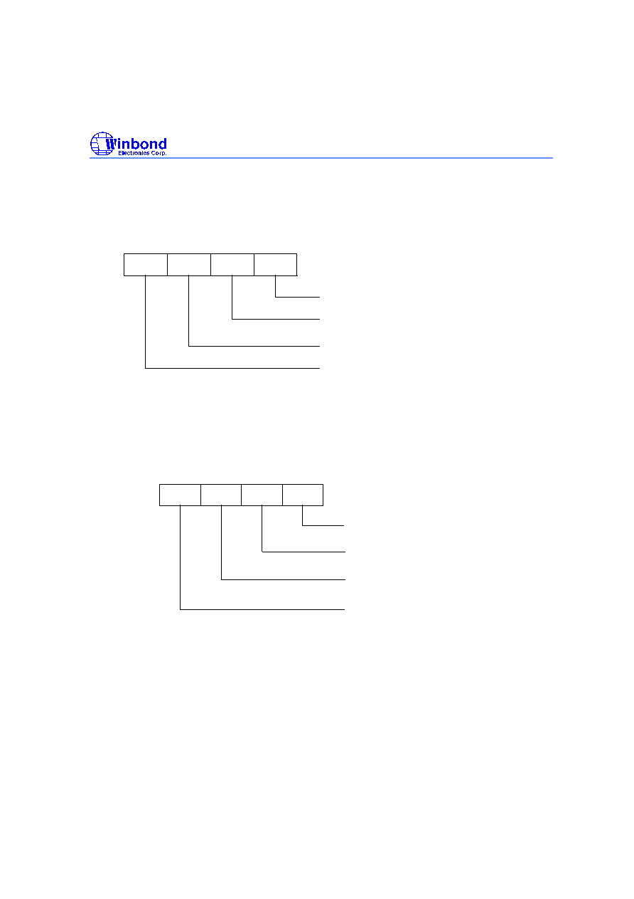
There are 4-channel inputs to the comparator negative (can be programmed to positive) terminal, but
only one channel will be active at a time. The control register is shown below.
ANIMUX register: (ADDRESS = 019H, Default data = 0H)
b3
b2
b1
b0
b0
b1
0
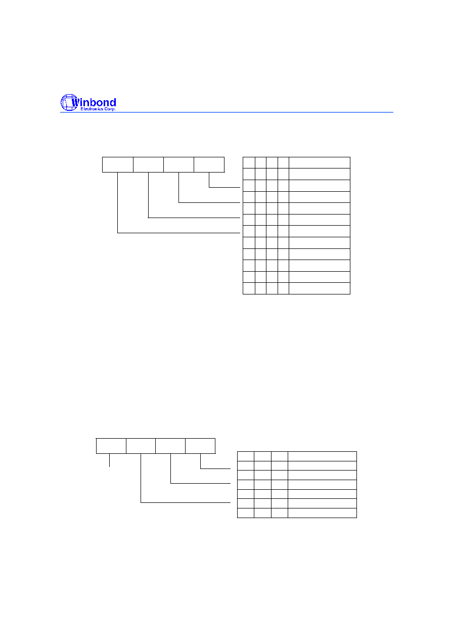
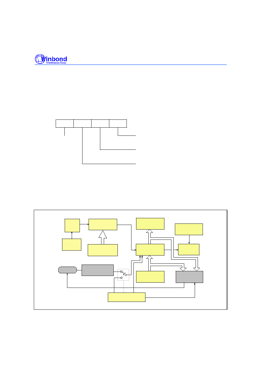
0
1
1
0
1
0
1
ANI0
Enable
ANI1
ANI2
ANI3
Reserved
Reserved
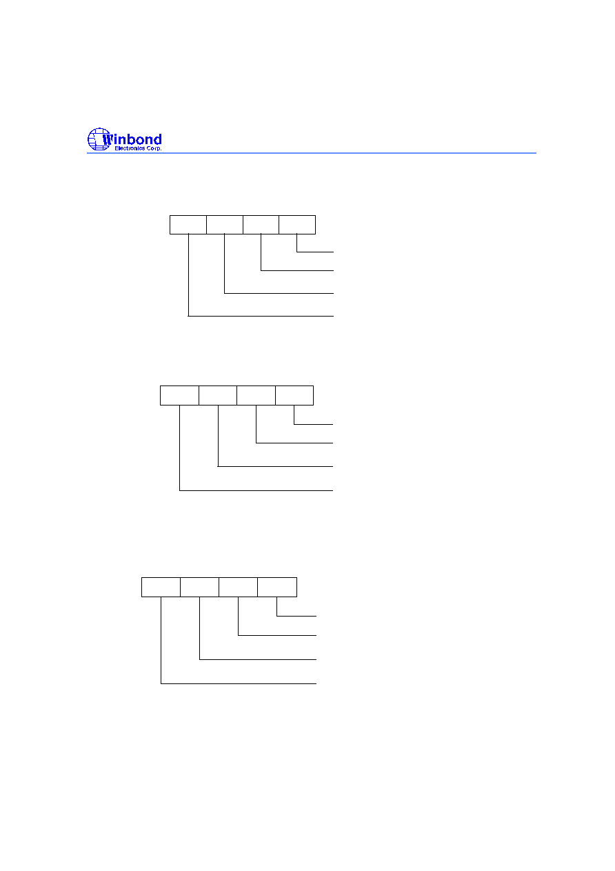
COMPTR register: (ADDRESS = 01AH, Default data = 4H)
b3
b2
b1
b0
0: Vpos voltage < Vneg voltage
1: Vpos voltage >= Vneg volatge
0: Compare stop
1: Compare start
(Read Only)
1: Vref = P5.3/DAOUT
0: Vref = P5.2/Vref
0: Vneg = Vref; Vpos = Vani
1: Vneg = Vani; Vpos = Vref
W921E880A/W921C880
Publication Release Date: July 1999
- 25 - Revision A3
When the COMPTR register bit0 is set by software, the comparator starts and the bit2 of the
COMPTR register will be set to "1" initially. The comparing result will be stored in the bit2 of the
COMPTR register and will keep this value until the bit0 of the COMPTR register is set again. The only
way to disable the comparator is to reset the bit0 of the COMPTR register using the software control.
The initial value of the COMPTR bit2 is "1", the falling edge of COMPTR bit2 will cause the
comparator interrupt to become active if the enable flag of the comparator interrupt is set.
The bit3 of the COMPTR register controls the source of Input voltage reference (Vref). The input
reference voltage (Vref) comes from external pin (P5.2/Vref) or D/A converter analog signal output
(P5.3/DAOUT).
6.11 Timer 0
-
3
There are four timers (TM0, TM1, TM2 and TM3) in this chip, and all are initialized at any time by
writing data into the TM0, TM1, TM2 and TM3 Set Reg.
TM0 can perform the following function:
1. 2
-
19 order divider
2. Auto-reload Timer
3. Watch-dog timer
TM0 Control
Register
TM0 Interrupt
Logic
Watch Dog
Timer
TM0 Control
Logic
Interrupt Control
Register
TM0 Set Register
(8 bits)
8 Order Divider
f
TM0
f
SYS1
f
SYS0
TM0 Low Speed
Register
System
Clock
1/4
f
SYS
11-bit Prescaler
5-bit Prescaler
Low Speed
Clock
1/8
f
SUB
High Speed
Clock
W921E880A/W921C880
- 26 -
The format of the Timer 0 Control Register is described as follows:
TM0CR REG: (ADDRESS = 020H)
(Default data = 0H)
b3
b2
b1
b0
b1
b0
Input frequency
0
0
0
1
1
0
1
1
fsys/2 Hz
fsys/256 Hz
fsys/1024 Hz
fsys/2048 Hz
Reserved
Reserved
(fsys0)
The format of the Timer 0 Low Speed Register is described as follows:
TM0LSR REG: (ADDRESS = 024H)
(Default data = 0H)
b3
b2
b1
b0
b1
b0
Input frequency (fsys1)
0
0
0
1
1
0
1
1
fsub/2 Hz
fsub/8 Hz
fsub/16 Hz
fsub/32 Hz
Reserved
Reserved
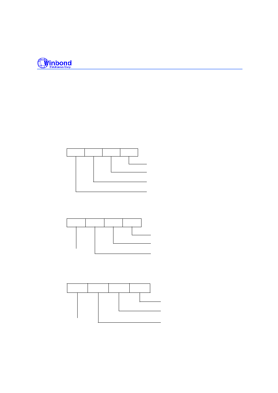
The Timer 0 Set REG. is divided into TIMER 0 MSB DATA REG.(TM0MSB REG, ADDRESS = 021H,
Default = 0FH) and TIMER 0 LSB DATA REG.(TM0LSB REG, ADDRESS = 022H, Default = 0FH).
Timer 0 will underflow when Timer 0 Set REG. goes from 00H to 0FFH. The value in the TM0MSB
and TM0LSB will be auto reloaded to the Timer 0 Set REG. when the STTM0 bit2 is set. Timer 0 will
decrease by 1 continuously during each clock transition after the timer has started.
At any time, if the STTM0 bit3 goes from 0 to 1 (disable to enable) in the timer mode, the TM0MSB
and TM0LSB will be auto reloaded to the Timer 0 Set Reg. again and the Timer 0 is restarted. Timer
0 will stop operating while the STTM0 bit3 is reset to 0.
The Timer 0 starts to count when the STTM0 REG. bit3 is set. When Timer 0 underflows, the STTM0
bit3 will be reset by hardware to stop Timer 0 if the auto-reload is disabled, but the STTM0 bit3 will
not be reset if the auto-reload is enabled.
When the Timer 0 function is performed, the watch-dog timer function will be disabled automatically.

W921E880A/W921C880
Publication Release Date: July 1999
- 27 - Revision A3
The format of the Status of Timer 0 Register is shown as follows:
STTM0 REG: (ADDRESS = 023H)
(Default data = 0H)
b3
b2
b1
b0
0:Timer 0 stop
1:Timer 0 start
0:Timer 0 normal function select
1:Watch-dog timer select
0:WDT not underflow
1:WDT underflow
0:Timer 0 auto-reload disable
1:Timer 0 auto-reload enable
If Timer 0 works as a Watch Dog Timer, then bit1 of the STTM0 REG will be set when WDT
underflows. Meanwhile, the system is reset just as in a power on reset except for the STTM0 bit1. The
WDT (STTM0 bit1) will only be reset to zero during a power on reset or during the RAM write mode.
In the timer mode or event counter mode a time out will be the programming data subtract 1
([TM0MSB,TM0LSB]-1). It is the same for timers TM1, TM2 and TM3.
TM1 can perform the following functions:
1. 2
-
19 order divider
2. Auto-reload timer.
3. Arbitrary waveform generator.
4. Event counter.
TM1 Interrupt
Logic
Interrupt Control
Register
TM1 Set Register
(8 bits)
8 Order Divider
System
Clock
1/4
11-bit Prescaler
TM1 Read
Register
TM1 Control Logic
Arbitrary
Waveform
Generator
TM1 Control
Register
f
TM1
f
SYS
Port 5.0
Event
Counter
Logic
2
High Speed
Clock

W921E880A/W921C880
- 28 -
The format of the Timer 1 Control Register is shown as follows:
TM1CR REG: (ADDRESS = 025H)
(Default data = 0H)
b3
b2
b1
b0
b1 b0
Input frequency (fsys0)
0
0
0
1
1
0
1
1
fsys/2 Hz
fsys/4 Hz
fsys/8 Hz
fsys/16 Hz
b3 b2
0
0
0
0
0
0
0
0
0
1
0
1
0
1
0
1
1
0
0
0
0
1
1
0
1
1
1
1
0
0
0
0
0
1
1
0
fsys/32 Hz
fsys/64 Hz
fsys/128 Hz
fsys/256 Hz
fsys/512 Hz
fsys/1024 Hz
fsys/2048 Hz
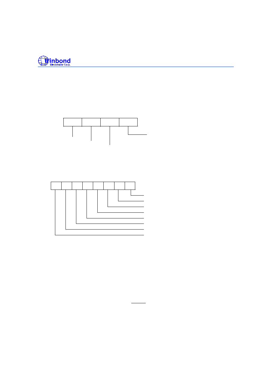
The Timer 1 Set REG. is divided into TIMER 1 MSB DATA REG.(TM1MSB REG, ADDRESS = 026H,
Default = 0FH) and TIMER 1 LSB DATA REG. (TM1LSB REG, ADDRESS = 027H, Default = 0FH).
The Timer 1 READ REG. is divided into TIMER 1 READ ONLY MSB DATA REG. (TM1RM REG,
ADDRESS = 01CH, Default = 0FH) and TIMER 1 READ ONLY LSB DATA REG. (TM1RL REG,
ADDRESS = 01DH, Default = 0FH).
The format of the Status of Timer 1 Register is shown as follows:
STTM1 REG: (ADDRESS = 028H)
(Default data = 0H)
b3
b2
b1
b0
0:Timer 1 stop
1:Timer 1 start
0:
1:
Timer 1 normal function select
Special function select
Reserved
0:Timer 1 auto-reload disable
1:Timer 1 auto-reload enable
If Timer 1 is in the timer mode, the Timer 1 will underflow when it goes from 00H to 0FFH. The value
in the TM1MSB and TM1LSB will be auto reloaded to the Timer 1 Set REG. when the STTM1 bit2 is
set. Timer 1 will decrease by 1 continuously at each clock transition after the timer has started.
At any time the STTM1 bit3 goes from 0 to 1 (disable to enable), the TM1MSB and TM1LSB will be
auto reloaded to the Timer 1 Set Reg. again and Timer 1 is restarted. Timer 1 will stop operating
while the STTM1 bit3 is reset to 0.
W921E880A/W921C880
Publication Release Date: July 1999
- 29 - Revision A3
The Timer 1 starts to count when the STTM1 REG. bit3 is set. When Timer 1 underflows, the STTM1
bit3 will be reset by hardware to stop Timer 1 if the auto-reload is disabled, but the STTM1 bit3 will
not be reset if the auto-reload is enabled.
When the Timer 1 function is performed, the special function will be disabled automatically. The
special function input or output is from or to P5.0.
The format of the Timer 1 event counter condition is shown as follows
TGTM1 REG: (ADDRESS = 029H)
(Default data = 0H)
b3
b2
b1
b0
0: Event counter is falling edge trigger
1: Event counter is rising edge trigger
0: Special function work as event counter
1: Special function work as arbitrary
waveform generator
0: Arbitrary waveform type 0
1: Arbitrary waveform type 1
Reserved
TM2 can perform the following functions:
1. 2
-
19 order divider
2. Auto-reload timer.
3. Arbitrary waveform generator.
4. Pulse/Period width measurement function
Period/Pulse Width
Measurement
TM2 Interrupt
Logic
Interrupt Control
Register
TM2 Set Register
(8 bits)
8 Order Divider
System
Clock
1/4
11-bit Prescaler
TM2 Read
Register
Arbitrary
Waveform
Generator
TM2 Control
Register
f
TM2
f
SYS
Port 5.1
TM2 Control Logic
High Speed
Clock

W921E880A/W921C880
- 30 -
TM2CR REG: (ADDRESS = 02AH)
(Default data = 0H)
b3
b2
b1
b0
b1 b0
Input frequency (fTM2)
0
0
0
1
1
0
1
1
fsys/2 Hz
fsys/4 Hz
fsys/8 Hz
fsys/16 Hz
b3 b2
0
0
0
0
0
0
0
0
0
1
0
1
0
1
0
1
1
0
0
0
0
1
1
0
1
1
1
1
0
0
0
0
0
1
1
0
fsys/32 Hz
fsys/64 Hz
fsys/128 Hz
fsys/256 Hz
fsys/512 Hz
fsys/1024 Hz
fsys/2048 Hz
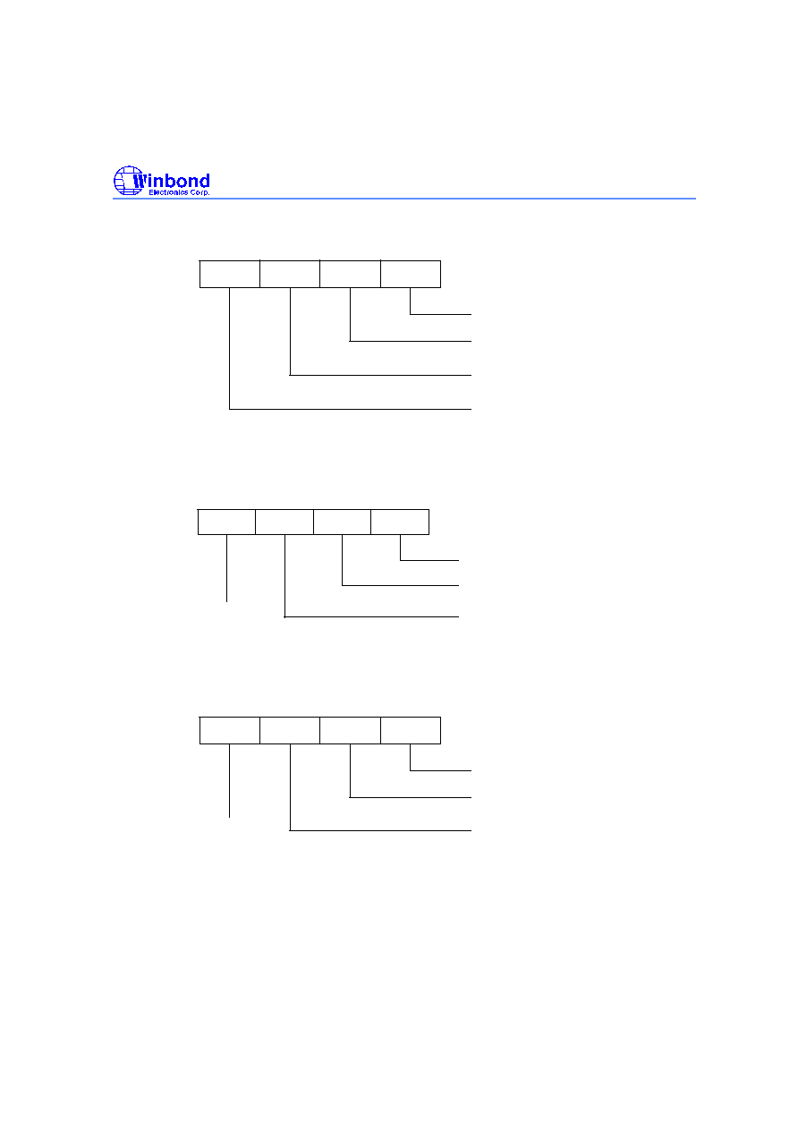
The Timer 2 Set REG. is divided into TIMER 2 MSB DATA REG. (TM2MSB REG, ADDRESS =
02BH, Default = 0FH) and TIMER 2 LSB DATA REG. (TM2LSB REG, ADDRESS = 02CH, Default =
0FH).
The Timer 2 READ REG. is divided into TIMER 2 READ ONLY MSB DATA REG. (TM2RM REG,
ADDRESS = 01EH, Default = 0FH) and TIMER 2 READ ONLY LSB DATA REG. (TM2RL REG,
ADDRESS = 01FH, Default = 0FH).
The format of the Status of Timer 2 Register is shown as follows:
STTM2 REG: (ADDRESS = 02DH)
(Default data = 0H)
b3
b2
b1
b0
0:Timer 2 stop
1:Timer 2 start
0:
1:
Timer 2 mormal function select
Special function select
0:Timer 2 auto-reload disable
1:Timer 2 auto-reload enable
Reserved
If Timer 2 is in the timer mode, the Timer 2 will underflow when it goes from 00H to FFH. The value
in TM2MSB and TM2LSB will be auto reloaded to the Timer 2 Set REG. Timer 2 will decrease by 1
continuously at each clock transition after the timer has started.
At any time the STTM2 bit3 goes from 0 to 1 (disable to enable), TM2MSB and TM2LSB will be auto
reloaded to the Timer 2 Set Reg. again and the Timer 2 is restarted. Timer 2 will stop operating when
the STTM2 bit3 is reset to 0.

W921E880A/W921C880
Publication Release Date: July 1999
- 31 - Revision A3
Timer 2 starts to count when the STTM2 REG. bit3 is set. When Timer 2 underflows, the STTM2 bit3
will be reset by hardware to stop Timer 2 if the auto-reload is disabled, but the STTM2 bit3 will not be
reset if the auto-reload is enabled.
When the Timer 2 function is performed, the special function is automatically disabled.
The format of the trigger condition of the Timer 2 Register is shown as follows:
TGTM2 REG: (ADDRESS = 02EH)
(Default data = 0H)
b3
b2
b1
b0
0: Special function work as pulse/period
width measurement
1: Special function work as arbitrary
waveform generator
0: Arbitrary waveform type 0
1: Arbitrary waveform type 1
b1
b0
0
0
0
1
1
0
1
1
Trigger
-----
Rising
Falling
Both
In pulse/period width measurement mode, the measuring-data is the 1'S complement of the exact
data and the TM2 interrupt flag is set at every 255 timer clock occurences or if the 2nd trigger
condition occurs. So the measured pulse/period width is (255(N 1) TM2) * T
- +
, where N is the
number of interrupt flag occurences,
b3
b2
b1
b0
0:
1:
0:
1:
ROW frequency disable
ROW frequency enable
COL frequency disable
COL frequency enable
0:
1:
DTMF disable (H-Z)
DTMF enable
Reserved
is the 1'S complement of timer2 register, and T is the
period of the timer 2 clock. The special function input or output is from or to P5.1.
TM3 can perform the following functions:
1. 2
-
19 order divider
2. Auto-reload timer.
System
Clock
1/4
11-bit Prescaler
TM3 Control
Register
TM3 Interrupt
Logic
TM3 Control
Logic
Interrupt Control
Register
TM3 Set Register
(8 bits)
8 Order Divider
f
TM3
f
SYS
High Speed
Clock

W921E880A/W921C880
- 32 -
TM3CR REG: (ADDRESS = 02FH)
(Default data = 0H)
b3
b2
b1
b0
b1 b0
Input frequency (fTM3)
0
0
0
1
1
0
1
1
fsys/2 Hz
fsys/4 Hz
fsys/8 Hz
fsys/16 Hz
b3 b2
0
0
0
0
0
0
0
0
0
1
0
1
0
1
0
1
1
0
0
0
0
1
1
0
1
1
1
1
0
0
0
0
0
1
1
0
fsys/32 Hz
fsys/64 Hz
fsys/128 Hz
fsys/256 Hz
fsys/512 Hz
fsys/1024 Hz
fsys/2048 Hz
The Timer 3 Set REG. is divided into TIMER 3 MSB DATA REG. (TM3MSB REG, ADDRESS =
030H, Default = 0FH) and TIMER 3 LSB DATA REG. (TM3LSB REG, ADDRESS = 031H, Default =
0FH).
The format of the Status of Timer 3 Register is shown as follows:
STTM3 REG: (ADDRESS = 032H)
(Default data = 0H)
b3
b2
b1
b0
0:Timer 3 stop
1:Timer 3 start
0:Timer 3 auto_reload disable
1:Timer 3 auto-reload enable
Reserved
Reserved
6.11.1 Arbitrary Waveform Generator
Both TM1 and TM2 have arbitrary waveform generator circuits. The following description describes
their opeation.
TYPE 0 :
256T
NT
NT
T
TYPE 1 :
N = 0 Will keep the waveform in the high state.
N = 1 Will keep the waveform in the low state.
Note: N is the value stored in the TM1 Set Reg. (TM1MSB, TM1LSB) or TM2 Set Reg. (TM2MSB, TM2LSB)
W921E880A/W921C880
Publication Release Date: July 1999
- 33 - Revision A3
6.12 Interrupt
There are 10 interrupt sources. There are four external sources: INT0 (P4.3) and P4 Port
(P4.0
-
P4.2), triggered by the falling edge signals of external sources, and six internal sources:
Timer0, Timer1, Timer2, Timer3, Comparator and Serial Port. The priority of those interrupts is INT0
> TM0 > TM1 > TM2 > ( Comparator / TM3 ) > P4.0 to P4.2 > SERIAL.
6.12.1 Interrupt Control Register
The INTERRUPT CONTROL REG.1
-
3 (INTCT1
-
INTCT3) controls which interrupt is enabled. The
formats are shown below:
INTCT1 REG: (ADDRESS = 039H)
(Default data = 0H)
b3
b2
b1
b0
0: TM0 interrupt disable
1: TM0 interrupt enable
0: TM1 interrupt disable
1: TM1 interrupt enable
0: TM2 interrupt disable
1: TM2 interrupt enable
0: TM3 interrupt disable
1: TM3 interrupt enable
INTCT2 REG: (ADDRESS = 03AH)
(Default data = 0H)
b3
b2
b1
b0
0: SERIAL interrupt disable
1: SERIAL interrupt enable
0: INT0 pin interrupt disable
1: INT0 pin interrupt enable
0: COMPARATOR interrupt disable
1: COMPARATOR interrupt enable
Reserved
INTCT3 REG: (ADDRESS = 03BH)
(Default data = 0H)
b3
b2
b1
b0
0: P4.0 PORT interrupt disable
1: P4.0 PORT interrupt enable
0: P4.1 PORT interrupt disable
1: P4.1 PORT interrupt enable
0: P4.2 PORT interrupt disable
1: P4.2 PORT interrupt enable
Reserved
W921E880A/W921C880
- 34 -
6.12.2 Interrupt Enable Flag
When the interrupt is enabled by an event, the program counter will jump to the interrupt address and
the Enable InterruptT Flag (ENINT) bit0 is cleared. All the interrupts will also be disabled at the same
time. The only method to enable the interrupt again is to set the ENINT bit0 or to execute the RTNI
instruction.
ENINT REG: (ADDRESS = 034H)
(Default data = 0H)
b3
b2
b1
b0
0: Disable all interrupt
1: Enable all interrupt
Reserved
Reserved
Reserved
When the interrupt is enabled by an event, the individual interrupt request signal is automatically
cleared by the hardware with the other interrupt request signals kept in the same condition. The only
way to reset the interrupt request signal is to execute the instruction CLR EVF, #I (I is a 8bits data, for
example, CLR EVF, #00000001b instruction implies to clear TM0 interrupt request signal). This
instruction is a 2 word / 2 cycle instruction; the format of the immediate data is shown as follows:
i3
i2
i1
i0
1: TM2 int. request signal is cleared
1: TM1 int. request signal is cleared
1: TM0 int. request signal is cleared
1: TM3 int. request signal is cleared
i4
i5
i6
i7
1: SERIAL int. request signal is cleared
1: P4 int. request signal is cleared
1: INT0 int. request signal is cleared
1: COMPARATOR int. request signal is cleared
6.13 Operating Mode
There are 3 types of operating mode, Normal Mode , Hold Mode, and Stop Mode.
6.13.1 Normal Mode
All functions operate with the
�
P functioning according to the system clock.
6.13.2 Hold Mode
The
�
P enters the HOLD MODE when the HOLD instruction is executed from NORMAL MODE. In
this mode, the system clock is stopped, so the program counter (PC) will also stop. But the oscillator,
timer/ counter, serial port and interrupt active pins continue to function.
The HOLD MODE can be released only by the RESET pin or by an interrupt request signal. When
the hold mode is released, either the hold mode is released only, or the hold mode is released and
the interrupt subroutine (interrupt vector) is serviced. The HOLD MODE RELEASES FLAG 1, 2, 3
(HMRF1, 2, 3) (ADDRESS = 036H, 037H, 038H) which can control the flow. The formats of these
three flags are shown below.

W921E880A/W921C880
Publication Release Date: July 1999
- 35 - Revision A3
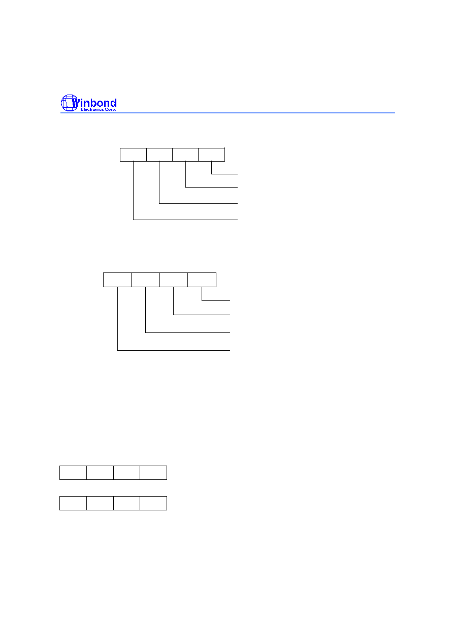
HMRF1 REG: (ADDRESS = 036H)
(Default data = 0H)
DAMSB 4-bit
Register
DALSB 4-bit
Register
8bit D/A Converter
ANI0
ANI1
ANI2
ANI3
ANIMUX
Register
COMPTR.2
P5.2/Vref
P5.3/DAOUT
Vneg
Vpos
Vani
Vref
COMPTR.1
Vrang = 1.5 V or (2/3)V
DD
COMPTR.3
DACTL.2
HMRF2 REG: (ADDRESS = 037H)
(Default data = 0H)
b3
b2
b1
b0
0: Special function work as pulse/period
width measurement
1: Special function work as arbitrary
waveform generator
0: Arbitrary waveform type 0
1: Arbitrary waveform type 1
b1
b0
0
0
0
1
1
0
1
1
Trigger
-----
Rising
Falling
Both
HMRF3 REG: (ADDRESS = 038H)
(Default data = 0H)
b3
b2
b1
b0
0: P4.1 PORT hold released disable
1: P4.1 PORT hold released enable
0: P4.2 PORT hold released disable
1: P4.2 PORT hold released enable
0: P4.0 PORT hold released disable
1: P4.0 PORT hold released enable
Reserved
The HOLD RELEASED STATUS FLAG 1, 2, 3 (HRSTS1, 2, 3) (ADDRESS = 03CH, 03DH, 03EH)
stores the information that caused the HOLD MODE to be released. The format is shown below.
W921E880A/W921C880
- 36 -
HRSTS1 REG: (ADDRESS = 03CH) (Read Only)
(Default data = 0H)
b3
b2
b1
b0
1: HOLD has released by TM0
1: HOLD has released by TM1
1: HOLD has released by TM2
1: HOLD has released by TM3
HRSTS2 REG: (ADDRESS = 03DH) (Read Only)
(Default data = 0H)
b3
b2
b1
b0
1: HOLD has released by the INT0 pin
1: HOLD has released by SERIAL Port
1: HOLD has released by COMPARATOR
Reserved
HRSTS3 REG: (ADDRESS = 03EH) (Read Only)
(Default data = 0H)
b3
b2
b1
b0
1: HOLD has released by P4.0
1: HOLD has released by P4.1
1: HOLD has released by P4.2
Reserved
HRSTS1, 2, and 3 are read only registers and cleared by the instruction CLR EVF #I.
W921E880A/W921C880
Publication Release Date: July 1999
- 37 - Revision A3
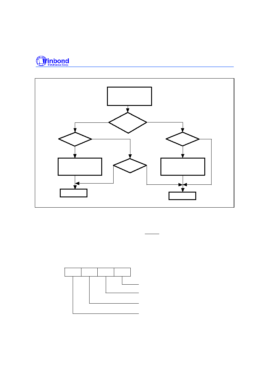
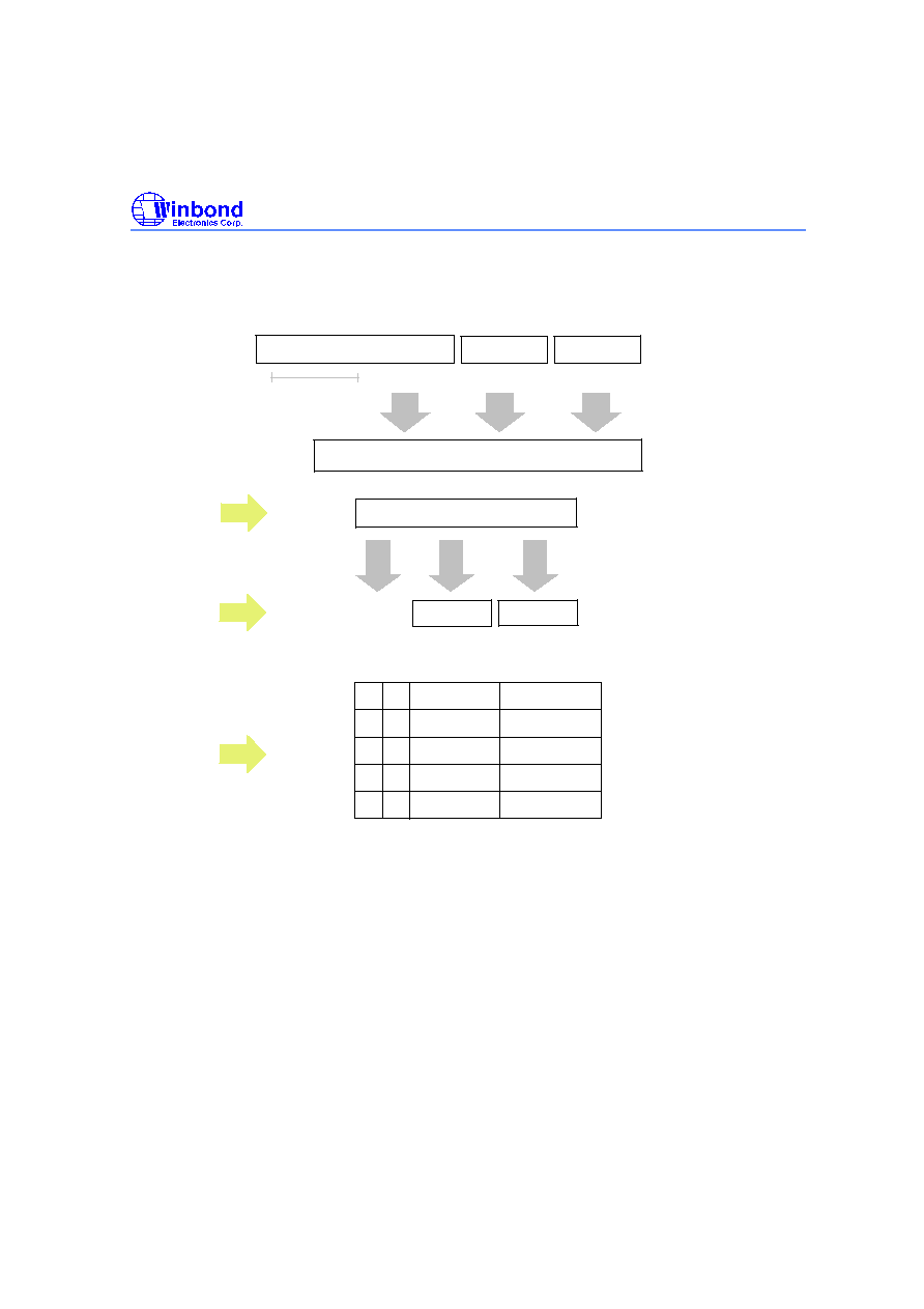
Hold Mode Operation Flow Chart
In
HOLD
Mode ?
Flag Set?
PC <- (PC+1)
No
Yes
No
Yes
Yes
No
Yes
No
HOLD
HMRF
Flag Set?
Execute
Interrupt Service Routine
Interrupt
Flag Set?
Interrupt
Hold Release
Reset ENINT Flag and
individual Request
Flag
Execute
Interrupt Service Routine
Reset ENINT Flag and
individual Request Flag
TM0 to TM3 Serial;
occurs at INT0, P4.0-P4.2
Comparator; Falling change
INTCT
INTCT
6.13.3 Stop Mode
The
�
P enters the STOP MODE only if the stop instruction is executed. All chip functions are
disabled because both of the oscillators are stopped.
The stop mode can be released by the low level of the RESET pin, INT0 pin, P4 port, PA port or PB
port. The STOP CONDITION RELEASE FLAG (STPRF ADDRESSS = 035H) is the STOP mode
release control reg.
STPRF REG.: (ADDRESS = 035H)
(Default data = 8H)
b3
b2
b1
b0
0:
1:
0:
1:
Stop released by INT0 (P4.3) is disable
0:
1:
0:
1: Stop released by INT0 (P4.3) is enable
Stop released by any pin of PB is disable
Stop released by any pin of PB is enable
Stop released by any pin of P4.0-P4.2 is disable
Stop released by any pin of P4.0-P4.2 is enable
Stop released by any pin of PA is disable
Stop released by any pin of PA is enable
W921E880A/W921C880
- 38 -
When the STOP CONDITION RELEASE FLAG (STPRF) and the INTERRUPT CONTROL REG.
(INTCT1
-
INTCT3) are set before the STOP instruction is executed, a low level signal on the P4, PA
or PB ports will cause the STOP MODE to be released. There will be a delay of about 256 machine
cycles after the stop mode is released. The interrupt subroutine (interrupt vector) is then executed
according to the set bit in the STPRF REG. If the interrupt enable flag is not set before the STOP
instruction is executed, then the next instruction after the STOP instruction will be executed. It also
has a delay of about 256 machine cycles before the next instruction is executed.
It should be noted that if STOP MODE is released by the PA or PB port, then the chip will execute the
(PC+1) instruction only because there is no individual interrupt subroutine in the PA and PB ports.
The control flow chart is shown as follows:
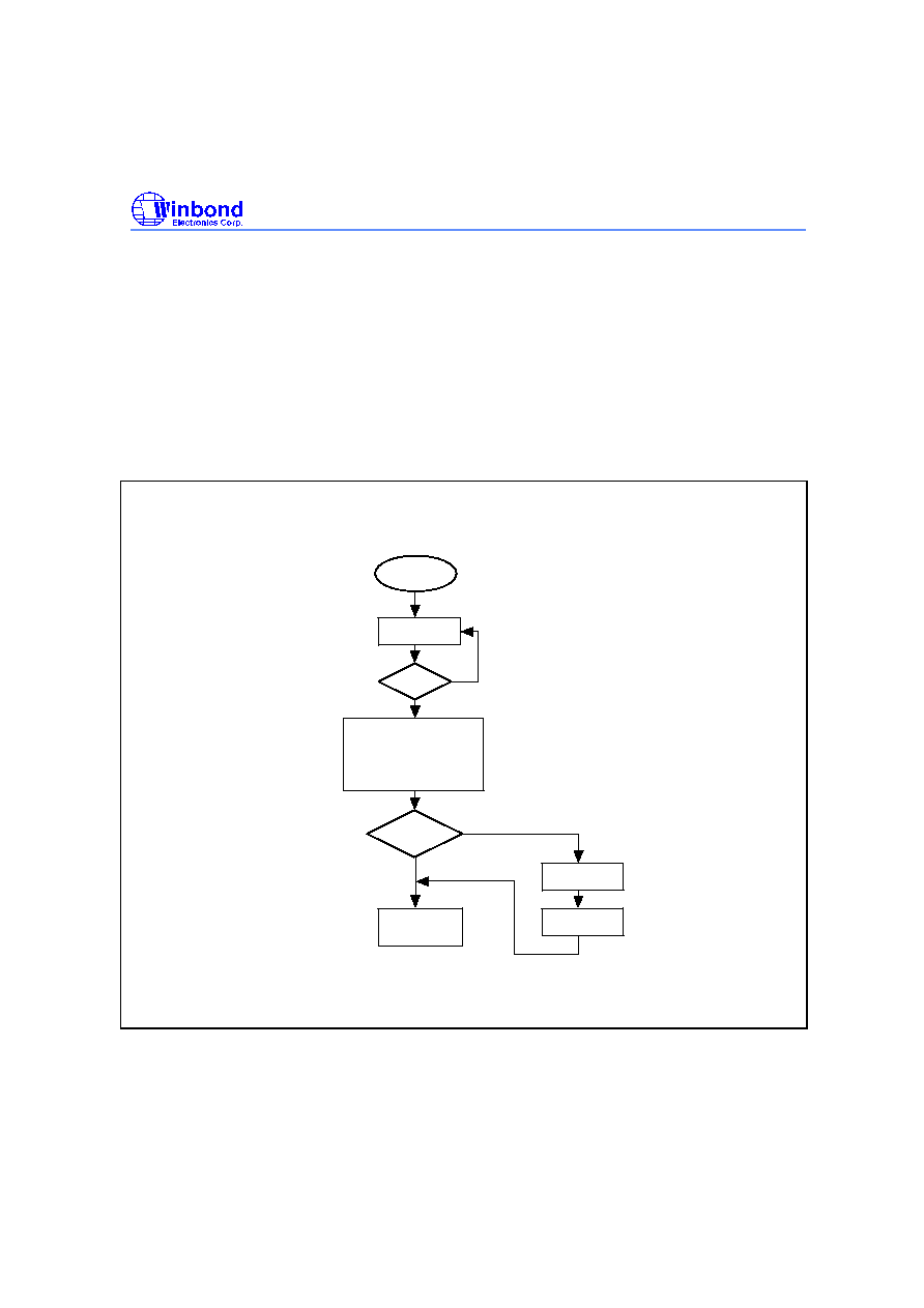
Stop Mode Operation Flow Chart
START
STOP
Enter STOP Mode
INT Enable?
Yes
No
INT Vector
RTNI
PC
PC + 1
STOP
Release
No
Yes
(Only falling signal on
INT0 or P4.0 - P4.2)
(PA, PB Ports on
low level state)
System will Delay 256
Machine Cycle
Automatically
Next
Instruction

W921E880A/W921C880
Publication Release Date: July 1999
- 39 - Revision A3
6.14 Initial Condition Register of EPROM Program Method
There is one 4-bit of the initial condition register (not part of the RAM) in W921E880A to control the
micro-controller initial status after power-on. The format is described as following:
INI register: (initial value = 0FH)
b3
b2
b1
b0
0: osc acts as RC oscillator type
1: osc acts as crystal type
Reserved
Reserved
f
f
0: f1 = f , f2 = f
H
L
1: f1 = f , f2 = f
H
L
6.15 Reset
1. Reset by RESET
256 machine
cycle
Reset all
control reg.
Program executed from
address 000H
RESET
As RESET pin is pulled low, system and all control registers are reset to initial state. After RESET
pin is in high level, system will delay 256 machine cycle time then program is executed from address
000H.
2. Reset by Watch Dog Timer
Reset all control
regs except
STTM0.1.
256 machine
cycle
STTM0.1
Program executed from
address 000H
As watch dog timer underflows, the STTM0.1 is set, in the mean while, system and all control
registers, except data 1 in STTM0.1 bit is reserved, are reset to initial state then after a delay of 256
machine cycle time program is executed from address 000H. After system reset, user can detect
STTM0.1 to recognize which method of reset was done before.
W921E880A/W921C880
- 40 -
7. ADDRESSING MODE
7.1 ROM Addressing Mode
There are two ROM addressing modes in this chip
* Indirect Call Addressing Mode (0H
-
0FFFH)
* Long Call/Jump Addressing Mode (0H
-
1FFFH)
Indirect Call Addressing Mode (1 Word/2 Cycles)
b3 b2 b1 b0
b9 b8 b7 b6 b5 b4 b3 b2 b1 b0
b12 b11 b10 b9 b8 b7 b6 b5 b4 b3 b2 b1 b0
decoder code
b3 b2 b1 b0
i3 i2 i1 i0
B Register
A Register
0
i3 i2 i1 i0 b3 b2 b1 b0 a3 a2 a1 a0
ROM CODE
PC
Instruction: CALLP
Long Call/Jump Addressing Mode (2 Words/2 Cycles)
b9 b8 b7 b6 b5 b4 b3 b2 b1 b0
b9 b8 b7 b6 b5 b4 b3 b2 b1 b0
b12 b11 b10 b9 b8 b7 b6 b5 b4 b3 b2 b1 b0
decoder code
ROM CODE
PC
Instruction: CALL, JMPL, JB0, JB1, JB2, JB3, JC, JNC, JZ, JNZ
7.2 RAM Addressing Mode
There are three RAM addressing modes.
* Direct Addressing Mode
* Indirect Addressing Mode
* Working Register Addressing Mode
W921E880A/W921C880
Publication Release Date: July 1999
- 41 - Revision A3
Direct Addressing Mode (2 Words/2 Cycles)
b9 b8 b7 b6 b5 b4 b3 b2 b1 b0
b9 b8 b7 b6 b5 b4 b3 b2 b1 b0
b9 b8 b7 b6 b5 b4 b3 b2 b1 b0
decoder code
ROM CODE
RAM ADDRESS
Instruction: MOV A, Mx; MOV B, Mx; MOV Mx, A; MOV Mx, B; ..., etc.
Indirect Addressing Mode (1 Word/1 Cycle)
b1 b0
b9 b8 b7 b6 b5 b4 b3 b2 b1 b0
b3 b2 b1 b0
b3 b2 b1 b0
U
Register
V
Register
W
Register
RAM ADDRESS
Instruction: MOV A, @M; MOV B, @M; MOV @M, A; ..., etc.
Working REG Addressing Mode (1 Word/1 Cycle)
b9 b8 b7 b6 b5 b4 b3 b2 b1 b0
decoder code
0 0 0 1 0 0 m3 m2 m1 m0
ROM CODE
RAM ADDRESS
Instruction: MOV A, WRn; MOV WRn, A; ..., etc.
W921E880A/W921C880
- 42 -
7.3 Look-up Table Addressing Mode (1 Word/2 Cycles)
There is one special function look-up table addressing mode in this chip; the instruction is TBL I and
the function is shown in the following table.
b3 b2 b1 b0
b9 b8 b7 b6 b5 b4 b3 b2 b1 b0
b7 b6 b5 b4 b3 b2 b1 b0
decoder code
b3 b2 b1 b0
b11 b10 b9 b8
b12
0
ROM ADDRESS
(0 to 4K)
b9 b8 b7 b6 b5 b4 b3 b2 b1 b0
b3 b2 b1 b0
b3 b2 b1 b0
OP2
OP1
X Y
X
Y
0
0
0
1
1
0
1
1
OP2
OP1
Disable
Disable
B register
A register
Port P2
Both
I3 to I0
B register
A register
ROM CODE
ROM CODE
ROM Code Output to Register or Port
Both
Port P1
Example:
.
.
.
MOV A, #03H
MOV B, #01H
TBL 02H ; A = 0CH, B = Port2 = 0DH
.
.
.
ORG 213H
DC 3DCH
.
.
.

W921E880A/W921C880
Publication Release Date: July 1999
- 43 - Revision A3
8. SPECIAL CONTROL REG. FORMAT
ADDR.
DESCRIPTION
ABBREVIATION
INITIAL VALUE
000H
System Clock Control Register
(SYSCCR)
00H
001H
Bank Select Register
(BKSR)
02H
002H
Reserved
-
-
003H
Port P4 Pull High Resistor Register
(P4PH)
00H
004H
Port P4 Output Type Register
(P4TP)
00H
005H
Port P6 Pull High Resistor Register
(P6PH)
00H
006H
Port P6 Output Type Register
(P6TP)
00H
007H
Port PABCD Pull High Resistor Register
(PABCDPH)
00H
008H
Port PABCD Output Type Register
(PABCDTP)
00H
009H
Serial LSB Nibble Register
(SRLNR)
02H
00AH
Serial MSB Nibble Register
(SRMNR)
00H
00BH
Serial Speed Control Register
(SRSPC)
00H
00CH
Serial Clock Inverter Control Register
(SRINV)
00H
00DH
Port P2 Output Type Register
(P2TP)
00H
00EH
Reserved
-
00FH
Port P3 I/O Status Control Register
( P3IO )
00H
010H
Port P4 I/O Status Control Register
( P4IO )
00H
011H
Port P5 I/O Status Control Register
( P5IO )
00H
012H
Port P6 I/O Status Control Register
( P6IO )
00H
013H
DTMF Oscillation Control Register
(OSCCTR)
00H
014H
DTMF Register
(DTMF)
00H
015H
Row/Column Frequency Control Register
(RCCTL)
00H
016H
D/A Control Register
(DACTL)
00H
017H
D/A Converter LSB Data Register
(DALSB)
00H
018H
D/A Converter MSB Data Register
(DAMSB)
00H
019H
Comparator Analog Input Multiplexer
(ANIMUX)
00H
01AH
Comparator Control Register
(COMPTR)
04H
01BH
Reserved
-
01CH
TM1 Read Only MSB Data Register
(TM1RM)
0FH
01DH
TM1 Read Only LSB Data Register
(TM1RL)
0FH
01EH
TM2 Read Only MSB Data Register
(TM2RM)
0FH
01FH
TM2 Read Only LSB Data Register
(TM2LM)
0FH
020H
TM0 Control Register
(TM0CR)
00H
021H
TM0 MSB Data Register
(TM0MSB)
0FH

W921E880A/W921C880
- 44 -
8. Special Control REG. Format, continued
ADDR.
DESCRIPTION
ABBREVIATION
INITIAL VALUE
022H
TM0 LSB Data Register
(TM0LSB)
0FH
023H
TM0 Status Register
(STTM0)
00H
024H
Reserved or Timer 0 Low Speed Register
(TM0LSR)
00H
025H
TM1 Control Register
(TM1CR)
00H
026H
TM1 MSB Data Register
(TM1MSB)
0FH
027H
TM1 LSB Data Register
(TM1LSB)
0FH
028H
TM1 Status Register
(STTM1)
00H
029H
TM1 Trigger Condition Register
(TGTM1)
00H
02AH
TM2 Control Register
(TM2CR)
00H
02BH
TM2 MSB Data Register
(TM2MSB)
0FH
02CH
TM2 LSB Data Register
(TM2LSB)
0FH
02DH
TM2 Status Register
(STTM2)
00H
02EH
TM2 Trigger Condition Register
(TGTM2)
00H
02FH
TM3 Control Register
(TM3CR)
00H
030H
TM3 MSB Data Register
(TM3MSB)
0FH
031H
TM3 LSB Data Register
(TM3LSB)
0FH
032H
TM3 Status Register
(STTM3)
00H
033H
Reserved
-
034H
Interrupt Enable Flag
(ENINT)
00H
035H
Stop Mode Released Flag
(STPRF)
08H
036H
Hold Mode Released Flag 1
(HMRF1)
00H
037H
Hold Mode Released Flag 2
(HMRF2)
00H
038H
Hold Mode Released Flag 3
(HMRF3)
00H
039H
Interrupt Control Register 1
(INTCT1)
00H
03AH
Interrupt Control Register 2
(INTCT2)
00H
03BH
Interrupt Control Register 3
(INTCT3)
00H
03CH
Hold Released Status Flag 1
(HRSTS1)
00H
03DH
Hold Released Status Flag 2
(HRSTS2)
00H
03EH
Hold Released Status Flag 3
(HRSTS3)
00H
03FH
Beep Tone Generator Register
(BTGR)
00H
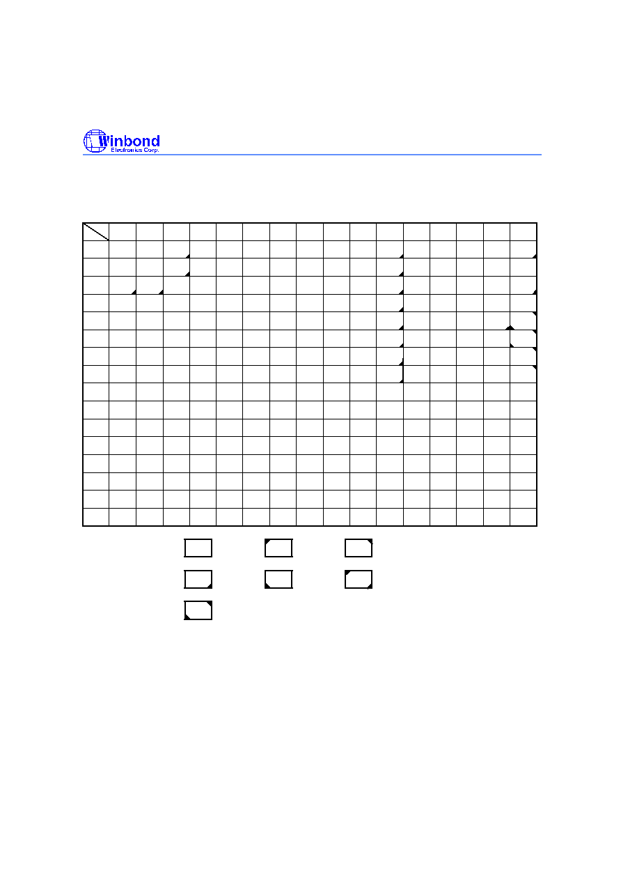
W921E880A/W921C880
Publication Release Date: July 1999
- 45 - Revision A3
9. INSTRUCTION MAP
b9 = 0
b8 = 0
0
1
2
3
4
5
6
0
1
2
3
4
5
6
7
8
9
0A
0B
0C
0D
0E
0F
LSB
MSB
7
8
9
0A 0B 0C 0D 0E 0F
1W/1C
1W/2C
1W/3C
2W/2C
2W/3C
3W/3C
Undecided
ADD A, #I
ADC A, #I
SUB A, #I
SBC A, #I
ANL A, #I
ORL A, #I
XRL A, #I
CMP A, #I
NOP
MOV B, A
MOV Mx, A
MOV @M, A
MOV W, A
MOV V, A
MOV U, A
MOV A, B
MOV Mx, B
MOV @M, B
MOV A, Mx
MOV B, Mx
MOV A, @M
MOV A,W
MOV A, V
MOV A, U
ADD A, Mx
ADC A, Mx
SUB A, Mx
SBC A, Mx
ADD A, @M
ADC A, @M
SUB A, @M
SBC A, @M
ANL A, Mx
ORL A, Mx
XRL A,Mx
CMP A,MX
ANL A, @M
ORL A, @M
XRL A,@M
CMP A,@M
INC B
DEC B
INC DP
DEC DP
CLRB Mx, bit
CLRB @M, bit
SETB Mx, bit
SETB @M, bit
CLR EVF
SET CF
MOV B, @M
SRL A
XCH A, B
SOP
SIP
RTN
RTNI
HOLD
STOP
SRH A
SLL A
SLH A
RRC A
RLC A
XCH V.CV
XCH U,CU
MOV DP, #I
XRL A,B
CMP A,B
CLR CF

W921E880A/W921C880
- 46 -
b9 = 1
b8 = 0
0
1
2
3
4
5
6
0
1
2
3
4
5
6
7
8
9
0A
0B
0C
0D
0E
0F
LSB
MSB
7
8
9
0A 0B 0C 0D 0E 0F
1W/1C
1W/2C
1W/3C
2W/2C
2W/3C
3W/3C
Undecided
JB0
JB2
JC
JZ
JMPL
JB1
JB3
JNC
JNZ
CALL
CALLP
TBL
MOV PMx, #I

W921E880A/W921C880
Publication Release Date: July 1999
- 47 - Revision A3
b9 = 1
b8 = 1
0
1
2
3
4
5
6
0
1
2
3
4
5
6
7
8
9
0A
0B
0C
0D
0E
0F
LSB
MSB
7
8
9
0A 0B 0C 0D 0E 0F
1W/1C
1W/2C
1W/3C
2W/2C
2W/3C
3W/3C
Undecided
MOV A, #I
MOV B, #I
MOV Mx, #I
MOV @M, #I
MOV A, WRn
MOV B, WRn
MOV WRn, A
MOV WRn, B
MOV A, Px
MOV B, Px
MOV Px, A
MOV Px, B
ADD A, WRn
ADC A, WRn
SUB A, WRn
SBC A, WRn
ANL A, WRn
ORL A, WRn
XRL A, WRn
CMP A, WRn

W921E880A/W921C880
- 48 -
10. INSTRUCTION SETS
MACHINE CODE
MNEMONIC
FUNCTION
A B U V W STATUS W/C
MEMO
Arithmetic
00 0000 1010, xxxxxxxxxx
ADD A, Mx
A + Mx
A
A
Z, C
2/2
11 0100 0 i i i
ADD A, WRx
A + WRx
A
A
Z, C
1/1
x = 0 -- 7
00 0000 1011
ADD A, @M
A + @M
A
A U V W
Z, C
1/1
00 0001 1010, xxxxxxxxxx
ADC A, Mx
A + Mx + C
A
A
Z, C
2/2
11 0100 1 i i i
ADC A, WRx
A + WRx + C
A
A
Z, C
1/1
x = 0 -- 7
00 0001 1011
ADC A,@M
A+ @M + C
A
A U V W
Z, C
1/1
00 0010 1010, xxxxxxxxxx
SUB A, Mx
A - Mx
A
A
Z, C
2/2
11 0101 0 i i i
SUB A, WRx
A - WRx
A
A
Z, C
1/1
x = 0 -- 7
00 0010 1011
SUB A, @M
A - @M
A
A U V W
Z, C
1/1
00 0011 1010, xxxxxxxxxx
SBC A, Mx
A - Mx - C
A
A
Z, C
2/2
11 0101 1 i i i
SBC A, WRx
A - WRx - C
A
A
Z, C
1/1
x = 0 -- 7
00 0011 1011
SBC A, @M
A - @M - C
A
A U V W
Z, C
1/1
00 1000 i i i i
ADD A, #I
A + I
A
A
Z, C
1/1
00 1001 i i i i
ADC A, #I
A + I +C
A
A
Z. C
1/1
00 1010 i i i i
SUB A, #I
A - I
A
A
Z, C
1/1
00 1011 i i i i
SBC A, #I
A - I - C
A
A
Z, C
1/1
00 1010 0001
DEC A
A - 1
A
A
Z, C
1/1
SUB A, #1
00 0010 1001
DEC B
B - 1
B
B
Z, C
1/1
00 0011 1001
DEC DP
DP - 1
DP
U V W
C
1/1
00 1000 0001
INC A
A + 1
A
A
Z, C
1/1
ADD A, #1
00 0000 1001
INC B
B + 1
B
B
Z, C
1/1
00 0001 1001
INC DP
DP + 1
DP
U V W
C
1/1
Logic
00 0100 1010, xxxxxxxxxx
ANL A, Mx
A ^ Mx
A
A
Z
2/2
11 0110 0 i i i
ANL A, WRx
A ^ WRx
A
A
Z
1/1
x = 0 -- 7
00 0100 1011
ANL A, @M
A ^ @M
A
A U V W
Z
1/1
00 0101 1010, xxxxxxxxxx
ORL A, Mx
A
Mx
A
A
Z
2/2
11 0110 1 i i i
ORL A, WRx
A
WRx
A
A
Z
1/1
x = 0 -- 7
00 0101 1011
ORL A, @M
A
@M
A
A U V W
Z
1/1
00 0110 1010, xxxxxxxxxx
XRL A, Mx
A
Mx
A
A
Z
2/2
11 0111 0 i i i
XRL A, WRx
A
WRx
A
A
Z
1/1
x = 0 -- 7
00 0110 1011
XRL A, @M
A
@M
A
A U V W
Z
1/1
00 0111 1010, xxxxxxxxxx
CMP A, Mx
A - Mx
Z, C
2/2
11 0111 1 i i i
CMP A, WRx
A - WRx
Z, C
1/1
x = 0 -- 7

W921E880A/W921C880
Publication Release Date: July 1999
- 49 - Revision A3
10. Instruction set, continued
MACHINE CODE
MNEMONIC
FUNCTION
A B U V W STATUS W/C
MEMO
00 0111 1011
CMP A, @M
A - @M
U V W
Z, C
1/1
00 0110 1001
XRL A, B
A
B
A
A B
Z
1/1
00 0111 1001
CMP A, B
A - B
Z, C
1/1
00 1100 i i i i
ANL A, #I
A ^ I
A
A
Z
1/1
00 1101 i i i i
ORL A, #I
A
I
A
A
Z
1/1
00 1110 i i i i
XRL A, #I
A
I
A
A
Z
1/1
00 1111 i i i i
CMP A, #I
A - I
Z, C
1/1
00 1110 1111
NOT A
NOT A
A
A
Z
1/1
XRL A,#F
Move
00 0000 0001
MOV A, B
B
A
A B
Z
1/1
00 0000 0010, xxxxxxxxxx
MOV A, Mx
Mx
A
A
Z
2/2
00 0000 0011
MOV A, @M
@M
A
A U V W
Z
1/1
00 0000 0100
MOV A, W
W
A
A
W
Z
1/1
00 0000 0101
MOV A, V
V
A
A
V
Z
1/1
00 0000 0110
MOV A, U
U
A
A U
Z
1/1
00 0001 0000
MOV B, A
A
B
A B
--
1/1
00 0010 0000, xxxxxxxxxx
MOV Mx, A
A
Mx
A
--
2/2
00 0011 0000
MOV @M, A
A
@M
A U V W
--
1/1
00 0100 0000
MOV W, A
A
W
A
W
--
1/1
00 0101 0000
MOV V, A
A
V
A
V
--
1/1
00 0110 0000
MOV U, A
A
U
A U
--
1/1
00 0001 0010, xxxxxxxxxx
MOV B, Mx
Mx
B
B
--
2/2
00 0001 0011
MOV B, @M
@M
B
B U V W
--
1/1
00 0010 0001, xxxxxxxxxx
MOV Mx, B
B
Mx
B
--
2/2
00 0011 0001
MOV @M,B
B
@M
B U V W
--
1/1
11 0000 i i i i
MOV A, #I
I
A
A
Z
1/1
11 0001 i i i i
MOV B, #I
I
B
B
--
1/1
11 0010 i i i i, xxxxxxxxxx
MOV Mx, #I
I
Mx
--
2/2
11 0011 i i i i
MOV @M, #I
I
@M
U V W
--
1/1
11 1000 nnnn
MOV A, WRn
WRn
A
A
Z
1/1
11 1001 xxxx
MOV A, Px
Px
A
A
Z
1/1
11 1010 nnnn
MOV B, WRn
WRn
B
B
--
1/1
11 1011 xxxx
MOV B, Px
Px
B
B
--
1/1
11 1100 nnnn
MOV WRn, A
A
WRn
A
--
1/1
11 1101 nnnn
MOV Px, A
A
Px
A
--
1/1
11 1110 xxxx
MOV WRn, B
B
WRn
B
--
1/1
W921E880A/W921C880
- 50 -
10. Instruction set, continued
MACHINE CODE
MNEMONIC
FUNCTION
A B U V W STATUS W/C
MEMO
11 1111 xxxx
MOV Px, B
B
Px
B
--
1/1
10 0xxx i i i i
MOV PMx, #I
I
PMx
--
1/1
Mode of Port 0
-
7
SERIAL I/O
00 0100 1111
SOP
--
--
*1
00 0101 1111
SIP
--
--
*1
Rotate or Shift
00 0000 1000
SRL A
An
An-1, 0
A3
A
Z
1/1
n = 3
-
1
00 0001 1000
SRH A
An
An-1, 1
A3
A
Z
1/1
n = 3
-
1
00 0010 1000
SLL A
An
An+1, 0
A0
A
Z
1/1
n = 0
-
2
00 0011 1000
SLH A
An
An+1, 1
A0
A
Z
1/1
n = 0
-
2
00 0100 1000
RRC A
An
An-1,A0
C,C
A3
A
Z, C
1/1
n = 3
-
1
00 0110 1000
RLC A
An
An+1,A3
C,C
A0
A
Z, C
1/1
n = 0
-
2
Branch
10 1000 0aaa, aaaaaaaaaa
JB0 addr
Addr
PC
--
2/2
10 1000 1aaa, aaaaaaaaaa
JB1 addr
Addr
PC
--
2/2
10 1001 0aaa, aaaaaaaaaa
JB2 addr
Addr
PC
--
2/2
10 1001 1aaa, aaaaaaaaaa
JB3 addr
Addr
PC
--
2/2
10 1010 0aaa, aaaaaaaaaa
JC addr
Addr
PC
--
2/2
10 1010 1aaa, aaaaaaaaaa
JNC addr
Addr
PC
--
2/2
10 1011 0aaa, aaaaaaaaaa
JZ addr
Addr
PC
--
2/2
10 1011 1aaa, aaaaaaaaaa
JNZ addr
Addr
PC
--
2/2
10 1100 0aaa, aaaaaaaaaa
JMPL addr
Addr
PC
--
2/2
Long Jump
10 1100 1aaa, aaaaaaaaaa
CALL addr
Addr
PC
--
2/2
10 1101 aaaa
CALLP addr
@Addr
PC
A B
--
1/2
Indirect address
call
10 1110 aaaa
TBL addr
--
A B
Z
1/2
Look Up Table
Other
00 0110 1111
RTN
Stack
PC
--
1/3
00 0111 1111
RTNI
Stack
PC, Z, C
Z,C
1/3
ENINT active again
00 0000 0000
NOP
--
--
1/1
00 0110 1110
HOLD
--
--
1/1
00 0111 1110
STOP
--
--
1/1
00 0001 11bb
CLRB @M, bit
0
@M(b)
U V W
--
1/1

W921E880A/W921C880
Publication Release Date: July 1999
- 51 - Revision A3
10. Instruction set, continued
MACHINE CODE
MNEMONIC
FUNCTION
A B U V W STATUS W/C
MEMO
00 0000 11bb, xxxxxxxxxx
CLRB Mx, bit
0
Mx(b)
--
2/2
00 0011 11bb
SETB @M, bit
1
@M(b)
U V W
--
1/1
00 0010 11bb, xxxxxxxxxx
SETB Mx, bit
1
Mx(b)
--
2/2
00 0111 1100
CLR CF
0
C
C
1/1
11 0000 0000
CLR A
0
A
A
Z
1/1
MOV A, #0
00 0100 1100, 00i i i i i i i i
CLR EVF, #I
--
--
2/2
00 0110 1100
SET CF
C = 1
C
1/1
00 0100 1110, i i i i i i i i i i
MOV DP, #I
I
DP
U V W
--
2/2
00 0111 1101
XCH U, CU
U
CU
U
--
1/1
00 0110 1101
XCH V, CV
V
CV
V
--
1/1
00 0100 1101
XCH A, B
A
B
A B
Z
1/1
Notes:
*DP = {W reg , V reg , U reg}
*@M = @{W, V, U}
*@Addr = { I , Breg, Areg} to be a target address for the CALLP instruction
*1: Depends on the SRMNR, SRLNR register
11. ABSOLUTE MAXIMUM RATINGS
PARAMETER
RATING
UNIT
Supply Voltage to Ground Potential
-0.3 to +7.0
V
Applied input/output Voltage
-0.3 to +7.0
V
Power Dissipation
120
mW
Ambient Operating Temperature
0 to +70
�
C
Storage Temperature
-55 to 150
�
C
Note: Exposure to conditions beyond those listed under Absolute Maximum Ratings may adversely affect the life and reliability of the
device.
W921E880A/W921C880
- 52 -
12. ELECTRICAL CHARACTERISTICS
12.1 AC Characteristics
W921E880A EPROM Type
(V
DD
-
V
SS
= 3.0V, F
OSC
= 4.0 MHz, T
A
= 25
�
C, unless otherwise specified)
PARAMETER
SYM.
CONDITIONS
MIN.
TYP. MAX. UNIT
Operating Frequency 1
F
OSC
1
OSCI, OSCO
--
400
--
KHz
Operating Frequency 2
F
OSC
2
OSCI, OSCO
--
800
--
KHz
Operating Frequency 3
F
OSC
3
OSCI, OSCO
--
2
--
MHz
Operating Frequency 4
F
OSC
4
OSCI, OSCO
--
3.58
--
MHz
Operating Frequency 5
F
OSC
5
OSCI, OSCO
--
4
--
MHz
Operating sub. system
F
SUB
XT, XT
--
32.768
--
KHz
Instruction Cycle Time
T
I
One Machine Cycle
--
4/F
OSC
--
S
Serial Port Data Ready Time
T
DR
--
200
--
--
nS
Serial Port Data Hold Time
T
DH
--
200
--
--
nS
RESET Active Width
T
RAW
--
2T
I
--
--
T
I
ROW 1 Frequency (697Hz)
F
ROW
1 F
OSC
= 4 MHz, 2 MHz
800 KHz, 400 KHz
-0.5
--
+0.5
%
ROW 2 Frequency (770 Hz)
F
ROW
2
''
-0.5
--
+0.5
%
ROW 3 Frequency (852 Hz)
F
ROW
3
''
-0.5
--
+0.5
%
ROW 4 Frequency (941 Hz)
F
ROW
4
''
-0.5
--
+0.5
%
COL 1 Frequency (1209 Hz)
F
COL
1
''
-0.5
--
+0.5
%
COL 2 Frequency (1336 Hz)
F
COL
2
''
-0.5
--
+0.5
%
COL 3 Frequency (1477 Hz)
F
COL
3
''
-0.5
--
+0.5
%
COL 4 Frequency (1633 Hz)
F
COL
4
''
-0.5
--
+0.5
%
ROW 1 Frequency (697 Hz)
F
ROW
1
F
OSC
= 3.58 MHz
-0.92
--
+0.92
%
ROW 2 Frequency (770 Hz)
F
ROW
2
''
-0.92
--
+0.92
%
ROW 3 Frequency (852 Hz)
F
ROW
3
''
-0.92
--
+0.92
%
ROW 4 Frequency (941 Hz)
F
ROW
4
''
-0.92
--
+0.92
%
COL 1 Frequency (1209 Hz)
F
COL
1
''
-0.92
--
+0.92
%
COL 2 Frequency (1336 Hz)
F
COL
2
''
-0.92
--
+0.92
%
COL 3 Frequency (1477 Hz)
F
COL
3
''
-0.92
--
+0.92
%
COL 4 Frequency (1633 Hz)
F
COL
4
''
-0.92
--
+0.92
%
Oscillator Start Time
T
OST
OSCO, XT
--
2
17
/
F
OSC
--
mS
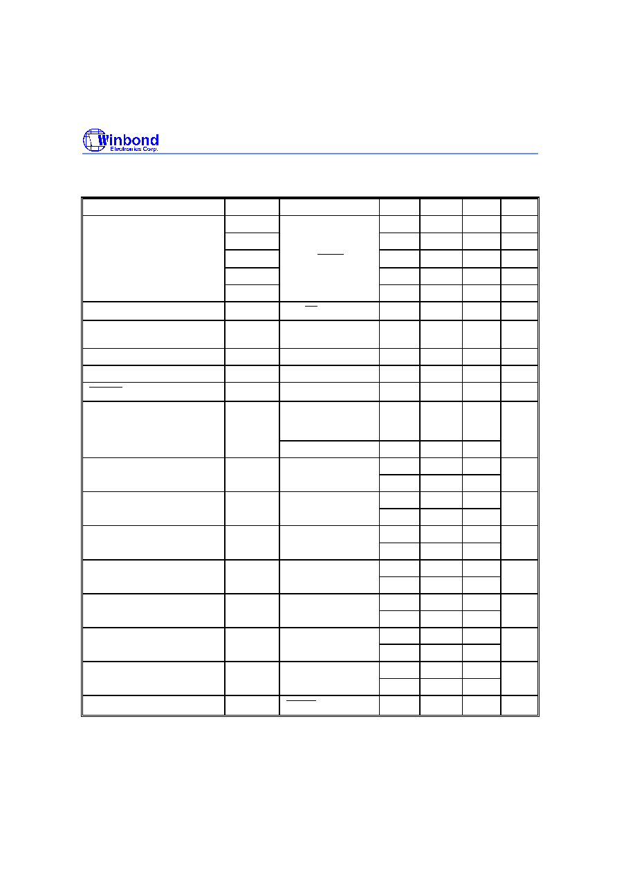
W921E880A/W921C880
Publication Release Date: July 1999
- 53 - Revision A3
W921C880 Mask ROM Type
(V
DD
-
V
SS
= 3.0V, F
OSC
= 4.0 MHz, T
A
= 25
�
C, unless otherwise specified)
PARAMETER
SYM.
CONDITIONS
MIN.
TYP. MAX. UNIT
F
OSC1
-
400
-
KHz
F
OSC2
-
800
-
KHz
Operating Frequency
F
OSC3
OSCI,
OSCO
-
2
-
MHz
F
OSC4
-
3.58
-
MHz
F
OSC5
-
4
-
MHz
Operating Sub-frequency
F
SUB
XT,
XT
-
32.768
-
KHz
Instruction Cycle Time
T
I
One Machine
Cycle
-
4/F
OSC
-
S
Serial Port Data Ready Time
T
DR
-
200
-
-
nS
Serial Port Data Hold Time
T
DH
-
200
-
-
nS
RESET Active Width
T
RAW
-
2
-
-
T
I
ROW 1 Frequency (697Hz)
F
ROW1
F
OSC
= 4 MHz,
2 MHz, 800 KHz,
400 KHz
-0.5
-
+0.5
%
F
OSC
= 3.58 MHz
-0.92
-
+0.92
ROW 2 Frequency (770 Hz)
F
ROW2
Same as ROW1
-0.5
-
+0.5
%
-0.92
-
+0.92
ROW 3 Frequency (852 Hz)
F
ROW3
Same as ROW1
-0.5
-
+0.5
%
-0.92
-
+0.92
ROW 4 Frequency (941 Hz)
F
ROW4
Same as ROW1
-0.5
-
+0.5
%
-0.92
-
+0.92
COL 1 Frequency (1209 Hz)
F
COL1
Same as ROW1
-0.5
-
+0.5
%
-0.92
-
+0.92
COL 2 Frequency (1336 Hz)
F
COL2
Same as ROW1
-0.5
-
+0.5
%
-0.92
-
+0.92
COL 3 Frequency (1477 Hz)
F
COL3
Same as ROW1
-0.5
-
+0.5
%
-0.92
-
+0.92
COL 4 Frequency (1633 Hz)
F
COL4
Same as ROW1
-0.5
-
+0.5
%
-0.92
-
+0.92
Oscillator Start Time
T
OST
OSCO
-
2
17
/F
OSC
-
mS

W921E880A/W921C880
- 54 -
12.2 DC Characteristics
W921E880A EPROM Type
(V
DD
-
V
SS
= 3.0V, F
OSC
= 4.0 MHz, T
A
= 25
�
C, unless otherwise specified)
PARAMETER
SYM.
CONDITIONS
MIN.
TYP.
MAX. UNIT
Operating Voltage
V
DD
--
2.8
3.0
5.5
V
Operating Current 1 (4 MHz)
(Active mode)
I
OP
1
Analog active.
V
DD
= 5V
--
9
12
mA
Operating Current 2 (4 MHz)
(Active mode)
I
OP
2
Analog disable
V
DD
= 5V
--
5
8
mA
Operating Current 3 (800 KHz)
(Active mode)
I
OP
3
Analog active.
V
DD
= 3V
--
3.1
4.3
mA
Operating Current 4 (800 KHz)
(Active mode)
I
OP
4
Analog disable
V
DD
= 3V
--
0.6
1.8
mA
Operating Current 5 (400 KHz)
(Active mode)
I
OP
5
Analog active.
V
DD
= 3V
--
1.0
2.0
mA
Operating Current 6 (400 KHz)
(Active mode)
I
OP
6
Analog disable
V
DD
= 3V
--
0.4
1.0
mA
Hold Mode Current 1 (4 MHz)
I
HM
1
V
DD
= 5V
--
1.2
2.0
mA
Hold Mode Current 2 (800 KHz)
I
HM
2
V
DD
= 3V
--
0.2
0.7
mA
Hold Mode Current 3 (400 KHz)
I
HM
3
V
DD
= 3V
--
0.1
0.4
mA
Hold Mode Current 4 (32.768
KHz)
I
HM
4
V
DD
= 3V
--
50
80
�
A
Stop Mode Current 1 (4 MHz)
I
SM
1
V
DD
= 5V
--
2.0
3.0
�
A
Stop Mode Current 2 (800 KHz)
I
SM
2
V
DD
= 3V
--
1.0
3.0
�
A
Stop Mode Current 3 (400 KHz)
I
SM
3
V
DD
= 3V
--
1.0
3.0
�
A
Stop Mode Current 4 (32.768
KHz)
I
SM
4
V
DD
= 3V
--
1.0
3.0
�
A
Input High Voltage
V
IH
--
0.7 V
DD
--
V
DD
V
DD
Input Low Voltage
V
IL
--
0
--
0.3 V
DD
V
DD
Pull-high Resistor
(P2, P4, P6, P7, P9, PA, PB,
PC, PD)
R
PH
V
DD
= 3V
--
400
--
K
Output High Voltage
(P0, P1, P8)
V
OH
1 V
DD
= 4.5 to 5.5V
I
OH
= -10 mA
2.0
--
--
V
(The other ports)
V
OH
2
I
OH
= -0.5 mA
V
DD
-1.0
--
--
V
Output Low Voltage
(P2, P7, P9)
V
OL
1
V
DD
= 4.5 to 5.5V
I
OL
= 15 mA
--
--
2.0
V
(The other ports)
V
OL
2
I
OL
= 0.4 mA
--
--
0.4
V
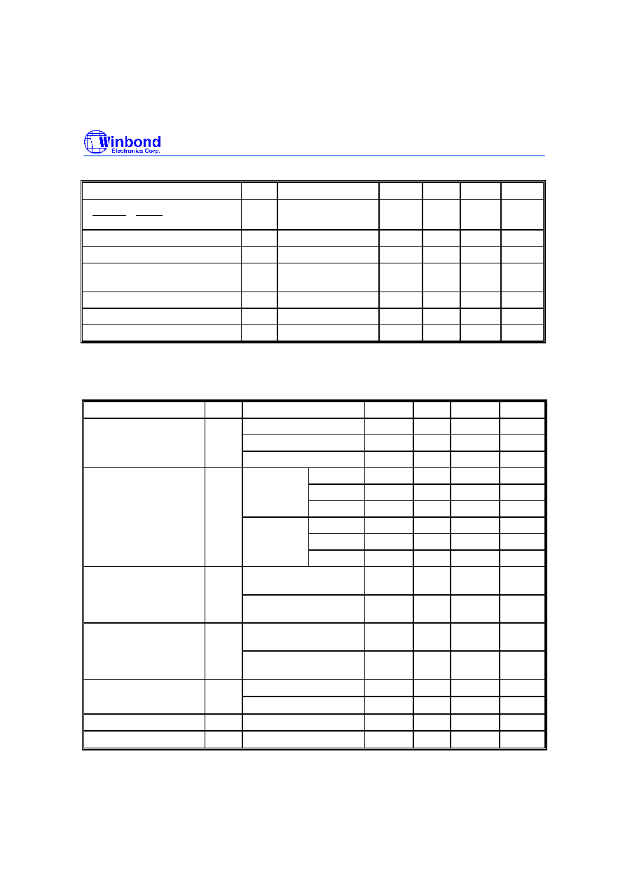
W921E880A/W921C880
Publication Release Date: July 1999
- 55 - Revision A3
W921E880A EPROM TYPE DC Characteristics, continued
PARAMETER
SYM.
CONDITIONS
MIN.
TYP. MAX. UNIT
Input Leakage Current
(RESET , TEST )
V
IL
V
IN
= 0V
--
--
1
�
A
DTMF Output DC Level
V
TDC
V
DD
= 2.8 to 5.5V
1.0
--
3.0
V
DTMF Distortion
V
DD
-
-30
-23
dB
DTMF Output Voltage
V
TO
ROW Group,
R
L
= 5 K
130
150
170
mVrm
s
Pre-emphasis
COL/ROW
1
2
3
dB
D/A DC Voltage Reference
V
REF
--
0
--
2/3
V
DD
D/A Resoultion
V
RSL
--
--
1/256
--
V
DAC
W921C880 Mask ROM Type
(V
DD
-
V
SS
= 3.0V, F
OSC
= 4.0 MHz, T
A
= 25
�
C, unless otherwise specified)
PARAMETER
SYM.
CONDITIONS
MIN.
TYP.
MAX.
UNIT
Operating Voltage
V
DD
4 MHz
2.4
-
5.5
V
2 MHz
2.0
-
5.5
V
400 KHz
2.0
-
5.5
V
Operating Current
I
OP
4 MHz
--
1.0
--
mA
(Active Mode)
V
DD
= 3V
2 MHz
--
0.7
--
mA
(Analog all off)
400 KHz
--
0.4
--
mA
4 MHz
--
2.5
--
mA
V
DD
= 5V
2 MHz
--
2.2
--
mA
400 KHz
--
1.5
--
mA
Hold Mode Current
I
HM1
V
DD
= 3V, F
OSC
= 4
MHz
--
0.5
--
mA
(Analog all off)
V
DD
= 5V, F
OSC
= 4
MHz
--
2.0
--
mA
Hold Mode Current
I
HM2
V
DD
= 3V,
F
OSC
= 32.768 KHz
--
10
--
�
A
(Analog all off)
V
DD
= 5V,
F
OSC
= 32.768 KHz
--
50
--
�
A
Stop Mode Current
I
SM
V
DD
= 3V
-
1.0
3.0
�
A
V
DD
= 5V
-
1.0
3.0
�
A
Input High Voltage
V
IH
-
0.7 V
DD
-
V
DD
V
DD
Input Low Voltage
V
IL
-
0
-
0.3 V
DD
V
DD

W921E880A/W921C880
- 56 -
W921C880 Mask ROM Type, continued
PARAMETER
SYM.
CONDITIONS
MIN.
TYP.
MAX.
UNIT
Pull-high Resistor
(P2, P4, P6, PA, PB, PC, PD)
R
PH
V
DD
= 3V
-
400
-
K
Output High Voltage
V
OH
I
OH
= -0.5 mA
V
DD
-
1.0
-
V
Output Low Voltage
V
OL1
I
OL
= 15 mA, port P2
-
-
2.0
V
OL2
I
OL
= 0.4 mA, Other ports
-
-
0.4
V
Input Leakage Current
V
IL
V
IN
= 0V, RESET pin
-
-
1
�
A
DTMF Output DC Level V
TDC
V
DD
= 2.8 to 5.5V
1.0
-
3.0
V
DTMF Distortion
THD V
DD
= 2.8 to 5.5V
-
-30
-23
dB
DTMF Output Voltage
V
TO
ROW Group, RL = 5 K
130
150
170
mVrms
Pre-emphasis
Col/Row
V
DD
= 3.0 to 5.5V
1
2
3
dB
D/A DC Reference
Voltage
V
REF
-
0
-
2/3
V
DD
D/A Resolution Voltage
V
RSL
-
-
1/256
-
V
DAC
13. PACKAGE DIMENSIONS
80-pin QFP
41
40
25
24
65
1
80
2
1
A
H
D
D
e
b
E
H
E
y
A
A
Seating Plane
L
L
1
See Detail F
Detail F
c
64
1. Dimension D & E do not include interlead
flash.
2. Dimension b does not include dambar
protrusion/intrusion.
3. Controlling dimension: Millimeter
4. General appearance spec. should be based
on final visual inspection spec.
0.10
0
12
0
0.004
2.40
1.40
19.10
1.20
18.80
1.00
18.49
0.094
0.055
0.988
0.752
0.047
0.976
0.740
0.039
0.964
0.728
0.80
20.13
14.13
0.25
0.45
2.97
3.30
20.00
14.00
2.85
19.87
13.87
0.10
0.30
2.73
0.10
0.792
0.556
0.010
0.018
0.117
0.130
0.787
0.551
0.112
0.031
0.782
0.546
0.004
0.012
0.107
0.004
Notes:
Symbol
Min. Nom. Max.
Max.
Nom.
Min.
Dimension in inches
Dimension in mm
A
b
c
D
e
H
D
H
E
L
y
A
A
L
1
1
2
E
0.014
0.006
0.15
0.35
24.49
24.80 25.10
12
0.025
0.037
0.087
0.103
0.65
0.95
2.21
2.62

W921E880A/W921C880
Publication Release Date: July 1999
- 57 - Revision A3
Headquarters
No. 4, Creation Rd. III,
Science-Based Industrial Park,
Hsinchu, Taiwan
TEL: 886-3-5770066
FAX: 886-3-5792766
http://www.winbond.com.tw/
Voice & Fax-on-demand: 886-2-27197006
Taipei Office
11F, No. 115, Sec. 3, Min-Sheng East Rd.,
Taipei, Taiwan
TEL: 886-2-27190505
FAX: 886-2-27197502
Winbond Electronics (H.K.) Ltd.
Rm. 803, World Trade Square, Tower II,
123 Hoi Bun Rd., Kwun Tong,
Kowloon, Hong Kong
TEL: 852-27513100
FAX: 852-27552064
Winbond Electronics North America Corp.
Winbond Memory Lab.
Winbond Microelectronics Corp.
Winbond Systems Lab.
2727 N. First Street, San Jose,
CA 95134, U.S.A.
TEL: 408-9436666
FAX: 408-5441798
Note: All data and specifications are subject to change without notice.