
W925E/C240
8-bit CID Microcontroller
-1-
Release Date : 2002/7/2
Revision : A6
1
GENERAL DESCRIPTION...................................................................................................................... 3
2
FEATURES .................................................................................................................................................. 3
3
PIN CONFIGURATION............................................................................................................................ 5
4
PIN DESCRIPTION ................................................................................................................................... 6
5
BLOCK DIAGRAM ................................................................................................................................... 8
6
FUNCTIONAL DESCRIPTION .............................................................................................................. 9
6.1
M
EMORY
O
RGANIZATION
................................................................................................................... 10
6.2
S
PECIAL
F
UNCTION
R
EGISTERS
........................................................................................................... 13
6.3
I
NITIAL
S
TATE OF
R
EGISTERS
.............................................................................................................. 30
6.4
I
NSTRUCTION
....................................................................................................................................... 31
6.5
P
OWER
M
ANAGEMENT
........................................................................................................................34
6.6
R
ESET
................................................................................................................................................... 35
6.7
I
NTERRUPT
........................................................................................................................................... 35
6.8
P
ROGRAMMABLE
T
IMERS
/C
OUNTERS
................................................................................................ 37
6.9
S
ERIAL
P
ORT
1 .....................................................................................................................................41
6.10
C
OMPARATOR
...................................................................................................................................... 42
6.11
DTMF G
ENERATOR
............................................................................................................................. 43
6.12
FSK G
ENERATOR
................................................................................................................................ 44
6.13
I/O P
ORTS
.............................................................................................................................................45
6.14
D
IVIDER
................................................................................................................................................46
6.15
C
ALLING
I
DENTITY
D
ELIVERY
(CID) ................................................................................................. 47
7
ELECTRICAL CHARACTERISTICS .................................................................................................60
7.1
M
AXIMUM
R
ATINGS
* .......................................................................................................................... 60
7.2
R
ECOMMENDED
O
PERATING
C
ONDITIONS
......................................................................................... 60
7.3
DC E
LECTRICAL
C
HARACTERISTICS
.................................................................................................. 60
7.4
E
LECTRICAL
C
HARACTERISTICS
- G
AIN
C
ONTROL
OP-A
MPLIFIER
.................................................. 62
7.5
AC E
LECTRICAL
C
HARACTERISTICS
.................................................................................................. 62
8
PACKAGE..................................................................................................................................................65
9
VERSION STATEMENT ........................................................................................................................66

W925E/C240
8-bit CID Microcontroller
-2-
Release Date : 2002/7/2
Revision : A6
F
IGURE
3-1 W925E/C240 P
IN
C
ONFIGURATION
.................................................................................................. 5
F
IGURE
6-1 P
ROGRAM
M
EMORY
M
AP
................................................................................................................10
F
IGURE
6-2
MEMORY MAP
.................................................................................................................................... 11
F
IGURE
6-3 S
CRATCHPAD
RAM/R
EGISTER
A
DDRESSING
.................................................................................. 12
F
IGURE
6-4 T
HE
S
TRUCTURE OF
CID F
LAGS
...................................................................................................... 36
F
IGURE
6-5 M
ODE
0 & M
ODE
1
OF
T
IMER
/C
OUNTER
0 & 1.............................................................................. 38
F
IGURE
6-6 M
ODE
2
OF
T
IMER
/C
OUNTER
0 & 1 ................................................................................................ 39
F
IGURE
6-7 W
ATCHDOG
T
IMER
...........................................................................................................................40
F
IGURE
6-8 T
IMING OF THE
S
ERIAL
P
ORT
1 I
NPUT
F
UNCTION
........................................................................... 42
F
IGURE
6-9 T
IMING OF THE
S
ERIAL
P
ORT
1 O
UTPUT
F
UNCTION
....................................................................... 42
F
IGURE
6-10 T
HE
C
ONFIGURATION OF
C
OMPARATOR
....................................................................................... 43
F
IGURE
6-11 T
HE
R
ELATION
B
ETWEEN
DTMF
AND
K
EYPAD
........................................................................... 43
F
IGURE
6-12 FSK M
ODULATOR
.......................................................................................................................... 44
F
IGURE
6-13 13/14-
BIT
D
IVIDER
......................................................................................................................... 46
F
IGURE
6-14 T
HE
CID B
LOCK
D
IAGRAM
........................................................................................................... 47
F
IGURE
6-15 A
PPLICATION
C
IRCUIT OF THE
R
ING
D
ETECTOR
........................................................................... 48
F
IGURE
6-16 D
IFFERENTIAL
I
NPUT
G
AIN
C
ONTROL
C
IRCUIT
............................................................................49
F
IGURE
6-17 S
INGLE
-E
NDED
I
NPUT
G
AIN
C
ONTROL
C
IRCUIT
........................................................................... 49
F
IGURE
6-18 G
UARD
T
IME
W
AVEFORM OF
A
LERT
T
ONE
S
IGNAL
D
ETECTION
................................................50
F
IGURE
6-19 T
HE
W
AVEFORM OF
DTMF D
ETECTION
....................................................................................... 51
F
IGURE
6-20 FSK D
ETECTION
E
NABLE AND
FSK
C
ARRIER
P
RESENT AND
A
BSENT
T
IMING
.......................... 51
F
IGURE
6-21 S
ERIAL
D
ATA
I
NTERFACE
T
IMING OF
FSK D
EMODULATION
....................................................... 52
F
IGURE
6-22 I
NTERNAL
CID G
AIN
C
ONTROL
R
EGISTER
S
ETTING
W
AVEFORM
............................................... 53
F
IGURE
6-23 A
PPLICATION
C
IRCUIT OF
CID ...................................................................................................... 54
F
IGURE
6-24 I
NPUT AND
O
UTPUT
T
IMING OF
B
ELLCORE
O
N
-
HOOK
D
ATA
T
RANSMISSION
............................. 55
F
IGURE
6-25 I
NPUT AND
O
UTPUT
T
IMING OF
B
ELLCORE
O
FF
-
HOOK
D
ATA
T
RANSMISSION
............................56
F
IGURE
6-26 I
NPUT AND
O
UTPUT
T
IMING OF
BT I
DLE
S
TATE
(O
N
-
HOOK
) D
ATA
T
RANSMISSION
.................. 57
F
IGURE
6-27 I
NPUT AND
O
UTPUT
T
IMING OF
BT L
OOP
S
TATE
(O
FF
-
HOOK
) D
ATA
T
RANSMISSION
............... 58
F
IGURE
6-28 I
NPUT AND
O
UTPUT
T
IMING OF
CCA C
ALLER
D
ISPLAY
S
ERVICE
D
ATA
T
RANSMISSION
.......... 59

W925E/C240
8-bit CID Microcontroller
-3-
Release Date : 2002/7/2
Revision : A6
1 GENERAL DESCRIPTION
The W925E/C240 is an all-in-1 single 8-bit micro-controller with widely used Calling Identity
Delivery (CID) function. The 8-bit CPU core is based on the 8051 family; therefore, all the
instructions are compatible to the 8051 series. The CID part consists FSK decoder, DTMF
receiver, CPE* Alert Signal (CAS) detector and Ring detector. Also built-in DTMF generator and
FSK generator with baud rate 1200 bps (bits/sec). Using W925E/C240 can easily implement the
CID adjunct box and the feature phone or Short Message Service (SMS) phone with CID function.
The main features are listed in the next section.
2 FEATURES
�
APPLICATION: The SMS phone with CID function and CID adjunct box.
�
CPU: 8-bit micro-controller is similar to the 8051 family.
- Operating voltage:
�
C: 2.2 to 5.5 volt.
CID: 3.0 to 5.5 volt.
�
Dual-clock operation:
- Main oscillator: 3.58MHz crystal for CID and DTMF function. And built-in RC oscillator.
- Sub oscillator: 32768Hz crystal.
- Main and sub oscillators are enable/disable by bit control individually.
�
ROM: 256K bytes internal flash EEPROM/MASK ROM type.
- Up 128K bytes for program ROM.
- Total 256K bytes for look-up table ROM.
- Separate 256K into 4 pages, each page is 64K addressable.
�
RAM:
- 256 bytes on chip scratch-pad RAM.
- 8K bytes on chip RAM for MOVX instruction.
�
CID
- Compatible with Bellcore TR-NWT-000030 & SR-TSV-002476, British Telecom(BT)
SIN227, U.K. Cable Communication Association(CCA) specification.
- FSK modulator/demodulator: for Bell 202 and ITU-T V.23 FSK with 1200 baud rate.
- CAS detector: for dual tones of Bellcore CAS and BT Idle State and Loop State Dual
Tone Alert Signal (DTAS).
- DTMF generator/receiver; DTMF receiver can be programmed as a tone detector.
- Ring detector: for line reversal for BT, ring burst for CCA or ring signal for Bellcore.
- Two independent OP amps with adjustable gain for Tip/Ring and Telephone Hybrid
connections.
�
I/O: 40 I/O pins.
- P0: Bit and byte addressable. I/O mode can be bit controlled. Open drain type.
- P1~P3: Bit and byte addressable. Pull high and I/O mode can be bit controlled.
- P4: Byte addressable . Pull high and I/O mode can be bit controlled.
note: "CPE*" Customer Premises Equipment

W925E/C240
8-bit CID Microcontroller
-4-
Release Date : 2002/7/2
Revision : A6
�
Power mode:
- Normal mode: Normal operation.
- Dual-clock slow operation mode: System is operated by the sub-oscillator (Fosc=Fs
and Fm is stopped)
- Idle mode: CPU hold. The clock to the CPU is halted, but the interrupt, timer and
watchdog timer block work normally but CID function is disabled.
- Power down mode: All activity is completely stopped and power consumption is less
than 1
�
A.
�
Timer: 2 13/16-bit timers, or 8-bit auto-reload timers, that are Timer0 and Timer1.
�
Watchdog timer: WDT can be programmed by the user to serve as a system monitor.
�
Interrupt: 11 interrupt sources with two levels of priority.
- 4 interrupts from INT0, INT1, INT2 and INT3.
- 2 interrupts from Timer0, Timer1.
- 1 interrupt from Serial port.
- 1 interrupt from CID.
- 1 interrupt from 13/14-bit Divider.
- 1 interrupt from Comparator.
- 1 interrupt from Watch Dog Timer.
�
Divider: 13/14 bit divider, clock source from sub-oscillator, therefore, DIVF set every 0.25/0.5
second.
�
Comparator:
- Comparator: 1 analog inputs from VNEG pin, 2 reference input pins, one is from VPOS
pin and another is from internal regulator output.
�
Serial port:
- An 8-bit serial transceiver with SCLK and SDATA.
.
�
Package:
- 100pin QFP
W925E/C240
8-bit CID Microcontroller
-5-
Release Date : 2002/7/2
Revision : A6
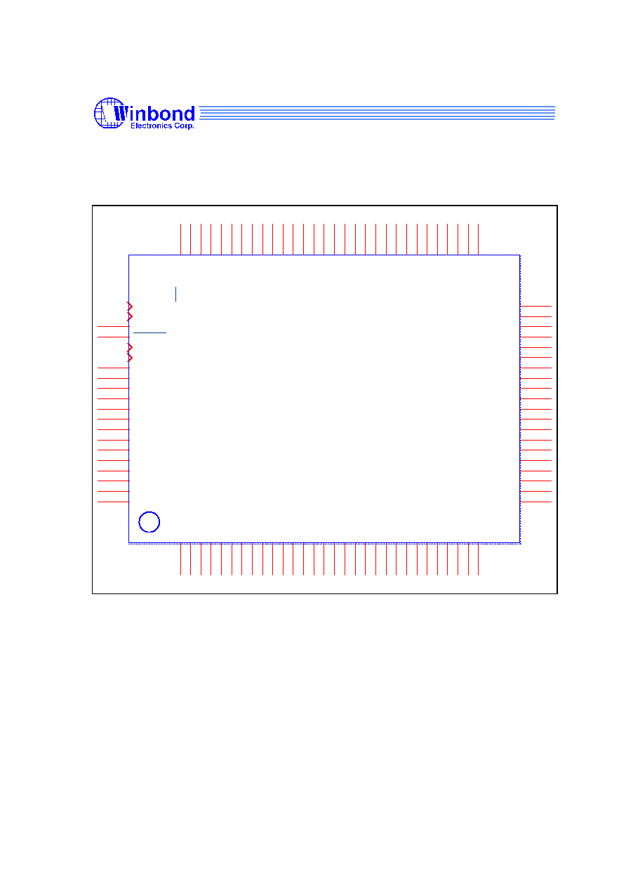
3 PIN CONFIGURATION
Figure 3-1 shows the pin assignment. The package type is 100pin QFP.
W925E/C240
BUZ
79
EA/DATA
80
TEST/MODE
78
P17
77
P16
76
P15
75
P14
74
P13
73
P12
72
P11
71
P10
70
P27
69
P26
68
P25
67
P24
66
P23
65
P22
64
P21
63
P20
62
P37
61
P36
60
P35
59
P34
58
P33
57
P32
56
P31
55
P30
54
P47
53
P46
52
P45
51
P44/VPOS
50
P43
49
P42/VNEG
48
P41
47
P40
46
DTMF/FSK
45
NC
42
NC
41
NC
30
NC
29
NC
28
NC
27
NC
26
NC
25
NC
24
NC
23
NC
22
NC
21
NC
20
NC
19
NC
18
NC
17
NC
16
NC
15
NC
14
NC
13
NC
12
NC
11
NC
10
NC
9
NC
8
NC
7
NC
6
NC
5
NC
4
NC
3
NC
2
NC
1
NC
100
NC
99
NC
98
NC
97
NC
96
INP2
40
INN2
39
GCFB2
38
VAS
37
VAD
36
GCFB1
35
INN1
34
INP1
33
VREF
32
CAP
31
RNGDI
44
RNGRC
43
P07
95
P06
94
P05
93
P04
92
P03
91
P02
90
P01
89
P00
88
VSS
87
XOUT1
86
XIN1
85
RESET/VPP
84
VDD
83
XIN2
82
XOUT2
81
Figure 3-1 W925E/C240 Pin Configuration
W925E/C240
8-bit CID Microcontroller
-6-
Release Date : 2002/7/2
Revision : A6
4 PIN DESCRIPTION
TEST/MODE I/O TEST pin. In E version, it works as a Mode pin to select programming
mode. In C version (Mask type), this pin with internal pull-low resistor.
EA
/DATA
I,I/O Set high for normal function. In E version, it works as a Data pin. In C
version, this pin with internal pull-high resistor.
RESET /VPP
I
RESET pin. A low pulse causes the whole chip reset. In E version, this
pin work as a VPP pin which is a supply programming voltage. In C
version, this pin with internal pull-high resistor.
RNGDI
I
Ring Detect Input (Schmitt trigger input). Used for ring detection and line
reversal detection. Must maintain a voltage between VAD and VAS.
RNGRC
O Ring RC (Open drain output and Schmitt trigger input). Used to set the
time interval from the end of RNGDI pin to the inactive condition of the
RNGON pin. An external resistor must connected to VAD and a capacitor
connected to VSS, the time interval is the RC time constant.
CAP
O
Must be connected 0.1
�
F capacitor to VSS.
VREF
O
Reference Voltage. Nominally, VDD/2 is used to bias the input of the gain
control op-amp.
GCFB1
O
Op-amp1 Feed-back Gain Control signal. Select the input gain by
connecting this pin and the INN1 pin with feed-back resistor. It is
recommended that the op-amp1 be set to unity gain.
INN1
I
Inverting Input of the gain control op-amp1.
INP1
I
Non-inverting Input of the gain control op-amp1.
GCFB2
O
Op-amp2 Feed-back Gain Control signal. Select the input gain by
connecting this pin and the INN2 pin with feed-back resistor. It is
recommended that the op-amp2 be set to unity gain.
INN2
I
Inverting Input of the gain control op-amp2.
INP2
I
Non-inverting Input of the gain control op-amp2.
VAD
I
Analog voltage supply.
VAS
I
Analog ground.
VDD
I
Digital voltage supply.
VSS
I
Digital ground.
XOUT1
O
Output pin for main-oscillator. Connected to 3.58MHz crystal for CID
function.
XIN1
I
Input pin for main-oscillator. Connected to 3.58MHz crystal for CID
function.
XOUT2
O
Output pin for sub-oscillator. Connected to 32.768KHz crystal only.
Suggest to add an external capacitor about 10~30pF to ground(VSS) for
the accuracy of the oscillator.
XIN2
I
Input pin for sub-oscillator. Connected to 32.768KHz crystal only. Suggest
to add an external capacitor about 10~30pF to ground(VSS) for the
accuracy of the oscillator.
DTMF/FSK
O
FTE=0, Dual-Tone Multi-Frequency(DTMF) signal output
FTE=1, FSK signal output

W925E/C240
8-bit CID Microcontroller
-7-
Release Date : 2002/7/2
Revision : A6
BUZ
O
Buzzer output pin. If buzzer function is disabled, BUZ pin is in floating state.
P00-P07
I/O Input/output port0. Port0 data can be bit controlled. The I/O mode is
controlled by P0IO register. Port0 is open drain type when it is configured
as output mode.
P10-P17
I/O Input/output port1 with pull high resistors. Port1 data can be bit controlled.
The I/O mode is controlled by P1IO register. The P10-P13 and P14-P17
indicate the external interrupt pins(INT2 and INT3)
P20-P27
I/O Input/output port2 with pull high resistors. Port2 data can be bit controlled.
The I/O mode is controlled by P2IO register.
P30-P37
I/O Input/output port3 with pull high resistors. Port3 data can be bit controlled.
The I/O mode is controlled by P3IO register. The special function of port3 is
referred to the description of P3 register.
P40-P47
I/O Contents are byte controlled. Pull high and I/O mode can be bit controlled.
The special function of P4 is referred to the description of P4 register.
VPOS,
VNEG
I
The comparator V+, V- analog input pins. Share pin with P4.2 and P4.4

W925E/C240
8-bit CID Microcontroller
-8-
Release Date : 2002/7/2
Revision : A6
5 BLOCK DIAGRAM
FSK,CAS
(W91030)
RNGDI
RNGRC
INP2
INN2
GCFB2
VREF
CAP
8-bit
�
C
CIDE
FSKE
CASE
S/P
DCLK
DATA
FD7~FD0
RNG
ALGO
FDR
FCD
DTMF
RECEIVER
DTMFH
DTMFL
DD3~DD0
P0
8
P1
8
P2
8
P3
8
P4
8
X
I
N
1
X
O
U
T
1
X
I
N
2
X
O
U
T
2
V
D
D
V
S
S
V
A
D
V
A
S
Internal CID and uC interface signal
FDATA
D-latch
DTMFD
RNGF
ALGOF
FDRF
DTMFDF
Fosc
CASH,CASL
INP1
INN1
GCFB1
CASPT
CASAT
DTMFPT
DTMFAT
ck
R
E
S
E
T
/
V
P
P
E
A
/
D
A
T
A
DTMFE
B
U
Z
D
T
M
F
/
F
S
K
TEST/MODE
RST
F
M
DCLK
FSK
modulator
FSF

W925E/C240
8-bit CID Microcontroller
-9-
Release Date : 2002/7/2
Revision : A6
6 FUNCTIONAL DESCRIPTION
The W925E/C240 is an 8-bit micro-controller with CID function. The 8-bit micro-control has the
same instruction set as the 8051 family, with one addition: DEC DPTR (op-code A5H, the DPTR
is decreased by 1). In addition, the W925E/C240 contains on-chip 8K bytes MOVX RAM.
ROM:
There are 256K bytes EEPROM/MASK ROM. Only 128K bytes EEPROM/MASK ROM is used for
program code. The completely 256K bytes EEPROM/MASK ROM can be used for the look-up
table memory.
On-chip Data RAM:
The W925E/C240 has 8K normal RAM which address is from 0000H to 1FFFH. It only can be
accessed by MOVX instruction; this on-chip RAM is optional under software control. The on-chip
data RAM is not used for executable program memory. There is no conflict or overlap among the
256 bytes scratchpad RAM and the 8K Bytes MOVX RAM as they use different addressing
modes and separate instructions.
CID:
The CID functions include the FSK decoder, CAS detector, DTMF decoder and ring detector.
FSK modulator:
Support ITU-T V.23 and Bellcore 202 FSK transmit modulated signal.
DTMF modulator:
The W925E/C240 built-in dual tone multi-frequency generator.
I/O Ports:
The W925E/C240 has five 8-bit I/O ports giving a total of 40 lines. Port0 to Port3 can be used as
an 8-bit general I/O port with bit-addressable. The I/O mode of each port is controlled by PxIO
registers. Port1 to Port4 have internal pull high resistors enabled/disabled by PxH registers. Port0
is open-drain type in output mode.
Serial I/O port:
The serial port, through P4.0 (SCLK) and P4.1 (SDATA), is an 8-bit synchronous serial I/O
interface.
Timers:
The W925E/C240 has two 13/16-bit timers or 8 bits auto-reload timers. An independent watchdog
timer is used as a system monitor or as a very long time period timer. A divider can produce the
divider interrupt in every period of 0.5S or 0.25S.
Comparator:
The W925E/C240 has an internal comparator with one external analog signal input path VNEG
and an external path VPOS or a regulator voltage for the reference input REF1.
Interrupts:
The W925E/C240 provides eleven interrupt resources with two priority level, including 4 external
interrupt sources, 2 timer interrupts, 1 CID interrupt, 1 divider interrupt, 1 serial port interrupt, 1
comparator interrupt and 1 watchdog timer interrupt.
Power Management:
The W925E/C240 has IDLE and POWER DOWN modes of operation. In the IDLE mode, the
clock to the CPU core is stopped however the functions of the timers, divider, CID and interrupts
are active continuously. In the POWER DOWN mode, both of the system clock stop oscillating
and the chip operation is completely stopped. POWER DOWN mode is the state of the lowest
power consumption.
W925E/C240
8-bit CID Microcontroller
-10-
Release Date : 2002/7/2
Revision : A6
6.1 Memory Organization
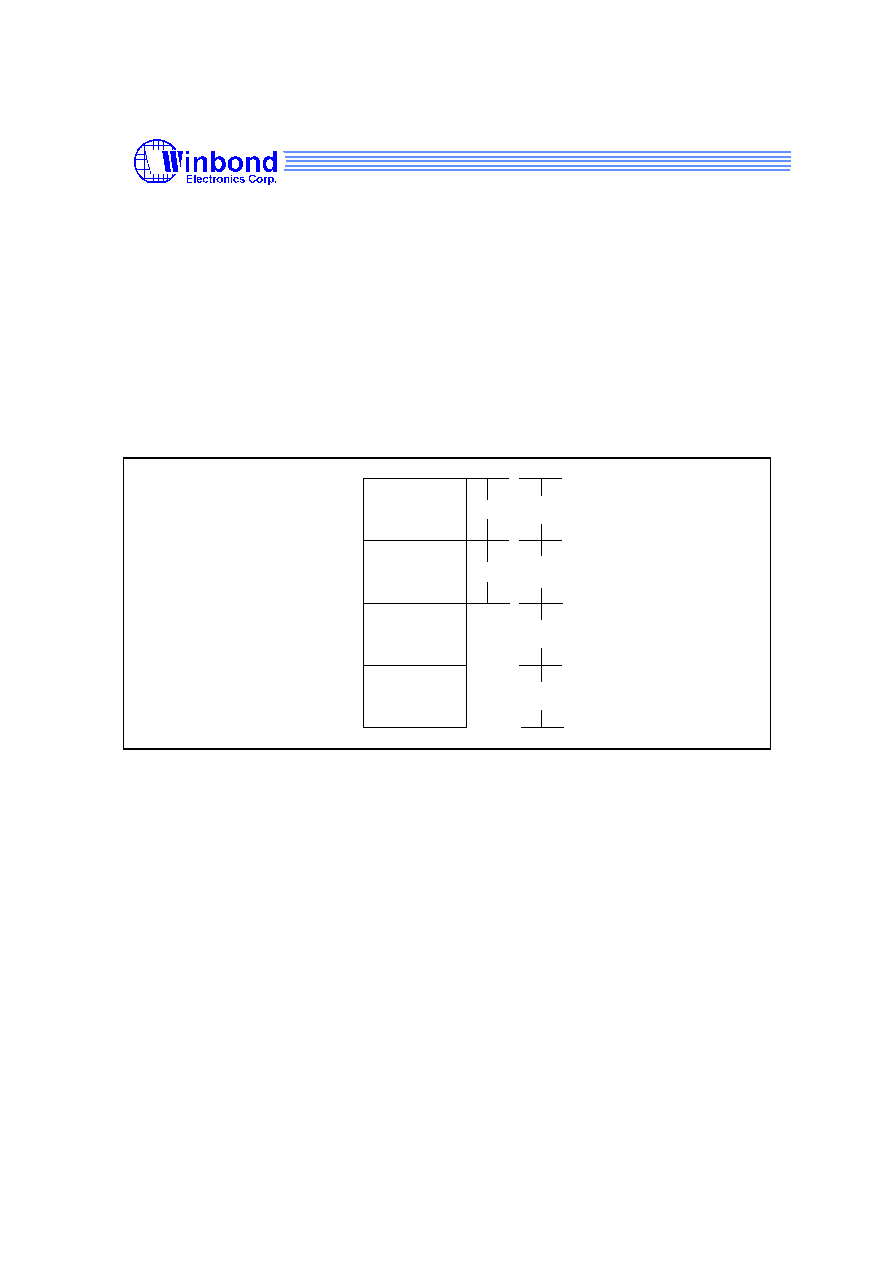
The W925E/C240 separates the memory into two separate sections, the Program Memory and
the Data Memory. The Program Memory is used to store the instruction op-codes and look-up
table data, while the Data Memory is used to store data or for memory mapped devices.
Program Memory:
The Program Memory on the W925E/C240 can be up to 256K bytes that are divided into 4 pages,
each page has the size of 64K bytes. The upper 128K bytes are used to store the op-codes and
the whole 256K can be used to store look-up table data. Because the op-code is 64K
addressable, a PG bit in PAGE register decides which ROM page between page0 and page1 is
enabled and the ALU fetches the op-code from the selected ROM page. If PG=0, ALU fetches the
op-code from page0. If PG=1, ALU fetches the op-code from page1.
When MOVC instruction is
executed, ALU fetches the look-up table data according the indication of LT1 and LT0 bits. The
value of LT1 and LT0 indicates which ROM page is active for look-up table instruction.
64K
Page0
64K
Page3
64K
Page2
64K
Page1
3FFFF
0FFFF
1FFFF
2FFFF
30000
00000
10000
20000
PG=0
PG=1
LT1,0
=00
LT1,0
=01
LT1,0
=10
LT1,0
=11
Figure 6-1 Program Memory Map
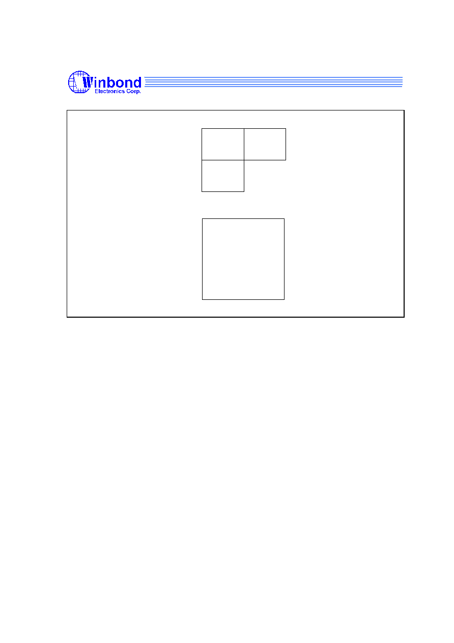
Data Memory:
The W925E/C240 contains on-chip 8K MOVX RAM of Data Memory, which can only be accessed
by MOVX instructions from the address 0000H to 1FFFH. In addition, the W925E/C240 has 256
bytes of on-chip scratchpad RAM. This can be accessed either by direct addressing or by indirect
addressing. There are also Special Function Registers (SFRs), which can only be accessed by
direct addressing. Since the scratchpad RAM is only 256 bytes, it can be used only when data
contents are small. In the event that larger data contents are present, the only one selection is
on-chip MOVX RAM. The on-chip MOVX RAM can only be accessed by a MOVX instruction.
However, the on-chip RAM has the fastest access times. The memory map is shown Figure 6-2
and Figure 6-3 shows the scratched-pad RAM/register addressing.
W925E/C240
8-bit CID Microcontroller
-11-
Release Date : 2002/7/2
Revision : A6
8K byte SRAM On chip
0000H
1FFFH
Indirect
Addressing
RAM
Direct &
Indirect
Addressing
RAM
SFRs Direct
Addressing
only
7FH
00H
FFH
80H
Figure 6-2 memory map
W925E/C240
8-bit CID Microcontroller
-12-
Release Date : 2002/7/2
Revision : A6
FFh
80h
7Fh
30h
2Fh
2Eh
2Dh
2Ch
2Bh
2Ah
29h
28h
27h
26h
25h
24h
23h
22h
21h
20h
1Fh
18h
17h
10h
0Fh
08h
07h
00h
78
79
7A
7B
7C
7D
7E
7F
70
71
72
73
74
75
76
77
68
69
6A
6B
6C
6D
6E
6F
60
61
62
63
64
65
66
67
58
59
5A
5B
5C
50
51
52
53
54
5D
5E
5F
55
56
57
48
49
4A
4B
4C
4D
4E
4F
40
41
42
43
44
45
46
47
38
39
3A
3B
3C
3D
3E
3F
30
31
32
33
34
35
36
37
28
29
2A
2B
2C
2D
2E
2F
20
21
22
23
24
25
26
27
18
19
1A
1B
1C
1D
1E
1F
10
11
12
13
14
15
16
17
08
09
0A
0B
0C
0D
0E
0F
00
01
02
03
04
05
06
07
Indirect RAM
Direct RAM
Bank 3
Bank 2
Bank 1
Bank 0
Bit Addressable
20H- 2FH
Figure 6-3 Scratchpad RAM/Register Addressing
W925E/C240
8-bit CID Microcontroller
-13-
Release Date : 2002/7/2
Revision : A6
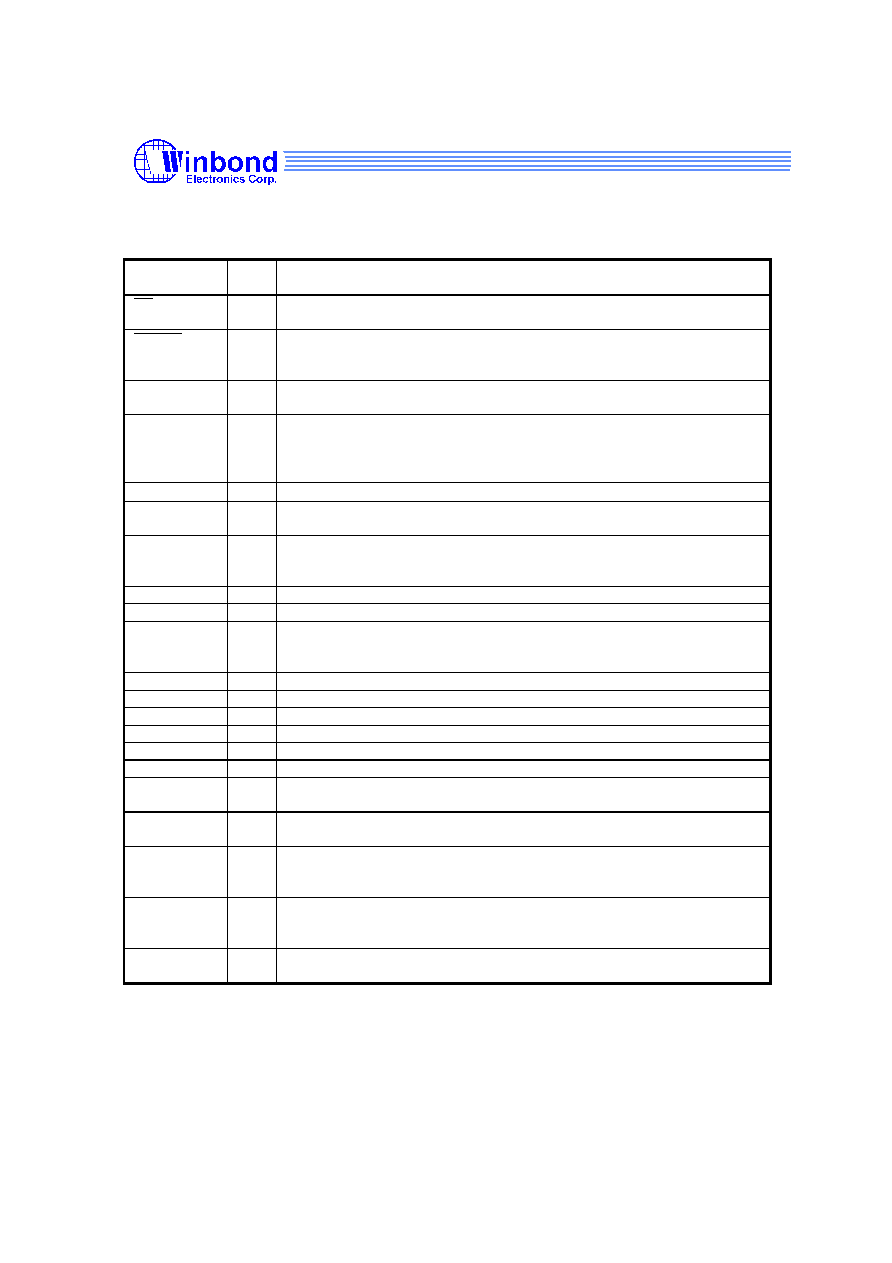
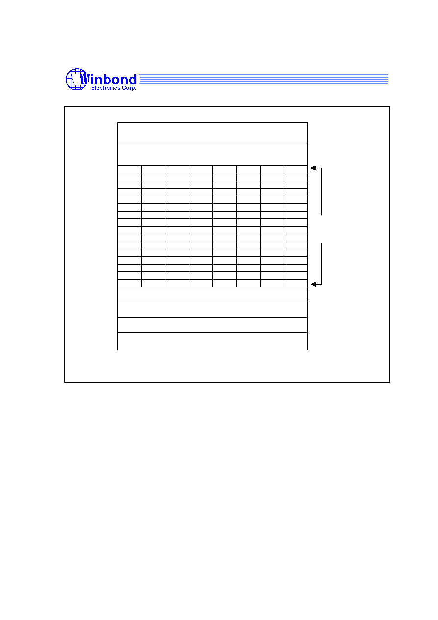
6.2 Special Function Registers
The W925E/C240 uses Special Function Registers (SFRs) to control and monitor peripherals and
their Modes.
The SFRs reside in the register locations 80-FFh and are accessed by direct addressing only.
Some of the SFRs are bit addressable. This is very useful in cases where one wishes to modify a
particular bit without changing the others. The SFRs that are bit addressable are those whose
addresses end in 0 or 8. The list of SFRs is as follows. The table is condensed with eight
locations per row. Empty locations indicate that there are no registers at these addresses. The
content of reserved bits or registers is not guaranteed.
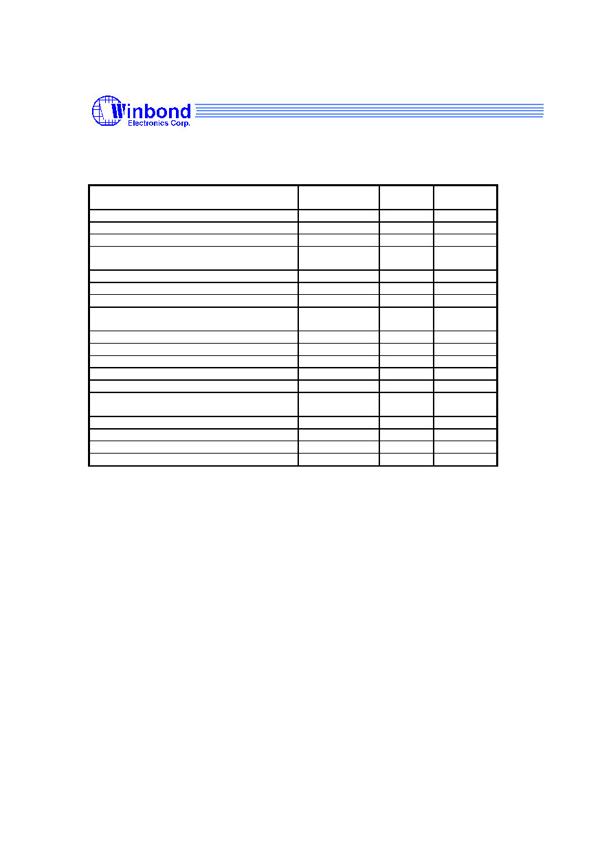
Table 1 Special Function Register Location Table
F8 EIP
CIDGD
CIDGA
F0 B
E8 EIE
E0 ACC
D8 WDCON
D0 PSW
C8 DIVC
C0 SCON1
SBUF1
REGVC
PMR
STATUS FSKTC
FSKTB
B8 IP
DTMFG COMPR IRC1
IRC2
CASPT
CASAT
B0 P3
CIDR
CIDFG
CIDPCR FSKDR
DTMFDR DTMFPT DTMFAT
A8 IE
P4IO
A0 P2
HB
P4H
P4
98
P1EF
P1H
P2H
P3H
90 P1
EXIF
RPAGE
P1SR
P0IO
P1IO
P2IO
P3IO
88 TCON
TMOD
TL0
TL1
TH0
TH1
CKCON1 CKCON2
80 P0
SP
DPL
DPH
DPL1
DPH1
DPS
PCON
Note: The SFRs in the column with dark borders are bit-addressable.
A brief description of the SFRs now follows.
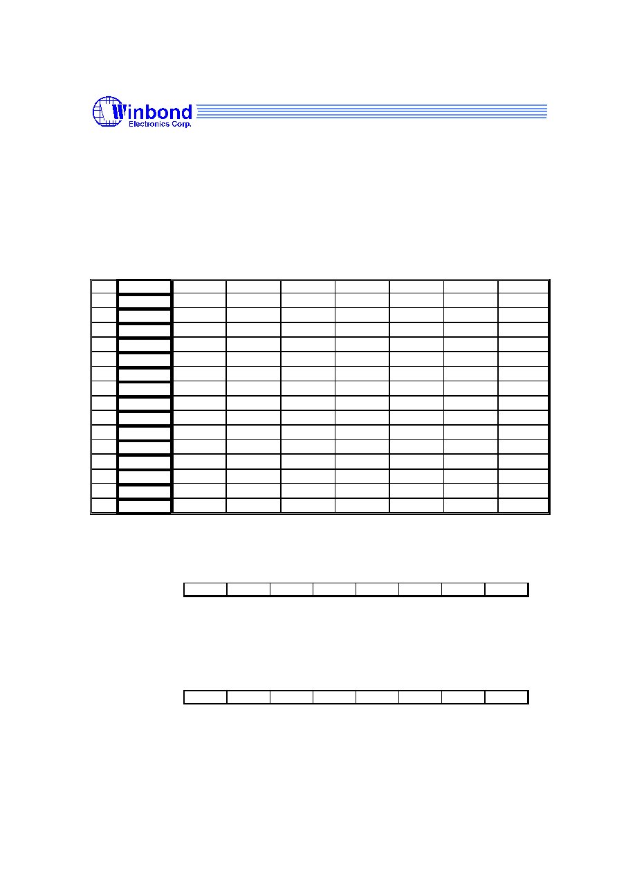
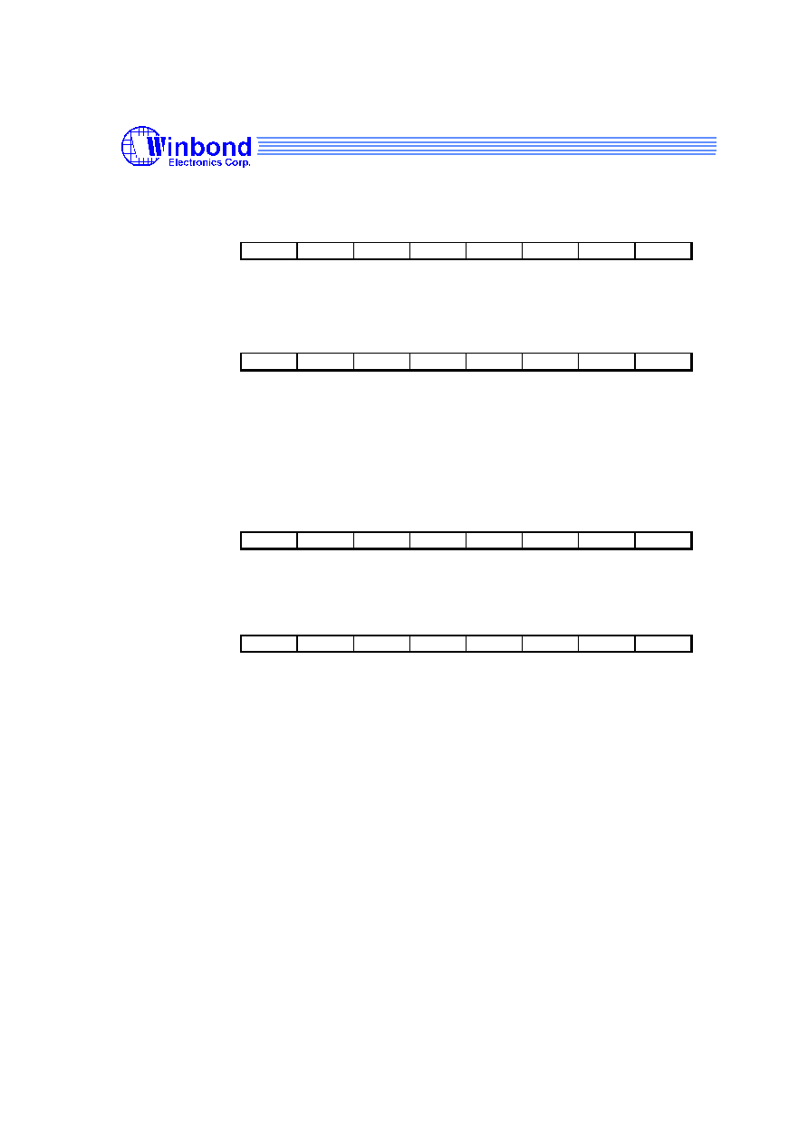
PORT 0 (initial=FFh, input mode)
Bit:
7
6
5
4
3
2
1
0
P0.7
P0.6
P0.5
P0.4
P0.3
P0.2
P0.1
P0.0
Mnemonic: P0 Address: 80h
P0: P0 can be selected as input or output mode by the P0IO register. At initial reset, P0IO is
set to FFH, P0 is used as input mode. When P0IO is set to 0, the P0 is used as CMOS
open drain mode.
STACK POINTER (initial=07H)
Bit:
7
6
5
4
3
2
1
0
SP.7
SP.6
SP.5
SP.4
SP.3
SP.2
SP.1
SP.0
Mnemonic: SP Address: 81h
SP: The Stack Pointer stores the scratchpad RAM address where the stack begins. In other
words, it always points to the top of the stack.

W925E/C240
8-bit CID Microcontroller
-14-
Release Date : 2002/7/2
Revision : A6
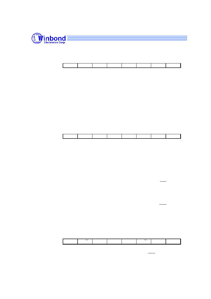
DATA POINTER LOW (initial=00H)
Bit:
7
6
5
4
3
2
1
0
DPL.7 DPL.6 DPL.5 DPL.4 DPL.3 DPL.2 DPL.1 DPL.0
Mnemonic: DPL Address: 82h
DPL: This is the low byte of the standard 8052 16-bit data pointer.
DATA POINTER HIGH (initial=00H)
Bit:
7
6
5
4
3
2
1
0
DPH.7 DPH.6 DPH.5 DPH.4 DPH.3 DPH.2 DPH.1 DPH.0
Mnemonic: DPH Address: 83h
DPH: This is the high byte of the standard 8052 16-bit data pointer.
DATA POINTER LOW1 (initial=00H)
Bit:
7
6
5
4
3
2
1
0
DPL1.7 DPL1.6 DPL1.5 DPL1.4 DPL1.3 DPL1.2 DPL1.1 DPL1.0
Mnemonic: DPL1 Address: 84h
DPL1: This is the low byte of the new additional 16-bit data pointer that has been added to the
W925E/C240. The user can switch between DPL, DPH and DPL1, DPH1 simply by
setting register DPS.0 = 1. The instructions that use DPTR will now access DPL1 and
DPH1 in place of DPL and DPH. If they are not required they can be used as
conventional register locations by the user.
DATA POINTER HIGH1 (initial=00H)
Bit:
7
6
5
4
3
2
1
0
DPH1.7 DPH1.6 DPH1.5 DPH1.4 DPH1.3 DPH1.2 DPH1.1 DPH1.0
Mnemonic: DPH1 Address: 85h
DPH1: This is the high byte of the new additional 16-bit data pointer that has been added to the
W925E/C240. The user can switch between DPL, DPH and DPL1, DPH1 simply by
setting register DPS = 1. The instructions that use DPTR will now access DPL1 and
DPH1 in place of DPL and DPH. If they are not required they can be used as
conventional register locations by the user.
DATA POINTER SELECT (initial=00H)
Bit:
7
6
5
4
3
2
1
0
-
-
-
-
-
-
-
DPS.0
Mnemonic: DPS Address: 86h
DPS.0: This bit is used to select either the DPL,DPH pair or the DPL1,DPH1 pair as the active
Data Pointer. When set to 1, DPL1,DPH1 will be selected, otherwise DPL,DPH will be
selected.
DPS.1-7:These bits are reserved, but will read 0.
W925E/C240
8-bit CID Microcontroller
-15-
Release Date : 2002/7/2
Revision : A6
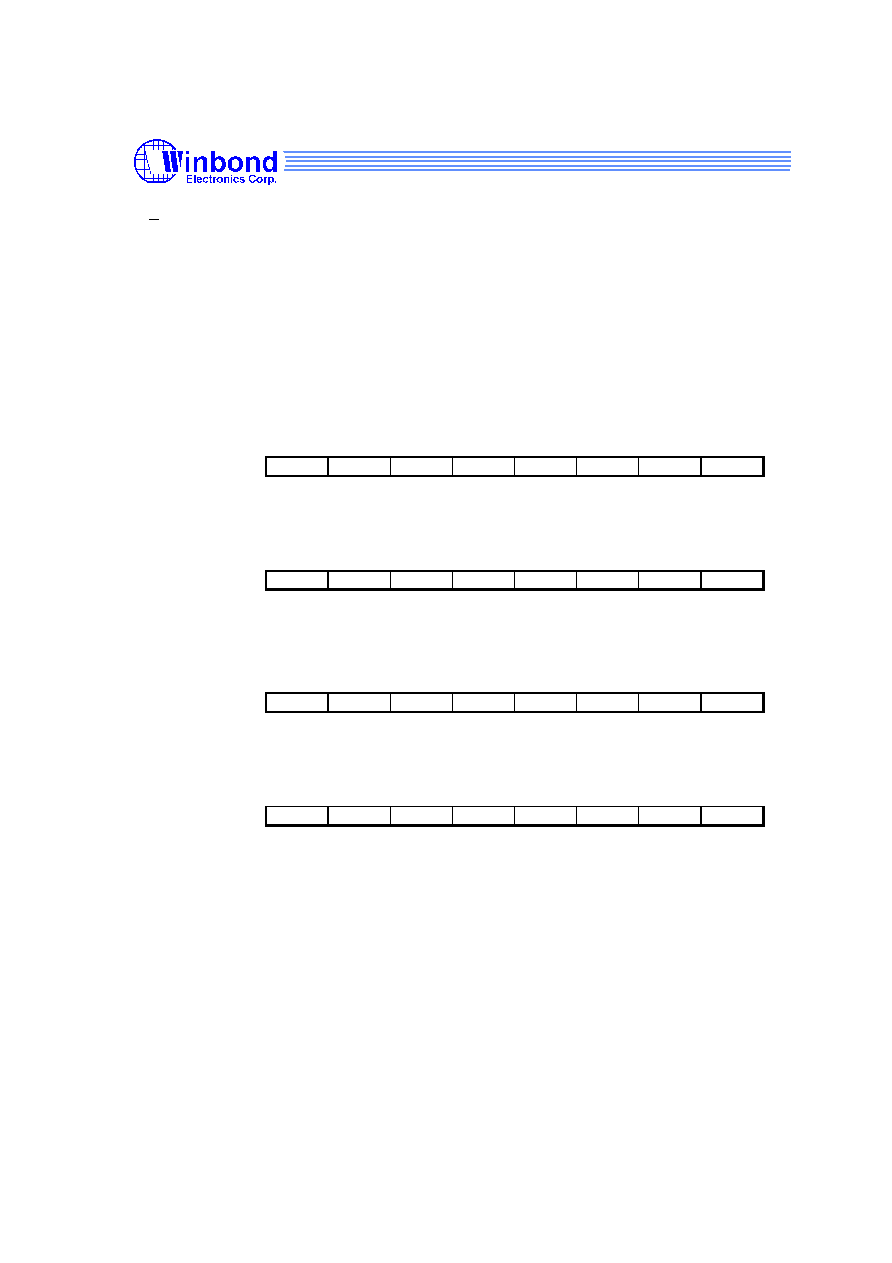
POWER CONTROL (initial=00H)
Bit:
7
6
5
4
3
2
1
0
-
-
-
IDLT
GF1
GF0
PD
IDL
Mnemonic: PCON Address: 87h
IDLT: This bit controls the idle mode type. In idle mode when idle mode is released by any
interrupt, if IDLT=1 it will not jump to the corresponding interrupt; if IDLT=0 it will jump to
the corresponding interrupt.
GF1-0: These two bits are general purpose user flags.
PD: Setting this bit causes the W925E/C240 to go into the POWER DOWN mode. In this
mode all the clocks are stopped and program execution is frozen. Power down mode
can be released by INT0~INT3 and ring detection of CID interrupt.
IDL: Setting this bit causes the W925E/C240 to go into the IDLE mode. The type of idle
mode is selected by IDLT. In this mode the clocks to the CPU are stopped, so program
execution is frozen. But the clock path to the timers blocks and interrupt blocks is not
stopped, and these blocks continue operating.
TIMER CONTROL (initial=00H)
Bit:
7
6
5
4
3
2
1
0
TF1
TR1
TF0
TR0
IE1
IT1
IE0
IT0
Mnemonic: TCON Address: 88h
TF1: Timer 1 overflow flag. This bit is set when Timer 1 overflows. It is cleared automatically
when the program does a timer 1 interrupt service routine. Software can also set or clear
this bit.
TR1: Timer 1 run control. This bit is set or cleared by software to turn timer on or off.
TF0: Timer 0 overflow flag. This bit is set when Timer 0 overflows. It is cleared automatically
when the program does a timer 0 interrupt service routine. Software can also set or clear
this bit.
TR0: Timer 0 run control. This bit is set or cleared by software to turn timer on or off.
IE1: Interrupt 1 edge detect: Set by hardware when an edge/level is detected on INT1. This bit
is cleared by hardware when the service routine is vectored to only if the interrupt was
edge triggered. Otherwise it follows the pin.
IT1: Interrupt 1 type control: Set/cleared by software to specify falling edge/ low level triggered
external inputs.
IE0: Interrupt 0 edge detect: Set by hardware when an edge/level is detected on INT0 . This bit
is cleared by hardware when the service routine is vectored to only if the interrupt was
edge triggered. Otherwise it follows the pin.
IT0: Interrupt 0 type control. Set/cleared by software to specify falling edge/ low level triggered
external inputs.
TIMER MODE CONTROL (initial=00H)
Bit:
7
6
5
4
3
2
1
0
GATE
C/ T
M1
M0
GATE
C/ T
M1
M0
Mnemonic: TMOD Address: 89h
Bit7~4 control timer 1, bit3~0 control timer0
GATE: Gating control. When this bit is set, Timer x is enabled only while INTx pin is high and
TRx control bit is set. When cleared, Timer x is enabled whenever TRx control bit is set.
W925E/C240
8-bit CID Microcontroller
-16-
Release Date : 2002/7/2
Revision : A6
C/ T : Timer or Counter Select. When cleared, the timer is incremented by internal clocks. When
set, the timer counts high-to-low edges of the Tx pin.
Note: X is either 0 or 1.
M1, M0: Mode Select bits:
M1 M0 Mode
0
0
Mode 0: 13-bits timer
0
1
Mode 1: 16-bits timer
1
0
Mode 2: 8-bits with auto-reload from Thx
1
1
Reserved
TIMER 0 LOW BYTE (initial=00H)
Bit:
7
6
5
4
3
2
1
0
TL0.7 TL0.6 TL0.5 TL0.4 TL0.3 TL0.2 TL0.1 TL0.0
Mnemonic: TL0 Address: 8Ah
TL0.7-0: Timer 0 low byte register.
TIMER 1 LOW BYTE (initial=00H)
Bit:
7
6
5
4
3
2
1
0
TL1.7 TL1.6 TL1.5 TL1.4 TL1.3 TL1.2 TL1.1 TL1.0
Mnemonic: TL1 Address: 8Bh
TL1.7-0: Timer 1 low byte register.
TIMER 0 HIGH BYTE (initial=00H)
Bit:
7
6
5
4
3
2
1
0
TH0.7 TH0.6 TH0.5 TH0.4 TH0.3 TH0.2 TH0.1 TH0.0
Mnemonic: TH0 Address: 8Ch
TH0.7-0: Timer 0 high byte register.
TIMER 1 HIGH BYTE (initial=00H)
Bit:
7
6
5
4
3
2
1
0
TH1.7 TH1.6 TH1.5 TH1.4 TH1.3 TH1.2 TH1.1 TH1.0
Mnemonic: TH1 Address: 8Dh
TH1.7-0: Timer 1 high byte register.

W925E/C240
8-bit CID Microcontroller
-17-
Release Date : 2002/7/2
Revision : A6
CLOCK CONTROL1 (initial=00H)
Bit:
7
6
5
4
3
2
1
0
WD1
WD0
T1S1 T1S0 T0S1 T0S0
DIVS
M
/S
Mnemonic: CKCON1 Address: 8Eh
WD1-0: Watchdog timer mode select bits: These bits determine the time-out period for the
watchdog timer. In all four time-out options the reset time-out is 512 clocks more than the
interrupt time-out period.
WD1 WD0 Interrupt time-out
Reset time-out
0
0
Fosc/2
12
Fosc/2
12
+ 512
0
1
Fosc/2
15
Fosc/2
15
+ 512
1
0
Fosc/2
18
Fosc/2
18
+ 512
1
1
Fosc/2
21
Fosc/2
21
+ 512
T0S0-1&T1S0-1: Timer0 & Timer1 clock source mode select bits. These bits determine the timer0
& timer1 clock source.
T0S1
(T1S1)
T0S0
(T1S0)
Prescale clock
source
0
0
Fosc/2
2
0
1
Fosc/2
6
1
0
Fosc/2
10
1
1
Fs
DIVS: Divider clock source control bit 1:
DIVS = 0 : Fs/2
13
DIVS= 1 : Fs/2
14
M /S: System clock source control bit :
M /S = 0 : Fosc = XIN1 ( F
M
)
M /S = 1 : Fosc = XIN2 ( Fs)
CLOCK CONTROL2 (initial=00H)
Bit:
7
6
5
4
3
2
1
0
ENBUZ BUZSL KT1
KT0
-
-
-
-
Mnemonic: CKCON2 Address: 8Fh
ENBUZ: When ENBUZ=1 the BUZ pin works as buzzer output, otherwise BUZ pin is in floating
state.
BUZSL: Buzzer output selection. When BUZSL=0 BUZ is the output of octave tone. When
BUZZL=1, BUZ is the output of key tone.
KT1-0: Key tone frequency sources from divider. When divider is enable, KT1 and KT0
determines the key tone frequency.
KT1 KT0
key tone
frequency
0
0
Low
0
1
512Hz
1
0
1024Hz
1
1
2048Hz
PORT 1 (initial=FFh, input mode)
Bit:
7
6
5
4
3
2
1
0
P1.7 P1.6
P1.5
P1.4
P1.3
P1.2
P1.1
P1.0
W925E/C240
8-bit CID Microcontroller
-18-
Release Date : 2002/7/2
Revision : A6
Mnemonic: P1 Address: 90h
P1.7-0: P1 can be selected as input or output mode by the P1IO register , At initial reset , P1IO is
set to 1, so P1 is used as input mode . When P1IO is set to 0 , the P1 is used as
CMOS output mode . When P1EF are set and P1IO are set as input mode , P1 can be
used as external interrupt source. The functions are listed below .
P1.0 : INT2.0 External Interrupt 2
P1.1 : INT2.1 External Interrupt 2
P1.2 : INT2.2 External Interrupt 2
P1.3 : INT2.3 External Interrupt 2
P1.4 : INT3.0 External Interrupt 3
P1.5 : INT3.1 External Interrupt 3
P1.6 : INT3.2 External Interrupt 3
P1.7 : INT3.3 External Interrupt 3
EXTERNAL INTERRUPT FLAG (initial=00H)
Bit:
7
6
5
4
3
2
1
0
-
-
-
COMPF DIVF
CIDF
IE3
IE2
Mnemonic: EXIF Address: 91h
COMPF: Comparator flag. Set by hardware when RESC bit is from low to high.
DIVF: Divider overflow flag.
CIDF: CID interrupt flag. Set by hardware when at least one of CID flags is set.
IE3: External Interrupt 3 flag. Set by hardware when a falling edge is detected on INT3.
IE2: External Interrupt 2 flag. Set by hardware when a falling edge is detected on INT2.
ROM PAGE POINTER (initial=00H)
Bit:
7
6
5
4
3
2
1
0
-
-
LT1
LT0
-
-
-
PG
Mnemonic: RPAGE Address: 92h
LT1 and LT0 determine the ROM page of the instruction MOVC reading the content from ROM.
ROM PAGE Rom address
(LT1,LT0) = (0, 0)
Page 0
00000H-0FFFFH
(LT1,LT0) = (0, 1)
Page 1
10000H-1FFFFH
(LT1,LT0) = (1, 0)
Page 2
20000H-2FFFFH
(LT1,LT0) = (1, 1)
Page 3
30000H-3FFFFH
PG = 0 indicates the executing program is in page 0, from 00000H-0FFFFH
PG = 1 indicates the executing program is in page 1, from 10000H-1FFFFH
P1 PINS STATUS (initial=00H)
Bit:
7
6
5
4
3
2
1
0
P1.7SR P1.6SR P1.5SR P1.4SR P1.3SR P1.2SR P1.1SR P1.0SR
Mnemonic: P1SR Address: 93h
P1SR: Set when a falling edge is detected on the corresponding P1 pin, clear by software.
W925E/C240
8-bit CID Microcontroller
-19-
Release Date : 2002/7/2
Revision : A6
P0 I/O PORT CONTROL (initial=FFH)
Bit:
7
6
5
4
3
2
1
0
P0.7IO P0.6IO P0.5IO P0.4IO P0.3IO P0.2IO P0.1IO P0.0IO
Mnemonic: P0IO Address: 94h
P0IO: P0 pins I/O control.
1: input mode
0: output mode
P1 I/O PORT CONTROL (initial=FFH)
Bit:
7
6
5
4
3
2
1
0
P1.7IO P1.6IO P1.5IO P1.4IO P1.3IO P1.2IO P1.1IO P1.0IO
Mnemonic: P1IO Address: 95h
P1IO: P1 pins I/O control.
1: input mode
0: output mode
P2 I/O PORT CONTROL (initial=FFH)
Bit:
7
6
5
4
3
2
1
0
P2.7IO P2.6IO P2.5IO P2.4IO P2.3IO P2.2IO P2.1IO P2.0IO
Mnemonic: P2IO Address: 96h
P2IO: P2 pins I/O control.
1: input mode
0: output mode
P3 I/O PORT CONTROL (initial=FFH)
Bit:
7
6
5
4
3
2
1
0
P3.7IO P3.6IO P3.5IO P3.4IO P3.3IO P3.2IO P3.1IO P3.0IO
Mnemonic: P3IO Address: 97h
P3IO: P3 pins I/O control.
1: input mode
0: output mode
P1 PINS INTERRUPT EABLE (initial=00H)
Bit:
7
6
5
4
3
2
1
0
P1.7EF P1.6EF P1.5EF P1.4EF P1.3EF P1.2EF P1.1EF P1.0EF
Mnemonic: P1EF Address: 9Bh
P1EF: P1 pins interrupt function enabled/disabled register
0: disable
1: enable
P1 PULL-HIGH CONTROL (initial=00H)
Bit:
7
6
5
4
3
2
1
0
P1.7H P1.6H P1.5H P1.4H P1.3H P1.2H P1.1H P1.0H
Mnemonic: P1H Address: 9Dh
P1H: Port1 pins pull-high resistor enable/disable
1: enable
0: disable

W925E/C240
8-bit CID Microcontroller
-20-
Release Date : 2002/7/2
Revision : A6
P2 PULL-HIGH CONTROL (initial=00H)
Bit:
7
6
5
4
3
2
1
0
P2.7H P2.6H P2.5H P2.4H P2.3H P2.2H P2.1H P2.0H
Mnemonic: P2H Address: 9Eh
P2H: Port1 pins pull-high resistor enable/disable
1: enable
0: disable
P3 PULL-HIGH CONTROL (initial=00H)
Bit:
7
6
5
4
3
2
1
0
P3.7H P3.6H P3.5H P3.4H P3.3H P3.2H P3.1H P3.0H
Mnemonic: P3H Address: 9Fh
P3H: Port1 pins pull-high resistor enable/disable
1: enable
0: disable
PORT 2 (initial=FFh, input mode)
Bit:
7
6
5
4
3
2
1
0
P2.7
P2.6
P2.5
P2.4
P2.3
P2.2
P2.1
P2.0
Mnemonic: P2 Address: A0h
P2.7-0: Port 2 is a I/O port with internal pull-high resistor. P2 can be selected as input or output
mode by the P2IO register. At initial reset, P2 is used as input mode. When P2IO is set to
0, P2 is used as CMOS output mode.
HIGH BYTE REGISTER (initial=00H)
Bit:
7
6
5
4
3
2
1
0
HB.7 HB.6 HB.5 HB.4 HB.3 HB.2 HB.1 HB.0
Mnemonic: HB Address: A1h
This register contains the high byte address during execution of " MOVX @Ri, " instructions.
P4 PULL-HIGH CONTROL (initial=00H)
Bit:
7
6
5
4
3
2
1
0
P4.7H P4.6H P4.5H P4.4H P4.3H P4.2H P4.1H P4.0H
Mnemonic: P4H Address: A2h
P4H: Port4 pins pull-high resistor enable/disable
1: enable
0: disable
PORT 4 (initial=FFh, input mode)
Bit:
7
6
5
4
3
2
1
0
P4.7
P4.6
P4.5
P4.4
P4.3
P4.2
P4.1
P4.0
Mnemonic: P4 Address: A6h
P4.7-0: Port 4 is a I/O port with internal pull-high resistor. P4 can be selected as input or output
mode by the P4IO register, At initial reset, P4IO is set to 0FFh, P4 is used as input
mode. When P4IO is set to 00h, P4 is used as CMOS output mode. Special function of
P4 is described below.
W925E/C240
8-bit CID Microcontroller
-21-
Release Date : 2002/7/2
Revision : A6
P4.7-5
I/O
Normal I/O
P4.4
VPOS
Positive input of the comparator
P4.2
VNEG
Negative input of the comparator
P4.1
SDATA
Serial port data I/O
P4.0
SCLK
Serial port clock I/O with Smith trigger in input path
INTERRUPT ENABLE (initial=00H)
Bit:
7
6
5
4
3
2
1
0
EA
ES1
-
-
ET1
EX1
ET0
EX0
Mnemonic: IE Address: A8h
EA: Global enable. Enable/disable all interrupts.
ES1: Enable Serial port interrupt
ET1: Enable Timer 1 interrupt
EX1: Enable external interrupt 1
ET0: Enable Timer 0 interrupt
EX0: Enable external interrupt 0
P4 I/O PORT CONTROL (initial=FFH)
Bit:
7
6
5
4
3
2
1
0
P4.7IO P4.6IO P4.5IO P4.4IO P4.3IO P4.2IO P4.1IO P4.0IO
Mnemonic: P4IO Address: AEh
P4IO: P4 pins I/O control.
1: input mode
0: output mode
PORT 3 (initial=FFh, input mode)
Bit:
7
6
5
4
3
2
1
0
P3.7
P3.6
P3.5
P3.4
P3.3
P3.2
P3.1
P3.0
Mnemonic: P3 Address: B0h
P3.7-0: P3 can be selected as input or output mode by the P3IO register, At initial reset, P3IO is
set to 0FFH, P3 is used as input mode. When P3IO is set to 00h, the P3 is used as
CMOS output mode. Special function of P3 is described below.
P3.5
T1
Timer/Counter 1 external count input
P3.4
T0
Timer/Counter 0 external count input
P3.3
INT1
External interrupt 1
P3.2
INT0
External interrupt 0
CID REGISTER (initial=00H,read only)
Bit:
7
6
5
4
3
2
1
0
-
FCLK FDATA FCD DTMFD FDR ALGO RNG
Mnemonic: CIDR Address: B1h
This SFR indicates the CID signal immediately. Register data is set or cleared by hardware only.
FCLK: FSK serial clock with the baud rate of 1200Hz.
FDATA: FSK serial bit data.
FCD: Set when FSK carrier is detected. Cleared when FSK carrier is disappeared.
DTMFD: Set when DTMF decoded data is ready. Cleared when DTMF signal ends.
FDR: Set when FSK 8 bits data is ready. Cleared before next FSK start bit comes

W925E/C240
8-bit CID Microcontroller
-22-
Release Date : 2002/7/2
Revision : A6
ALGO: Dual tone Alert signal Guard time detect signal. Set when a guard time qualified dual tone
alert signal has been detected. Cleared when the guard time qualified dual tone alert
signal is absent.
RNG: Ring detection bit. High to indicate the detection of line reversal and/or ringing.
CID FLAG GENERATOR (initial=00H)
Bit:
7
6
5
4
3
2
1
0
-
-
-
FSF DTMFDF FDRF ALGOF RNGF
Mnemonic: CIDFG Address: B2h
FSF: Set when FSK Latch clock low to high. Cleared by software
DTMFDF: Set when DTMFD low to high. Cleared by software
FDRF: Set when FDR low to high. Cleared by software.
ALGOF: Set when ALGO low to high. Cleared by software.
RNGF: Set when RNG low to high. Cleared by software.
CID POWER CONTROL REGISTER (initial=00H)
Bit:
7
6
5
4
3
2
1
0
-
-
-
CIDE
-
FSKE CASE DTMFE
Mnemonic: CIDPCR Address: B3h
CIDE: Global enable CID function. Low to disable all functions of CID parts.
FSKE: Enable FSK demodulation circuit.
CASE: Enable Dual Tone Alert Signal detection circuit.
DTMFE: Enable DTMF demodulation circuit.
FSK DATA REGISTER (initial=XXH)
Bit:
7
6
5
4
3
2
1
0
FD7
FD6
FD5
FD4
FD3
FD2
FD1
FD0
Mnemonic: FSKDR Address: B4h
FD7-0: 8 bits FSK demodulated data.
DTMF DATA REGISTER (initial=XXH)
Bit:
7
6
5
4
3
2
1
0
CASH CASL DTMFH DTMFL DD3
DD2
DD1
DD0
Mnemonic: DTMFDR Address: B5h
CASH: Set when Dual Tone Alert Signal high tone is detected.
CASL: Set when Dual Tone Alert Signal low tone is detected.
DTMFH: Set when DTMF high tone is detected.
DTMFL: Set when DTMF low tone is detected.
DD3-0: 4 bits DTMF demodulated data.
DTMF PRESENT TIME REGISTER (initial=19H)
Bit:
7
6
5
4
3
2
1
0
DPT7 DPT6 DPT5 DPT4 DPT3 DPT2 DPT1 DPT0
Mnemonic: DTMFPT Address: B6h
The clock period of guard-time timer is 0.8582mS. The default DTMF present time is 21.45mS.
W925E/C240
8-bit CID Microcontroller
-23-
Release Date : 2002/7/2
Revision : A6
DPT7-0: The pre-set data register for counting DTMF present time. When DTMF is detected(Est
low to high), the guard timer starts to up-count from 00H. As the guard timer is equal to
the value of DTMFPT, the exist of the DTMF is accepted. Est changes to low state to
stop and reset the counter.
DTMF ABSENT TIME REGISTER (initial=19H)
Bit:
7
6
5
4
3
2
1
0
DAT7 DAT6 DAT5 DAT4 DAT3 DAT2 DAT1 DAT0
Mnemonic: DTMFAT Address: B7h
The clock period of guard-time timer is 0.8582mS. The default DTMF absent time is 21.45mS.
DAT7-0: The pre-set data register for counting DTMF absent time. When DTMF is absent(Est
high to low), the guard timer starts to up-count from 00H. As the guard timer is equal to
the value of DTMFAT, the finish of DTMF is recognized. Est changes to low state to
stop and reset the counter.
INTERRUPT PRIORITY (initial=00H)
Bit:
7
6
5
4
3
2
1
0
-
PS1
-
-
PT1
PX1
PT0
PX0
Mnemonic: IP Address: B8h
IP.7: This bit is un-implemented and will read high.
PS1: This bit defines the Serial port interrupt priority. PS1 = 1 sets it to higher priority level
PT1: This bit defines the Timer 1 interrupt priority. PT1 = 1 sets it to higher priority level.
PX1: This bit defines the External interrupt 1 priority. PX1 = 1 sets it to higher priority level.
PT0: This bit defines the Timer 0 interrupt priority. PT0 = 1 sets it to higher priority level.
PX0: This bit defines the External interrupt 0 priority. PX0 = 1 sets it to higher priority level.
DTMF GENERATOR REGISTER (initial=00H)
Bit:
7
6
5
4
3
2
1
0
-
DTGE
HE
LE
L1
L0
H1
H0
Mnemonic: DTMFG Address: BAh
L1
L0
H1
H0
Selected tone
x
x
0
0
1209Hz
x
x
0
1
1336Hz
x
x
1
0
1477Hz
x
x
1
1
1633Hz
0
0
x
x
697Hz
0
1
x
x
770Hz
1
0
x
x
852Hz
1
1
x
x
941Hz
LE: Enable low group frequency output.
HE: Enable high group frequency output.
DTGE: Enable dual tone output to DTMF pin.
W925E/C240
8-bit CID Microcontroller
-24-
Release Date : 2002/7/2
Revision : A6
COMPARATOR REGISTER (initial=00H)
Bit:
7
6
5
4
3
2
1
0
-
-
-
-
RESC
REF
-
COMPEN
Mnemonic: COMPR Address: BBh
RESC:
Result of the comparator. Set when positive analog input voltage is(VPOS or
1.0v internal regular output) higher than negative analog input voltage(VNEG)
RESC is a read only bit.
REF:
REF=0 reference input from analog input voltage(VPOS/P4.4) pin.
REF=1 reference input from the internal regulator output.
COMPEN: COMPEN=0 Disable comparator
COMPEN=1 Enable comparator
IDLE RELEASED CONDITION REGISTER 1 (initial=00H)
Bit:
7
6
5
4
3
2
1
0
-
IRCS1
-
-
IRCT1 IRCX1 IRCT0 IRCX0
Mnemonic: IRC1 Address: BCh
One of the bit of IRC1 and IRC2 will be set by hardware to record the idle released condition
when the idle mode is released. IRC1 and IRC2 can be set by hardware and can be R/W by
software.
IRCS1: Idle mode released by Serial port interrupt flag.
IRCT1: Idle mode released by Timer 1 interrupt flag.
IRCX1: Idle mode released by external interrupt 1 flag.
IRCT0: Idle mode released by Timer 0 interrupt flag.
IRCX0: Idle mode released by external interrupt 0 flag.
IDLE RELEASED CONDITION REGISTER 2 (initial=00H)
Bit:
7
6
5
4
3
2
1
0
-
-
IRCWDI
IRCCOMP
IRCDIV IRCCID IRCX3 IRCX2
Mnemonic: IRC2 Address: BDh
One of the bit of IRC1 and IRC2 will be set by hardware to record the idle released condition
when the idle mode is released. IRC1 and IRC2 can be set by hardware and can be R/W by
software.
IRCWDI: Idle mode released by Watchdog timer interrupt flag.
IRCCOMP: Idle mode released by comparator interrupt flag.
IRCDIV: Idle mode released by Divider interrupt flag.
IRCCID: Idle mode released by CID interrupt flag.
IRCX3: Idle mode released by External Interrupt 3 flag.
IRCX2: Idle mode released by External Interrupt 2 flag.
CAS TONE PRESENT TIME REGISTER (initial=0FH)
Bit:
7
6
5
4
3
2
1
0
CASPT7
CASPT6
CASPT5
CASPT4
CASPT3
CASPT2
CASPT1
CASPT0
Mnemonic: CASPT Address: BEh
The clock period of guard-time timer is 0.8582mS. The default alert tone present time is 12.87mS.
CASPT7-0: The pre-set data register for counting CAS tone present time. When CAS tone is
detected (ALGR low to high), the guard timer starts to up-count from 00H. As the
W925E/C240
8-bit CID Microcontroller
-25-
Release Date : 2002/7/2
Revision : A6
guard timer is equal to the value of CASPT, the exist of the CAS tone is accepted.
ALGR changes to low state to stop and reset the counter.
CAS TONE ABSENT TIME REGISTER (initial=0FH)
Bit:
7
6
5
4
3
2
1
0
CASAT7
CASAT6
CASAT5
CASAT4
CASAT3
CASAT2
CASAT1
CASAT0
Mnemonic: CASAT Address: BFh
The clock period of guard-time timer is 0.8582mS. The default alert tone absent time is 12.87mS.
CASAT7-0: The pre-set data register for counting CAS tone absent time. When CAS tone is
absent (ALGR high to low), the guard timer starts to up-count from 00H. As the
guard timer is equal to the value of CASAT, the finish of CAS tone is recognized.
ALGR changes to high state to stop and reset the counter.
SERIAL PORT CONTROL (initial=00H)
Bit:
7
6
5
4
3
2
1
0
SF1
-
REGON REN1
SFQ
SEDG
CLKIO
SIO
Mnemonic: SCON1 Address: C0h
SF1: Serial port interrupt flag. When 8-bits data is transceived completely, SF1 is set by
hardware. SF1 is cleared when serial interrupt routine is executed or cleared by software.
REGON: Regulator on/off control. 0 to disable regulator, 1 to regulator.
REN1: Set REN1 from 0 to 1 to start the serial port to receive 8-bit serial data.
SFQ: SFQ=0 Serial clock output frequency is equal to f
OSC
/2
SFQ=1 Serial clock output frequency is equal to f
OSC
/256
SEDG: SEDG=0 Serial data latched at falling edge of clock, SCLK=Low initially.
SEDG=1 Serial data latched at rising edge of clock, SCLK=High initially.
CLKIO: CLKIO=0 P4.0(SCLK) work as output mode
CLKIO=1 P4.0(SCLK) work as input mode
SIO: SIO=0 P4.0 & P4.1 work as normal I/O pin
SIO=1 P4.0 & P4.1 work as Serial port1 function
SERIAL DATA BUFFER (initial=00H) Read Only
Bit:
7
6
5
4
3
2
1
0
SBUF1.7 SBUF1.6 SBUF1.5 SBUF1.4 SBUF1.3 SBUF1.2 SBUF1.1 SBUF1.0
Mnemonic: SBUF1 Address: C1h
SBUF1.7-0: Serial data on the serial port 1 is read from or written to this location. It actually
consists of two separate internal 8-bit registers. One is the receive register, and the
other is the transmit buffer. Any read access gets data from the receive data buffer,
while write access is to the transmit data buffer.
REGULATOR VOLTAGE CONTROL REGISTER (initial=00H)
Bit:
7
6
5
4
3
2
1
0
-
-
-
-
REGVC.3 REGVC.2 REGVC.1 REGVC.0
Mnemonic: REGVC Address: C2h
REGVC.3-0: 4 bits to tune the regulator output voltage.
POWER MANAGEMENT REGISTER (initial=XXX00001B)
W925E/C240
8-bit CID Microcontroller
-26-
Release Date : 2002/7/2
Revision : A6
Bit:
7
6
5
4
3
2
1
0
XT/ RG RGMD
RGSL
X2OFF X1OFF
-
-
-
Mnemonic: PMR Address: C4h
XT/RG :Crystal/RC Oscillator Select. Setting this bit selects crystal or external clock as system
clock source. Clearing this bit selects the on-chip RC oscillator as clock source. X1UP
(STATUS.4) must be set to 1 and X1OFF (PMR.3) must be cleared before this bit can be
set. Attempts to set this bit without obeying these conditions will be ignored.
This bit is
set to 1 after a power-on or reset pin reset and unchanged by WDT reset.
RGMD: RC Mode Status. This bit indicates the current clock source of micro-controller. When
cleared, CPU is operating from the external crystal or oscillator. When set, CPU is
operating from the on-chip RC oscillator.
This bit is cleared to 0 after a power-on or
reset pin reset and unchanged by WDT reset.
RGSL: RC Oscillator Select. This bit selects the clock source following a resume from Power
Down Mode. Setting this bit allows device operating from RC oscillator when a resume
from Power Down Mode. When this bit is cleared, the device will hold operation until the
crystal oscillator has warmed-up following a resume from Power Down Mode.
This bit is
cleared to 0 after a power-on or reset pin reset and unchanged by WDT reset.
X2OFF: Set to disable sub-oscillator (32KHz oscillator)
X1OFF:Crystal Oscillator Disable. Setting this bit disables the external crystal oscillator. This bit
can only be set to 1 while the micro-controller is operating from the RC oscillator. Clearing
this bit restarts the crystal oscillator, the X1UP (STATUS.4) bit will be set after crystal
oscillator warmed-up has completed.
STATUS REGISTER (initial=00H)
Bit:
7
6
5
4
3
2
1
0
X2UP
HIP
LIP
X1UP
-
-
-
-
Mnemonic: STATUS Address: C5h
X2UP:Sub-crystal oscillator warm-up status. When set, this bit indicates the crystal oscillator has
completed the warm-up delay. When X2OFF bit is set, hardware will clear this bit. There
are two options which is selected by option code for warm-up delay, one is 1024 clocks
warm-up delay, other is 65536 clocks warm-up delay.
HIP: High Priority Interrupt Status. When set, it indicates that software is servicing a high priority
interrupt. This bit will be cleared when the program executes the corresponding RETI
instruction.
LIP: Low Priority Interrupt Status. When set, it indicates that software is servicing a low priority
interrupt. This bit will be cleared when the program executes the corresponding RETI
instruction.
X1UP:Crystal Oscillator Warm-up Status. when set, this bit indicates the crystal oscillator has
completed the 65536 clocks warm-up delay. Each time the crystal oscillator is restarted by
exit from power down mode or the X1OFF bit is set, hardware will clear this bit. This bit is
set to 1 after a power-on reset. When this bit is cleared, it prevents software from setting
the XT/ RG bit to enable CPU operation from crystal oscillator. There are two options
which is selected by option code for warm-up delay, one is 4096 clocks warm-up delay,
other is 65536 clocks warm-up delay.
FSK TRANSIMT CONTROL REGISTER (initial=00H)
Bit:
7
6
5
4
3
2
1
0
FTE
FTM
FDS
-
-
-
LO1
LO0
W925E/C240
8-bit CID Microcontroller
-27-
Release Date : 2002/7/2
Revision : A6
Mnemonic: FSKTC Address: C6h
FTE: FSK transmit Enable; Enable:1, Disable=0
FTM: FSK signal Standard; Bellcore:1, V.23=0
FDS: FSK data sending status
LO0, LO1: FSK transmit level option
FSK output level
LO1
LO0
150mV
0
0
120mV
0
1
95mV
1
0
75mV
1
1
FSK TRANSMIT DATA BUFFER (initial=00H)
Bit:
7
6
5
4
3
2
1
0
FSKTB.7
FSKTB.6
FSKTB.5
FSKTB.4
FSKTB.3
FSKTB.2 FSKTB.1
FSKTB.0
Mnemonic: FSKTB Address: C7h
FSKTB.0:Only This bit will be latched and send out as FSK signal
DIVIDER CONTROL (initial=01H)
Bit:
7
6
5
4
3
2
1
0
-
-
-
-
-
-
-
DIVA
Mnemonic: DIVC Address: C8h
DIVA: Divider available control bit. This bit is set or cleared by software to enable/disable divider.
DIVA=1 to enable the divider. DIVA=0 to disable the divider. DIVA is reset after reset.
PROGRAM STATUS WORD (initial=00H)
Bit:
7
6
5
4
3
2
1
0
CY
AC
F0
RS1
RS0
OV
F1
P
Mnemonic: PSW Address: D0h
CY: Carry flag. Set for an arithmetic operation which results in a carry being generated from
the ALU. It is also used as the accumulator for the bit operations.
AC: Auxiliary carry. Set when the previous operation resulted in a carry from the high order
nibble.
F0: User flag 0. General purpose flag that can be set or cleared by the user.
RS.1-0: Register bank select bits:
RS1 RS0 Register bank Address
0
0
0
00-07h
0
1
1
08-0Fh
1
0
2
10-17h
1
1
3
18-1Fh
OV: Overflow flag. Set when a carry was generated from the seventh bit but not from the 8th bit
as a result of the previous operation, or vice-versa.
F1: User Flag 1. General purpose flag that can be set or cleared by the user by software.
P: Parity flag. Set/cleared by hardware to indicate odd/even number of 1's in the accumulator.

W925E/C240
8-bit CID Microcontroller
-28-
Release Date : 2002/7/2
Revision : A6
WATCHDOG CONTROL (initial: note)
Bit:
7
6
5
4
3
2
1
0
-
POR
-
WFS
WDIF WTRF EWT
RWT
Mnemonic: WDCON Address: D8h
POR: Power-on reset flag. Hardware will set this flag when system is powered on and this flag is
cleared only by software.
WFS: Watchdog Timer Frequency Select. Set to select F
S
as WDT clock input. Clear to select
F
OSC
as WDT clock input.
WDIF: Watchdog Timer Interrupt flag. This bit is set whenever the time-out occurs in the
watchdog timer. If the Watchdog interrupt is enabled (EIE.5), then an interrupt will occur
(if the global interrupt enable is set and other interrupt requirements are met). Software or
any reset can clear this bit.
WTRF: Watchdog Timer Reset Flag. Hardware will set this bit when the watchdog timer causes a
reset. Software can read it but must clear it manually. A power-fail reset will also clear the
bit. This bit helps software in determining the cause of a reset. If EWT = 0, the
watchdog timer will have no effect on this bit.
EWT: Enable Watchdog timer Reset. Setting this bit will enable the Watchdog timer Reset
function.
RWT: Reset Watchdog Timer. This bit helps in putting the watchdog timer into a known state. It
also helps in resetting the watchdog timer before a time-out occurs. Failing to set the EWT
before time-out will cause an interrupt, if EWDI (EIE.5) is set, and 512 clocks after that a
watchdog timer reset will be generated if EWT is set. This bit is self-clearing by hardware.
Note:
The WDCON SFR is set to a 0x000xx0b on an external reset. WTRF is set to a 1 on a Watchdog
timer reset, but to a 0 on power on/down resets. WTRF is not altered by an external reset. POR is
set to 1 by a power-on reset. EWT is set to 0 on a Power-on reset and unaffected by other resets.
ACCUMULATOR (initial=00H)
Bit:
7
6
5
4
3
2
1
0
ACC.7 ACC.6 ACC.5 ACC.4 ACC.3 ACC.2 ACC.1 ACC.0
Mnemonic: ACC Address: E0h
ACC.7-0:The ACC register.
EXTENDED INTERRUPT ENABLE (initial=00H)
Bit:
7
6
5
4
3
2
1
0
-
-
EWDI ECOMP EDIV
ECID
EX3
EX2
Mnemonic: EIE Address: E8h
EIE.7-6:Reserved bits.
EWDI: Enable Watchdog timer interrupt.
ECOMP: Enable comparator interrupt.
EDIV: Enable Divider interrupt.
ECID: Enable CID interrupt.
EX3: External Interrupt 3 Enable.
EX2: External Interrupt 2 Enable.
W925E/C240
8-bit CID Microcontroller
-29-
Release Date : 2002/7/2
Revision : A6
B REGISTER (initial=00H)
Bit:
7
6
5
4
3
2
1
0
B.7
B.6
B.5
B.4
B.3
B.2
B.1
B.0
Mnemonic: B Address: F0h
B.7-0:The B register serves as a second accumulator.
EXTENDED INTERRUPT PRIORITY (initial=00H)
Bit:
7
6
5
4
3
2
1
0
-
-
PWDI PCOMP PDIV
PCID
PX3
PX2
Mnemonic: EIP Address: F8h
PWDI: Watchdog timer interrupt priority. 0 = Low priority, 1 = High priority.
PCOMP: Comparator interrupt priority. 0 = Low priority, 1 = High priority.
PDIV: Divider Interrupt Priority. 0 = Low priority, 1 = High priority.
PCID: CID Interrupt Priority. 0 = Low priority, 1 = High priority.
PX3: External Interrupt 3 Priority. 0 = Low priority, 1 = High priority.
PX2: External Interrupt 2 Priority. 0 = Low priority, 1 = High priority.
CID GAIN CONTROL DATA (initial=00H)
Bit:
7
6
5
4
3
2
1
0
BIT7
BIT6
BIT5
BIT4
BIT3
BIT2
BIT1
BIT0
Mnemonic: CIDGD Address: F9h
CIDGD.7-0: The data value of programmable CID input filter gain and hysteresis.
CID GAIN CONTROL ADDRESS (initial=00H)
Bit:
7
6
5
4
3
2
1
0
-
-
-
-
BIT3
BIT2
BIT1
BIT0
Mnemonic: CIDGA Address: FAh
CIDGA.3: The CIDGD latch control signal. Rising high pulse to latch CIDGD into CID gain
control register.
CIDGA.2-0: The address to indicate CID input gain control registers.
W925E/C240
8-bit CID Microcontroller
-30-
Release Date : 2002/7/2
Revision : A6
6.3 Initial State of Registers
The following table lists the initial state of registers after different reset functions.
SFR item
Reset initial
value
POR WDT Reset
ACC, B, STATUS, PSW,
00h
00h
00h
SP,
07h
07h
07h
PAGE
00h
00h
00h
P0, P1, P2, P3, P4, P0IO, P1IO, P2IO, P3IO,
P4IO
ffh
ffh
ffh
DPL, DPH, DPL1, DPH1, DPS
00h
00h
00h
PCON, TCON, TMOD,
00h
00h
00h
TL0, TL1, TH0, TH1,
00h
00h
00h
CKCON1, CKCON2, SCON1, SBUF1,
REGVC,
00h
00h
00h
EIF, IE, HB, IP, EIE, EIP
00h
00h
00h
P1SR, P1EF, P1H, P2H, P3H, P4H,
00h
00h
00h
CIDR, CIDFG, CIDPCR, CIDGD, CIDGA,
00h
00h
00h
FSKDR, DTMFDR,
******** B
******** B
******** B
DTMFPT, DTMFAT,
19h
19h
19h
DTMFG, COMPR, IRC1, IRC2, FSKTC,
FSKTB,
00h
00h
00h
CASPT, CASAT,
0fh
0fh
0fh
PMR
10000xx1B 10000xx1B uuu00xx1B
DIVC,
01h
01h
01h
WDCON
0u000uu0B 01000000B 0u0001u0B
x: Un-used
u: unchanged
*: Depend on circuit detection
W925E/C240
8-bit CID Microcontroller
-31-
Release Date : 2002/7/2
Revision : A6
6.4 Instruction
The W925E/C240 executes all the instructions of the standard 8032 family. However, timing of
these instructions is different. In the W925E/C240, each machine cycle consists of 4 clock
periods, while in the standard 8032 it consists of 12 clock periods. Also, in the W925E/C240 there
is only one fetch per machine cycle i.e. 4 clocks per fetch, while in the standard 8032 there can
be two fetches per machine cycle, which works out to 6 clocks per fetch.
Table 2 Instructions that affect Flag settings
Instruction
Carry
Overflow
Auxiliary
Carry
Instruction
Carry
Overflow
Auxiliary
Carry
INC,DEC
-
-
-
SETB C
1
ADD
X
X
X
CLR C
0
ADDC
X
X
X
CPL C
X
SUBB
X
X
X
ANL C, bit
X
MUL
0
X
ANL C, bit
X
DIV
0
X
ORL C, bit
X
DA A
X
ORL C, bit
X
RRC A
X
MOV C, bit
X
RLC A
X
CJNE
X
A "X" indicates that the modification is as per the result of instruction.
A "-" indicates that the flag is not effected by the instruction.
Table 3 Instruction Timing for W925E/C240
Instruction
HEX
Op-Code
Bytes Machine
Cycles
Instruction
HEX
Op-Code
Bytes Machine
Cycles
NOP
00
1
1
ANL A, R0
58
1
1
ADD A, R0
28
1
1
ANL A, R1
59
1
1
ADD A, R1
29
1
1
ANL A, R2
5A
1
1
ADD A, R2
2A
1
1
ANL A, R3
5B
1
1
ADD A, R3
2B
1
1
ANL A, R4
5C
1
1
ADD A, R4
2C
1
1
ANL A, R5
5D
1
1
ADD A, R5
2D
1
1
ANL A, R6
5E
1
1
ADD A, R6
2E
1
1
ANL A, R7
5F
1
1
ADD A, R7
2F
1
1
ANL A, @R0
56
1
1
ADD A, @R0
26
1
1
ANL A, @R1
57
1
1
ADD A, @R1
27
1
1
ANL A, direct
55
2
2
ADD A, direct
25
2
2
ANL A, #data
54
2
2
ADD A, #data
24
2
2
ANL direct, A
52
2
2
ADDC A, R0
38
1
1
ANL direct, #data
53
3
3
ADDC A, R1
39
1
1
ANL C, bit
82
2
2
ADDC A, R2
3A
1
1
ANL C, /bit
B0
2
2
ADDC A, R3
3B
1
1
CJNE A, direct, rel
B5
3
4
ADDC A, R4
3C
1
1
CJNE A, #data, rel
B4
3
4
ADDC A, R5
3D
1
1
CJNE @R0, #data, rel
B6
3
4
ADDC A, R6
3E
1
1
CJNE @R1, #data, rel
B7
3
4
ADDC A, R7
3F
1
1
CJNE R0, #data, rel
B8
3
4
ADDC A, @R0
36
1
1
CJNE R1, #data, rel
B9
3
4
ADDC A, @R1
37
1
1
CJNE R2, #data, rel
BA
3
4
ADDC A, direct
35
2
2
CJNE R3, #data, rel
BB
3
4
ADDC A, #data
34
2
2
CJNE R4, #data, rel
BC
3
4
ACALL addr11
71,91,B1,
11,31,51,
D1,F1
2
3
CJNE R5, #data, rel
BD
3
4
AJMP ADDR11
01,21,41,
61,81,A1,
C1,E1
2
3
CJNE R6, #data, rel
BE
3
4

W925E/C240
8-bit CID Microcontroller
-32-
Release Date : 2002/7/2
Revision : A6
Table 3. Instruction Timing for W925E/C240, continued
Instruction
HEX
Op-Code
Bytes Machine
Cycles
Instruction
HEX
Op-Code
Bytes Machine
Cycles
CJNE R7, #data, rel
BF
3
4
JC rel
40
2
3
CLR A
E4
1
1
JNC rel
50
2
3
CPL A
F4
1
1
JB bit, rel
20
3
4
CLR C
C3
1
1
JNB bit, rel
30
3
4
CLR bit
C2
2
2
JBC bit, rel
10
3
4
CPL C
B3
1
1
LCALL addr16
12
3
4
CPL bit
B2
2
2
LJMP addr16
02
3
4
DEC A
14
1
1
MUL AB
A4
1
5
DEC R0
18
1
1
MOV A, R0
E8
1
1
DEC R1
19
1
1
MOV A, R1
E9
1
1
DEC R2
1A
1
1
MOV A, R2
EA
1
1
DEC R3
1B
1
1
MOV A, R3
EB
1
1
DEC R4
1C
1
1
MOV A, R4
EC
1
1
DEC R5
1D
1
1
MOV A, R5
ED
1
1
DEC R6
1E
1
1
MOV A, R6
EE
1
1
DEC R7
1F
1
1
MOV A, R7
EF
1
1
DEC @R0
16
1
1
MOV A, @R0
E6
1
1
DEC @R1
17
1
1
MOV A, @R1
E7
1
1
DEC direct
15
2
2
MOV A, direct
E5
2
2
DEC DPTR
A5
1
2
MOV A, #data
74
2
2
DIV AB
84
1
5
MOV R0, A
F8
1
1
DA A
D4
1
1
MOV R1, A
F9
1
1
DJNZ R0, rel
D8
2
3
MOV R2, A
FA
1
1
DJNZ R1, rel
D9
2
3
MOV R3, A
FB
1
1
DJNZ R5, rel
DD
2
3
MOV R4, A
FC
1
1
DJNZ R2, rel
DA
2
3
MOV R5, A
FD
1
1
DJNZ R3, rel
DB
2
3
MOV R6, A
FE
1
1
DJNZ R4, rel
DC
2
3
MOV R7, A
FF
1
1
DJNZ R6, rel
DE
2
3
MOV R0, direct
A8
2
2
DJNZ R7, rel
DF
2
3
MOV R1, direct
A9
2
2
DJNZ direct, rel
D5
3
4
MOV R2, direct
AA
2
2
INC A
04
1
1
MOV R3, direct
AB
2
2
INC R0
08
1
1
MOV R4, direct
AC
2
2
INC R1
09
1
1
MOV R5, direct
AD
2
2
INC R2
0A
1
1
MOV R6, direct
AE
2
2
INC R3
0B
1
1
MOV R7, direct
AF
2
2
INC R4
0C
1
1
MOV R0, #data
78
2
2
INC R5
0D
1
1
MOV R1, #data
79
2
2
INC R6
0E
1
1
MOV R2, #data
7A
2
2
INC R7
0F
1
1
MOV R3, #data
7B
2
2
INC @R0
06
1
1
MOV R4, #data
7C
2
2
INC @R1
07
1
1
MOV R5, #data
7D
2
2
INC direct
05
2
2
MOV R6, #data
7E
2
2
INC DPTR
A3
1
2
MOV R7, #data
7F
2
2
JMP @A+DPTR
73
1
2
MOV @R0, A
F6
1
1
JZ rel
60
2
3
MOV @R1, A
F7
1
1
JNZ rel
70
2
3
MOV @R0, direct
A6
2
2
W925E/C240
8-bit CID Microcontroller
-33-
Release Date : 2002/7/2
Revision : A6
Table 3. Instruction Timing for W925E/C240, continued
Instruction
HEX
Op-Code
Bytes Machine
Cycles
Instruction
HEX
Op-Code
Bytes Machine
Cycles
MOV @R1, direct
A7
2
2
RL A
23
1
1
MOV @R0, #data
76
2
2
RLC A
33
1
1
MOV @R1, #data
77
2
2
RR A
03
1
1
MOV direct, A
F5
2
2
RRC A
13
1
1
MOV direct, R0
88
2
2
SETB C
D3
1
1
MOV direct, R1
89
2
2
SETB bit
D2
2
2
MOV direct, R2
8A
2
2
SWAP A
C4
1
1
MOV direct, R3
8B
2
2
SJMP rel
80
2
3
MOV direct, R4
8C
2
2
SUBB A, R0
98
1
1
MOV direct, R5
8D
2
2
SUBB A, R1
99
1
1
MOV direct, R6
8E
2
2
SUBB A, R2
9A
1
1
MOV direct, R7
8F
2
2
SUBB A, R3
9B
1
1
MOV direct, @R0
86
2
2
SUBB A, R4
9C
1
1
MOV direct, @R1
87
2
2
SUBB A, R5
9D
1
1
MOV direct, direct
85
3
3
SUBB A, R6
9E
1
1
MOV direct, #data
75
3
3
SUBB A, R7
9F
1
1
MOV DPTR, #data 16
90
3
3
SUBB A, @R0
96
1
1
MOVC A, @A+DPTR
93
1
2
SUBB A, @R1
97
1
1
MOVC A, @A+PC
83
1
2
SUBB A, direct
95
2
2
MOVX A, @R0
E2
1
2 - 9
SUBB A, #data
94
2
2
MOVX A, @R1
E3
1
2 - 9
XCH A, R0
C8
1
1
MOVX A, @DPTR
E0
1
2 - 9
XCH A, R1
C9
1
1
MOVX @R0, A
F2
1
2 - 9
XCH A, R2
CA
1
1
MOVX @R1, A
F3
1
2 - 9
XCH A, R3
CB
1
1
MOVX @DPTR, A
F0
1
2 - 9
XCH A, R4
CC
1
1
MOV C, bit
A2
2
2
XCH A, R5
CD
1
1
MOV bit, C
92
2
2
XCH A, R6
CE
1
1
ORL A, R0
48
1
1
XCH A, R7
CF
1
1
ORL A, R1
49
1
1
XCH A, @R0
C6
1
1
ORL A, R2
4A
1
1
XCH A, @R1
C7
1
1
ORL A, R3
4B
1
1
XCHD A, @R0
D6
1
1
ORL A, R4
4C
1
1
XCHD A, @R1
D7
1
1
ORL A, R5
4D
1
1
XCH A, direct
C5
2
2
ORL A, R6
4E
1
1
XRL A, R0
68
1
1
ORL A, R7
4F
1
1
XRL A, R1
69
1
1
ORL A, @R0
46
1
1
XRL A, R2
6A
1
1
ORL A, @R1
47
1
1
XRL A, R3
6B
1
1
ORL A, direct
45
2
2
XRL A, R4
6C
1
1
ORL A, #data
44
2
2
XRL A, R5
6D
1
1
ORL direct, A
42
2
2
XRL A, R6
6E
1
1
ORL direct, #data
43
3
3
XRL A, R7
6F
1
1
ORL C, bit
72
2
2
XRL A, @R0
66
1
1
ORL C, /bit
A0
2
2
XRL A, @R1
67
1
1
PUSH direct
C0
2
2
XRL A, direct
65
2
2
POP direct
D0
2
2
XRL A, #data
64
2
2
RET
22
1
2
XRL direct, A
62
2
2
RETI
32
1
2
XRL direct, #data
63
3
3

W925E/C240
8-bit CID Microcontroller
-34-
Release Date : 2002/7/2
Revision : A6
6.5 Power Management
The W925E/C240 has 3 operation mode, normal mode, idle mode and power down mode to
manage the power consumption.
Normal Mode
Normal mode is used in the normal operation status. All functions can be worked in the normal
mode.
Idle Mode
The user can put the device into idle mode by writing 1 to the bit PCON.0. The instruction that
sets the idle bit is the last instruction that will be executed before the device goes into Idle Mode.
In the Idle mode, the clock to the CPU is halted, but not to the Interrupt, Timer, Watchdog timer,
Divider, Comparator and CID blocks. This forces the CPU state to be frozen; the Program
counter, the Stack Pointer, the Program Status Word, the Accumulator and the other registers
hold their contents. The port pins hold the logical states they had at the time Idle was activated.
The Idle mode can be terminated in two ways. Since the interrupt controller is still active, the
activation of any enabled interrupt can wake up the processor. This will automatically terminate
the Idle mode and clear the Idle bit. And if bit IDLT(PCON.4) is cleared the Interrupt Service
Routine(ISR) will be executed, else the idle mode is released directly without any execution of
ISR. After the ISR, execution of the program will continue from the instruction, which put the
device into Idle mode.
The Idle mode can also be exited by activating the reset. The device can be put into reset either
by applying a low on the external RESET pin or a power on/fail reset condition or a Watchdog
timer reset. The external reset pin has to be held low for at least two machine cycles i.e. 8 clock
periods to be recognized as a valid reset. In the reset condition the program counter is reset to
0000h and all the SFRs are set to the reset condition. Since the clock is still running in the period
of external reset therefore the instruction is executed immediately. In the Idle mode, the
Watchdog timer continues to run, and if enabled, a time-out will cause a watchdog timer interrupt
which will wake up the device. The software must reset the Watchdog timer in order to preempt
the reset which will occur after 512 clock periods of the time-out.
Power Down Mode
The device can be put into Power Down mode by writing 1 to bit PCON.1. The instruction that
does this will be the last instruction to be executed before the device goes into Power Down
mode. In the Power Down mode, all the clocks are stopped and the device comes to a halt. All
activity is completely stopped and the power consumption is reduced to the lowest possible value.
The port pins output the values held by their respective SFRs.
The W925E/C240 will exit the Power Down mode by reset or external interrupts or ring detected.
An external reset can be used to exit the Power down state. The low on RESET pin terminates
the Power Down mode, and restarts the clock. The on-chip hardware will now provide a delay of
65536 clock, which is used to provide time for the oscillator to restart and stabilize. Once this
delay is complete, an internal reset is activated and the program execution will restart from
0000h. In the Power down mode, the clock is stopped, so the Watchdog timer cannot be used to
provide the reset to exit Power down mode.
The W925E/C240 can be woken from the Power Down mode by forcing an external interrupt pin
activated and ring detected, provided the corresponding interrupt is enabled
, while the global
enable(EA) bit is set. While the power down is released, the device will experience a warm-up
delay of 65536 clock cycles to ensure the stabilization of oscillation. Then device executes the
interrupt service routine for the corresponding external interrupt or CID interrupt. After the
interrupt service routine is completed, the program returns to the instruction after the one, which
put the device into Power Down mode and continues from there. When RGSL(PMR.5) bit is set to
1, the CPU will use the internal RC oscillator instead of crystal to exit Power Down mode. The
micro-controller will automatically switch from RC oscillator to crystal after a warm-up delay of
65536 crystal clocks. The RC oscillator runs at approximately 2
-
4 MHz. Using RC oscillator to

W925E/C240
8-bit CID Microcontroller
-35-
Release Date : 2002/7/2
Revision : A6
exit from Power Down mode saves the time for waiting crystal start-up. It is useful in the low
power system which usually be awakened from a short operation then returns to Power Down
mode.
6.6 Reset
The user has several hardware related options for placing the W925E/C240 into reset condition.
In general, most register bits go to their reset value irrespective of the reset condition, but there
are few flags that initial states are dependant on the source of reset. User can recognize the
cause of reset by reading the flags. There are three ways of putting the device into reset state.
They are External reset, Power on reset and Watchdog reset.
External Reset
The device continuously samples the RESET pin at state C4 of every machine cycle. Therefore,
the RESET pin must be held for at least 2 machine cycles to ensure detection of a valid RESET
low. The reset circuitry then synchronously applies the internal reset signal. Thus, the reset is a
synchronous operation and requires the clock to be running to cause an external reset.
Once the device is in reset condition, it will remain so as long as RESET is 0. Even after RESET
is deactivated, the device will continue to be in reset state for up to two machine cycles, and then
begin program execution from 0000h. There is no flag associated with the external reset
condition. However, since some flags indicate the cause of other two reset, the external reset can
be considered as the default reset if those two flags are cleared.
Watchdog Timer Reset
The Watchdog timer is a free running timer with programmable time-out intervals. The user can
reset the watchdog timer at any time to avoid producing the flag WDIF. If the Watchdog reset is
enabled and the flag WDIF is set high, the watchdog timer reset is performed after the additional
512 clocks come. This places the device into the reset condition. The reset condition is
maintained by hardware for two machine cycles. Once the reset is removed the device will begin
execution from 0000h.
6.7 Interrupt
The W925E/C240 has a two priority levels interrupt structure with 11 interrupt sources. Each of
the interrupt sources has an individual priority bit, flag, interrupt vector and enable bit. In addition,
the interrupts can be globally enabled or disabled.
Interrupt Sources
The External Interrupts INT0 and INT1 can be either edge triggered or level triggered,
depending on bits IT0 and IT1. The bits IE0 and IE1 in the TCON register are the flags which are
checked to generate the interrupt. In the edge triggered mode of the INT0 and the INT1 inputs
are sampled in every machine cycle. If the sample is high in one cycle and low in the next, then a
high to low transition is detected and the interrupts request flag IEx in TCON is set. The flag bit
requests the interrupt. Since the external interrupts are sampled every machine cycle, they have
to be held high or low for at least one complete machine cycle. The IEx flag is automatically
cleared when the service routine is called. If the level triggered mode is selected, then the
requesting source has to hold the pin low until the interrupt is serviced. The IEx flag will not be
cleared by the hardware on entering the service routine. If the interrupt continues to be held low
even after the service routine is completed, then the processor may acknowledge another
interrupt request from the same source. Note that the external interrupts INT2 to INT3 are edge
triggered only.
The TF0, TF1 flags generate the Timer 0, 1 Interrupts. These flags are set by the overflow in the
Timer 0, Timer 1. The TF0 and TF1 flags are automatically cleared by the hardware when the
timer interrupt is serviced.
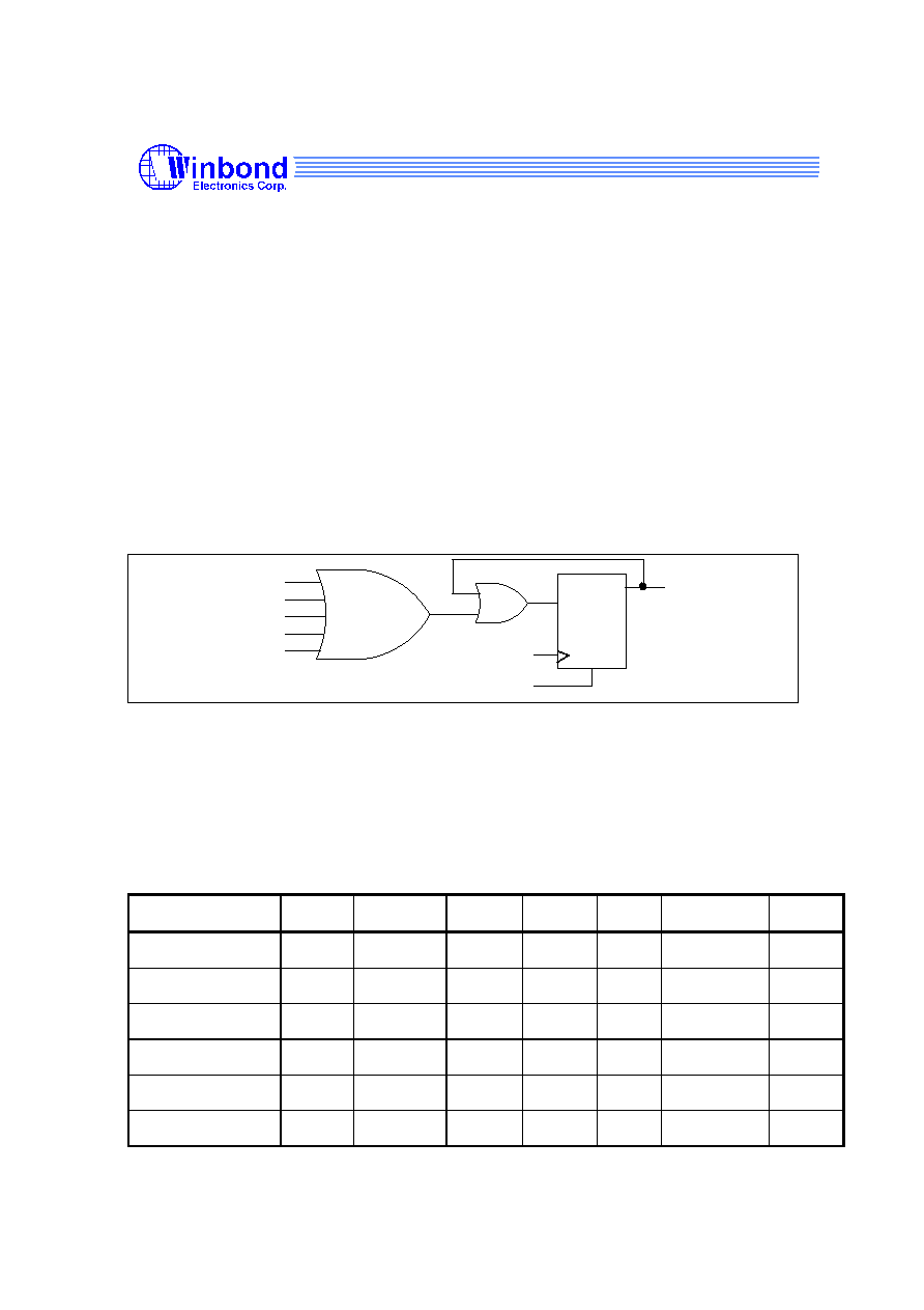
W925E/C240
8-bit CID Microcontroller
-36-
Release Date : 2002/7/2
Revision : A6
The Watchdog timer can be used as a system monitor or a simple timer. In either case, when the
time-out count is reached, the Watchdog timer interrupt flag WDIF (WDCON.3) is set. If the
enable bit EIE.5 enables the interrupt, then an interrupt will occur.
The Serial block can generate interrupts on reception or transmission. There are one interrupt
sources from the Serial block, which are obtained by SF1 in the SCON1. SF1 is cleared
automatically when the serial port interrupt is serviced.
The divider interrupt is generated by DIVF that is set when divider overflows. DIVF is set by
hardware and cleared when divider interrupt is serviced. The divider interrupt is enable/disable if
the bit EDIV is high/low.
The comparator interrupt is produced by COMPF, which is set when the RESC bit is changed
from low to high. RESC, which is the real-time result of comparator, is set when the voltage of
reference input is higher than the voltage of analog input.
The CID interrupt is generated by CIDF. The CIDF is a logic OR output of all CID flags which are
set by hardware and cleared by software. The structure of the CID flags is shown in Figure 6-4.
Each of the individual interrupts can be enabled or disabled by setting or clearing the
corresponding bits in the IE and EIE SFR. A bit EA, which is located in IE.7, is a global control bit
to enable/disable the all interrupt. When bit EA is zero all interrupts are disable and when bit EA
is high each interrupt is enable individually by the corresponding bit.
RNGF
FDRF
ALGOF
DTMFDF
CIDF
R
System clock
Clear by software
D
FSF
Figure 6-4 The Structure of CID Flags
Priority Level Structure
There are two priority levels for the interrupts, high and low. The interrupt sources can be
individually set to either high or low levels. Naturally, a higher priority interrupt cannot be
interrupted by a lower priority interrupt. However there exists a pre-defined hierarchy amongst the
interrupts themselves. This hierarchy comes into play when the interrupt controller has to resolve
simultaneous requests having the same priority level. This hierarchy is defined as shown below;
the interrupts are numbered starting from the highest priority to the lowest.
Table 4 Interrupt table.
Interrupt
Flag
Name
Flag
Location
EN Bit
EN Bit
Location
Priority Flag Cleared
by
Interrupt
Vector
External interrupt 0 IE0
TCON.1
EX0
IE.0
1
(higest)
hardware +
software
03h
Timer0 overflow
TF0
TCON.5
ET0
IE.1
2
hardware +
software
0Bh
External interrupt 1 IE1
TCON.3
EX1
IE.2
3
hardware +
software
13h
Timer1 overflow
TF1
TCON.7
ET1
IE.3
4
hardware +
software
1Bh
Serial port
SF1
SCON1.7 ES1
IE.6
5
hardware +
software
3Bh
External interrupt 2
IE2
EXIF.0
EX2
EIE.0
6
hardware +
software
43h
W925E/C240
8-bit CID Microcontroller
-37-
Release Date : 2002/7/2
Revision : A6
External interrupt 3
IE3
EXIF.1
EX3
EIE.1
7
hardware +
software
4Bh
CID
CIDF
EXIF.2
ECID
EIE.2
8
software
53h
Divider overflow
DIVF
EXIF.3
EDIV
EIE.3
9
hardware +
software
5Bh
Compare difference
COMPF EXIF.4
ECOMP EIE.4
10
hardware +
software
63h
Watchdog timer
WDIF
WDCON.3 EWDI
EIE.5
11
(lowest)
software
6Bh
Ps: The flags marked as the italic font are not bit-addressable.
The interrupt flags are sampled every machine cycle. In the same machine cycle, the sampled
interrupts are polled and their priority is resolved. If certain conditions are met then the hardware
will execute an internally generated LCALL instruction which will vector the process to the
appropriate interrupt vector address. The conditions for generating the LCALL are
1. An interrupt of equal or higher priority is not currently being serviced.
2. The current polling cycle is the last machine cycle of the instruction currently being executed.
3. The current instruction does not involve a write to IP, IE, EIP or EIE registers and is not a RETI.
If any of these conditions is not met, then the LCALL will not be generated. The polling cycle is
repeated every machine cycle, with the interrupts being sampled in the same machine cycle. If an
interrupt flag is active in one cycle but not responded to, and is not active when the above
conditions are met, the denied interrupt will not be serviced. This means that active interrupts are
not remembered. Note that every polling cycle is new.
Execution continues from the vectored address until an RETI instruction is executed. On
execution of the RETI instruction, the processor pops out the top content of Stack to the PC. The
processor is not notified anything if the content of stack was changed. Note that a RET instruction
would perform exactly the same process as a RETI instruction, but it would not inform the
Interrupt Controller that the interrupt service routine is completed, and would leave the controller
still thinking that the service routine is underway.
6.8 Programmable Timers/Counters
The W925E/C240 has 2 16-bit timer/counters. There are two 8-bit registers to perform a 16-bit
counting register in every timer/counter. In timer/counter 0, TH0 is the upper 8 bits register and
TL0 is the lower 8 bits register. Similarly timer/counter 1 have two 8-bit registers, TH1 and TL1.
Each timer/counter has 4 kind of clock sources which are Fosc/4, Fosc/64, Fosc/1024 and Fs.
There are 3 operating modes in each timer/counter 0 and 1. The operating modes of timer/
counter0 is identical to timer/counter1. The overflow signal of each timer/counter is sampled at
phase 2 in every system machine cycle, therefore when the system clock and the timer/counter
clock both are from sub-oscillator, if the overflow frequency is higher than Fs/4 the overflow flag
can not be sampled correctly. Only one overflow flag can be sampled in a machine cycle others
will be missed.
MODE 0
In Mode 0, the timer/counters act as 13-bit timer/counters. The 13 bits consist of 8 bits of THx and
lower 5 bits of TLx. The upper 3 bits of TLx are ignored.
The negative edge of the clock causes the content of the TLx register to increase one. When the
fifth bit in TLx moves from 1 to 0, then the count in the THx register is incremented. When the
count in THx moves from FFh to 00h, then the overflow flag TFx is set. The counted input is
enabled only if TRx is set and either GATE=0 or INTx =1. When C/ T is set to 0, then it will count
clock cycles, and if C/ T is set to 1, then it will count 1 to 0 transitions on T0 (P3.4) for timer 0 and
T1 (P3.5) for timer 1. When the 13-bit count reaches 1FFFh, the next count will cause it to rollover
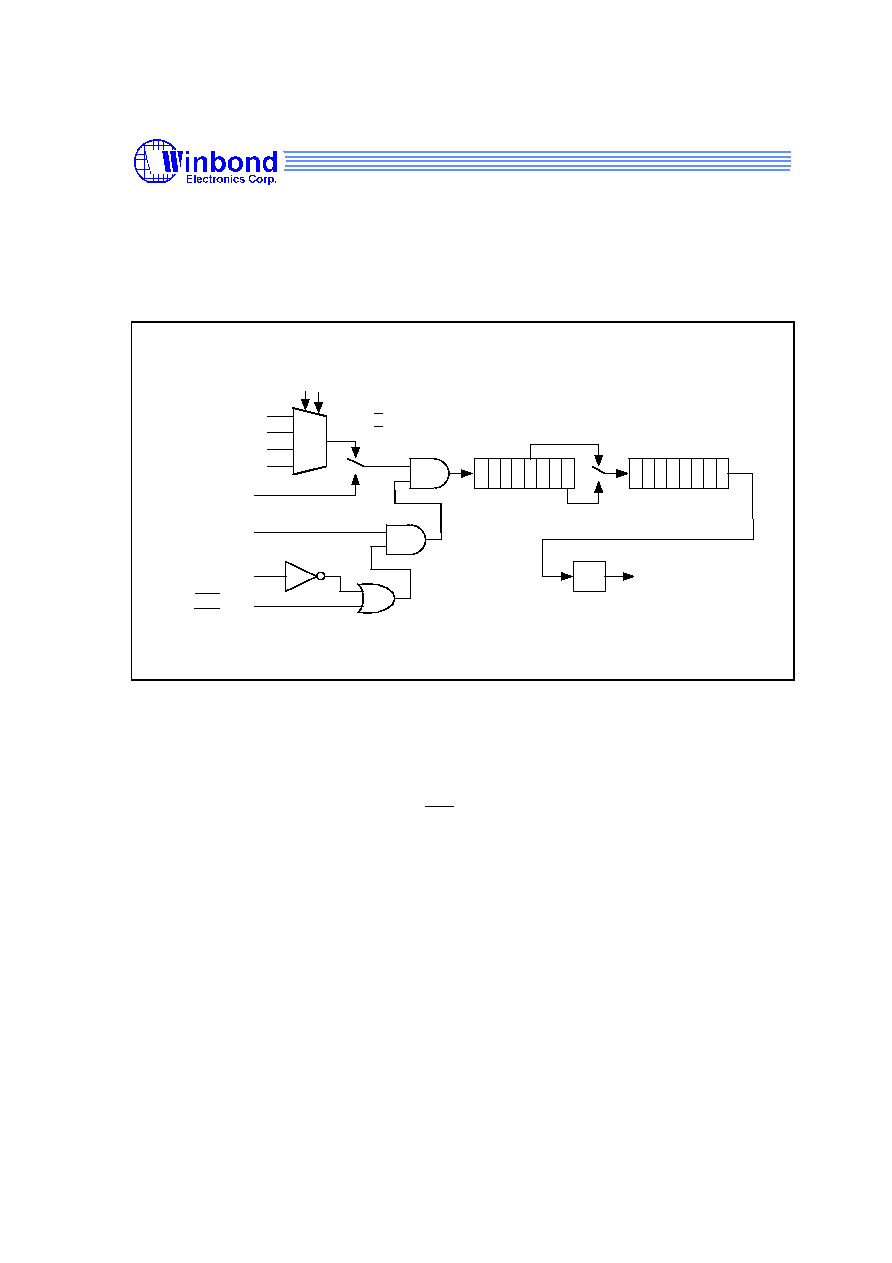
W925E/C240
8-bit CID Microcontroller
-38-
Release Date : 2002/7/2
Revision : A6
to 0000h. The timer overflow flag TFx of the relevant timer is set and if enabled an interrupts will
occur. Note that when they are used as a timer, the bits of the CKCON1 select the time-base.
MODE1
Mode 1 is similar to Mode 0 except that the counting register forms a 16-bit counter, rather than a
13 bit counter.
C/T = TMOD.2
(C/T = TMOD.6)
M1,M0 = TMOD.1,TMOD.0
(M1,M0 = TMOD.5,TMOD.4)
Interrupt
T0 = P3.4
(T1 = P3.5)
TH0
(TH1)
TL0
(TL1)
TF0
(TF1)
TR0 = TCON.4
(TR1 = TCON.6)
GATE = TMOD.3
(GATE = TMOD.7)
INT0 = P3.2
(INT1 = P3.3)
7
0
TFx
4
7
0
00
1
01
0
TM0=CKCON1.2, CKCON1.3
(TM1=CKCON1.4, CKCON1.5)
mux
00
01
10
11
PS: Functions of timer1 are shown in brackets
Fosc/4
Fosc/64
Fosc/1024
Fs
Figure 6-5 Mode 0 & Mode 1 of Timer/Counter 0 & 1
MODE 2
Mode 2 is the Auto Reload Mode. In mode 2, TLx acts as an 8-bit count register, while THx holds
the reload value. When the TLx register overflows from FFh to 00h, the TFx bit is set and TLx is
reloaded with the content of THx, and the counting process continues from the reloaded TLx. The
reload operation leaves the content of the THx register unchanged. Counting is controlled by the
TRx bit and the proper setting of GATE and INTx pins.
BUZZER
In mode 2, timer 0 can be use to output an arbitrary frequency to the BUZ pin by programming
bit6 and bit7 of CKCON2. BUZ pin can be configured as key tone (KT) output by setting BUZSL
to high. When disable buzzer output by clearing ENBUZ to low, the BUZ output is in floating
status.
In the case where timer 0 clock input is FT, the desired frequency for BUZ output = FT / (255 �
preset value + 1) / 2 (HZ).

W925E/C240
8-bit CID Microcontroller
-39-
Release Date : 2002/7/2
Revision : A6
C/T = TMOD.2
(C/T = TMOD.6)
Interrupt
T0 = P3.4
(T1 = P3.5)
TH0
(TH1)
TL0
(TL1)
TF0
(TF1)
TR0 = TCON.4
(TR1 = TCON.6)
GATE = TMOD.3
(GATE = TMOD.7)
INT0 = P3.2
(INT1 = P3.3)
7
0
TFx
7
0
PS: Functions of timer1 are shown in brackets
0
1
Fosc/4
Fosc/64
Fosc/1024
Fs
mux
TM0=CKCON1.2, CKCON1.3
(TM1=CKCON1.4, CKCON1.5)
1/2
KT
CKCON2.7
=ENBUZ
Pin BUZ
floating
Low
512Hz
1024Hz
2048Hz
mux
CKCON2.5, CKCON2.4
00
01
10
11
00
01
10
11
CKCON2.6
=BUZSL
FT
From
TM0
Figure 6-6 Mode 2 of Timer/Counter 0 & 1
When F
T
equals 32768 Hz, depending on the preset value of TM0, the BUZ pin will output a
single tone signal in the tone frequency range from 64 Hz to 16384 Hz. The relation between the
tone frequency and the preset value of TM0 is shown in the table below.
Table 5 The relation between the tone frequency and the preset value of TM0
C
C
#
B
G
F
E
D
A
#
#
D
#
#
G
F
A
E
N
O
T
TM0 preset value
& BUZ frequency
3rd octave
4th octave
5th octave
261.63
277.18
293.66
311.13
329.63
349.23
369.99
392.00
415.30
440.00
466.16
493.88
523.25
554.37
587.33
622.25
659.26
698.46
739.99
783.99
830.61
880.00
932.23
987.77
260.06
277.69
292.57
309.13
327.68
348.58
372.35
390.08
420.10
442.81
C1H
C5H
C8H
CBH
CEH
D1H
D4H
D6H
D9H
DDH
DBH
DF
H
468.11
496.48
E1H
E3H
E4H
E6H
E7H
E9H
EAH
EBH
ECH
EDH
EEH
EFH
528.51
564.96
585.14
630.15
655.36
712.34
744.72
780.19
819.20
862.84
910.22
963.76
130.81
138.59
146.83
155.56
164.81
174.61
185.00
196.00
207.65
220.00
233.08
246.94
83H
8AH
90H
97H
9DH
A2H
A7H
ACH
B1H
BAH
B6H
BEH
131.07
138.84
146.28
156.03
165.49
174.30
184.09
195.04
207.39
221.40
234.05
248.24
Tone
frequency
Tone
frequency
TM0 preset value
& BUZ frequency
Tone
frequency
TM0 preset value
& BUZ frequency
Note: Central tone is DB (440 Hz).
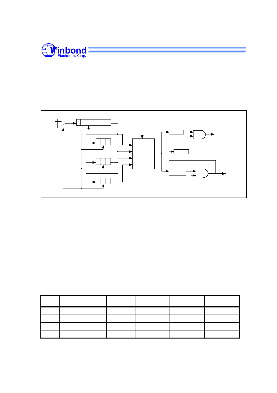
W925E/C240
8-bit CID Microcontroller
-40-
Release Date : 2002/7/2
Revision : A6
WATCHDOG TIMER
The Watchdog timer is a free-running timer that can be programmed by the user to serve as a
system monitor, a time-base generator or an event timer. It is basically a set of dividers that
divides the system clock. The divider output is selectable and determines the time-out interval. In
the condition of the timer-out expiring, the WDT interrupt and WDT reset may be executed if the
corresponding enable control bits are set. The interrupt will occur if the individual interrupt enable
and the global enable are set. The interrupt and reset functions are independent of each other
and may be used separately or together depending on the users software.
12
WD1,WD0
00
01
10
11
Interrupt
Reset
Enable Watchdog timer reset
EWT(WDCON.1)
Reset Watchdog
RWT (WDCON.0)
1
13
15
16
18
19
21
Time-out
selector
WDIF
WTRF
512 clock
delay
EWDI(EIE.5)
Fosc
Fsub
WFS(WDCON.4)
Figure 6-7 Watchdog Timer
The Watchdog timer should first be restarted by using RWT. This ensures that the timer starts
from a known state. The RWT bit is used to restart the watchdog timer. This bit is self clearing,
i.e. after writing a 1 to this bit the software will automatically clear it. The watchdog timer will now
count clock cycles. The time-out interval is selected by the two bits WD1 and WD0 (CKCON.7
and CKCON.6). When the selected time-out occurs, the Watchdog interrupt flag WDIF
(WDCON.3) is set. After the time-out has occurred, the watchdog timer waits for an additional 512
clock cycles. The software must issue a RWT to reset the watchdog before the 512 clocks have
elapsed. If the Watchdog Reset EWT (WDCON.1) is enabled, then 512 clocks after the time-out,
if there is no RWT, a system reset due to Watchdog timer will occur. This will last for two machine
cycles, and the Watchdog timer reset flag WTRF (WDCON.2) will be set. This indicates to the
software that the watchdog was the cause of the reset.
When used as a simple timer, the reset and interrupt functions are disabled. The timer will set the
WDIF flag each time the timer completes the selected time interval. The WDIF flag is polled to
detect a time-out and the RWT allows software to restart the timer. The Watchdog timer can also
be used as a very long timer. The interrupt feature is enabled in this case. Every time the time-out
occurs an interrupt will occur if the global interrupt enable EA is set.
Table 6 Time-out values for the Watchdog timer
WD1 WD0 Watchdog
Interval
Number of
Clocks
Fosc=
3.579545 MHz
Fosc=
32768 Hz
Reset of
Clocks
0
0
2
12
4096
1.14 mS
0.125 S
4608
0
1
2
15
32786
9.15 mS
1 S
33280
1
0
2
18
262144
73.23 mS
8 S
262656
1
1
2
21
2097152
585.87 mS
64 S
2097664

W925E/C240
8-bit CID Microcontroller
-41-
Release Date : 2002/7/2
Revision : A6
The Watchdog timer will de disabled by a power-on/fail reset. The Watchdog timer reset does not
disable the watchdog timer, but will restart it. In general, software should restart the timer to put it
into a known state.
The control bits that support the Watchdog timer are discussed below.
WATCHDOG CONTROL
WDIF: WDCON.3 - Watchdog Timer Interrupt flag. This bit is set whenever the time-out occurs in
the watchdog timer. If the Watchdog interrupt is enabled (EIE.5), then an interrupt will
occur (if the global interrupt enable is set and other interrupt requirements are met).
Software or any reset can clear this bit.
WTRF: WDCON.2 - Watchdog Timer Reset flag. This bit is set whenever a watchdog reset
occurs. This bit is useful for determined the cause of a reset. Software must read it, and
clear it manually. A Power-fail reset will clear this bit. If EWT = 0, then this bit will not be
affected by the watchdog timer.
EWT: WDCON.1 - Enable Watchdog timer Reset. This bit when set to 1 will enable the
Watchdog timer reset function. Setting this bit to 0 will disable the Watchdog timer reset
function, but will leave the timer running
RWT: WDCON.0 - Reset Watchdog Timer. This bit is used to clear the Watchdog timer and to
restart it. This bit is self-clearing, so after the software writes 1 to it the hardware will
automatically clear it. If the Watchdog timer reset is enabled, then the RWT has to be set
by the user within 512 clocks of the time-out. If this is not done then a Watchdog timer
reset will occur.
CLOCK CONTROL
WD1,WD0: CKCON.7, CKCON.6 - Watchdog Timer Mode select bits. These two bits select the
time-out interval for the watchdog timer. The reset time is longer 512 clocks time
than the interrupt time-out value.
The default Watchdog time-out is 2
12
clocks, which is the shortest time-out period. The EWT,
WDIF and RWT bits are protected by the Timed Access procedure. This prevents software from
accidentally enabling or disabling the watchdog timer. More importantly, it makes it highly
improbable that errant code can enable or disable the watchdog timer.
6.9 Serial Port 1
The P4.0 and P4.1 can be used as a 8-bit serial input/output port1. P4.0 is the serial port 1 clock
I/O pin and P4.1 is the serial port 1 data I/O pin. The serial port 1 is controlled by SCON1 register
which is described as below.
SF1: Serial port 1 interrupt flag. When 8-bits data is transceived completely, SF1 is set by
hardware. SF1 is cleared when serial interrupt1 routine is executed or cleared by software.
REN1: Set REN1 from 0 to 1 to start the serial port1 to receive 8-bit serial data.
SFQ: SFQ=0 Serial clock output frequency is equal to f
OSC
/2
SFQ=1 Serial clock output frequency is equal to f
OSC
/ 256
SEDG: SEDG=0 Serial data latched at falling edge of clock, SCLK=Low initially.
SEDG=1 Serial data latched at rising edge of clock, SCLK=High initially.
CLKIO: CLKIO=0 P4.0(SCLK) work as output mode
CLKIO=1 P4.0(SCLK) work as input mode
SIO: SIO=0 P4.0 & P4.1 work as normal I/O pin
SIO=1 P4.0 & P4.1 work as Serial port1 function
Any instruction causes a write to SBUF1 will start the transmission of serial port 1. As the REN1 is
from 0 to 1, the serial port 1 begins to receive a byte into SBUF1 in the frequency of the serial
clock. REN1 could be cleared by software after receive function begins. The LSB is transmitted/
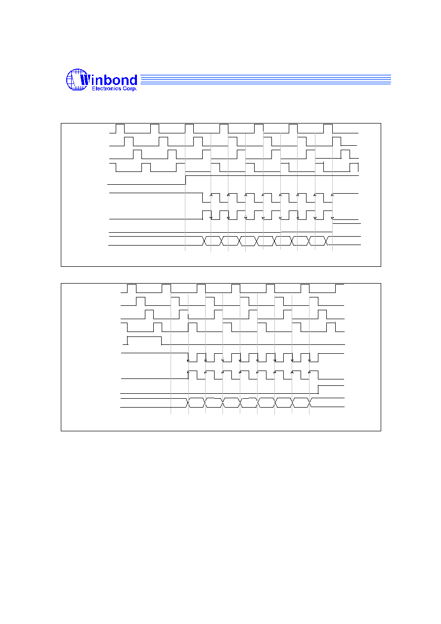
W925E/C240
8-bit CID Microcontroller
-42-
Release Date : 2002/7/2
Revision : A6
received first. The I/O mode of serial clock pin is controlled by CLKIO. User has to take care the
initial state of the serial port pins.
C1
C2
C3
C4
P4.0
SF1
REN1
P4.1
1
2
3
4
5
6
7
8
1
2
3
4
5
6
7
8
SEDG=1, rising latch
P4.0
SEDG=0, falling latch
NOTE: The serial clock frequency is fosc/2
Data Input
Figure 6-8 Timing of the Serial Port 1 Input Function
C1
C2
C3
C4
P4.0
Data output
SF1
Ins.
P4.1
1
2
3
4
5
6
7
8
1
2
3
4
5
6
7
8
SEDG=1, falling changed
P4.0
NOTE: The serial clock frequency is fosc/2
SEDG=0, rising changed
serial out
instruction
Figure 6-9 Timing of the Serial Port 1 Output Function
6.10 Comparator
A built-in comparator to compare the analog signal. There is a analog input paths from pin VNEG.
Two reference inputs, one is from pin VPOS and other is from regulator output. When the voltage
of positive input is higher than the negative input, the comparator output will be high. The
RESEC(COMPR.3) is the result of the comparison. An internal rising signal on RESC produces
interrupt flag of COMPF (EXIF.4). The flag COMPF is cleared when comparator interrupt routine
is executed or cleared by software. Set COMPEN to enable the comparator function.
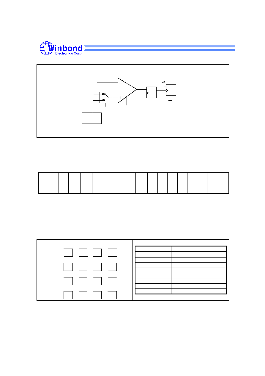
W925E/C240
8-bit CID Microcontroller
-43-
Release Date : 2002/7/2
Revision : A6
D
CK
C3
Clr
RESET
D
CK
RESC
Clr
COMPF=0
EXIF.4
(COMPF)
COMPEN
VNEG(P4.2)
VPOS(P4.4)
REF1
X.XV
REGULATOR
EN
SCON1.5(REGON)
REF
Figure 6-10 The Configuration of Comparator
The output voltage of the regulator is tunable by 4 bits in regulator voltage control register
(REGVC). When REGVC is equal to 0AH, the output voltage is 1.0V. The higher value of REGVC
the lower voltage output of regulator. The adjustable voltage range is about from 0.72V to 1.48V .
The variation of the voltage depends on the V
DD
. Following is the table of REGVC vs regulator
voltage.
Regvc
00
01
02
03
04
05 06
07
08 09
0ah 0bh 0ch 0dh 0eh 0fh
No
Loading(3V)
1.497
1.4464
1.3941
1.3426
1.2899
1.238
1.186
1.1352
1.081
1.029
0.976
0.924
0.869
0.815
0.762
0.7112
No
Loading(5V)
1.500
1.449 1.397 1.345 1.292 1.241
1.188
1.137 1.083
1.031
0.978
0.925
0.87 0.816
0.763
0.712
6.11 DTMF Generator
W925E/C240 provides a DTMF generator which outputs the dual tone multi-frequency signal to
the DTMF pin. The DTMF generator can work well at the operating frequency of 3.58MHz. A
DTMF generator register DTMFG controls the DTMF output and specifys the desired low/high
frequency. The tones are divided into two groups (low group and high group). When the
generator is disable, the DTMF pin is in tri-state. The relation between the DTMF signal and the
corresponding touch tone keypad is shown in Figure 6-11.
1
2
3
A
4
5
6
B
7
8
9
C
*
0
#
D
R1
R2
R3
R4
C1
C2
C3
C4
Row/Col
Frequency
R1
697 Hz
R2
770 Hz
R3
852 Hz
R4
941 Hz
C1
1209 Hz
C2
1336 Hz
C3
1477 Hz
C4
1633 Hz
Figure 6-11 The Relation Between DTMF and Keypad
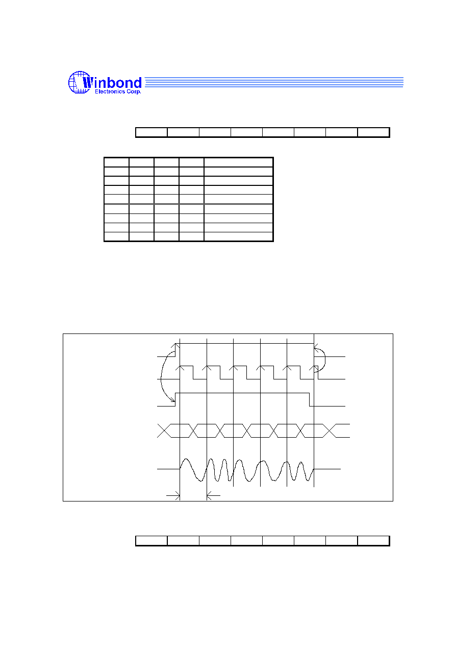
W925E/C240
8-bit CID Microcontroller
-44-
Release Date : 2002/7/2
Revision : A6
Bit:
7
6
5
4
3
2
1
0
-
DTGE
HE
LE
L1
L0
H1
H0
Mnemonic: DTMFG Address: BAh
L1
L0
H1
H0
Selected tone
x
x
0
0
1209Hz
x
x
0
1
1336Hz
x
x
1
0
1477Hz
x
x
1
1
1633Hz
0
0
x
x
697Hz
0
1
x
x
770Hz
1
0
x
x
852Hz
1
1
x
x
941Hz
LE: Enable low group frequency output.
HE: Enable high group frequency output.
DTGE: Enable dual tone output to DTMF pin.
6.12 FSK Generator
W925E/C240 provides a FSK generator which outputs the FSK signal to the DTMF pin. The FSK
output share with DTMF output pin. It can out FSK signal with 1200Hz baud rate of ITU-T V.23 or
Bellcore 202 signal. A FSK transmit data register (FSKTB) specifies the desired output data. The
FSK Transmit Control Register (FSKTC) can control whether the FSK signal will be output or not.
The relation timing is shown in Figure 6-12
Enable signal
(FTE)
Latch clock
Data latch Flag
Data
(FSKTB) bit0
(FDS)
FSK Signal
(DTMF pin)
1
0
1
1
0
0
Hi-Z
Hi-Z
Auto clear
Interrupt occur when rising edge
1
0
1
1
0
833us
[FSF]
Figure 6-12 FSK Modulator
FSK TRANSIMT CONTROL REGISTER (initial=00H)
Bit:
7
6
5
4
3
2
1
0
FTE
FTM
FDS
-
-
-
LO1
LO0
Mnemonic: FSKTC Address: C6h

W925E/C240
8-bit CID Microcontroller
-45-
Release Date : 2002/7/2
Revision : A6
FTE: FSK transmit Enable. Enable=1, Disable=0
FTM: FSK signal Standard. Bellcore 202=1, V.23=0
FDS: FSK data sending status
LO0, LO1: FSK transmit level option
FSK output level
LO1
LO0
150mV
0
0
120mV
0
1
95mV
1
0
75mV
1
1
FSK TRANSMIT DATA BUFFER
(initial=00H)
Bit:
7
6
5
4
3
2
1
0
FSKTB.7
FSKTB.6
FSKTB.5
FSKTB.4
FSKTB.3
FSKTB.2 FSKTB.1
FSKTB.0
Mnemonic: FSKTB Address: C7h
FSKTB.0:Only This bit will be latched and send out as FSK signal
When FTE enable will set the FDS to high to enable the internal latch clock in 1200Hz. When
FDS is in high state, FSKTB bit0 will be sent out by FSK modulator at the rising edge of latch
clock. FDS could be cleared by software to inform no more data will be sent out after the last bit is
sent completely. If the FDS is cleared then FTE will become low at next rising latch clock to
disable FSK modulator and clear FDS by hardware automatically.
When FTE is set, FSK modulation flag (FSF) will be set at every rising edge of latch clock to
produce an interrupt shared with CID interrupt routine. If a CID interrupt occurs, user can check
FSF to know if this interrupt is caused by FSK modulator. The only way to stop FSK signal
immediately is to disable FTE by software.
6.13 I/O Ports
There are five 8-bits ports named from P0 to P4 in W925E/C240. All ports can be configured as
input or output mode. Except P0, every port has pull high resistor enable/disable by PxH register.
After reset the initial state of each port is in input mode and the value of the registers from P0 to
P3 are FFh. The I/O port is described as below:
P0: I/O mode is controlled by P0IO. Only P0 output as open drain mode and without pull high
resistor.
P1: I/O mode is controlled by P1IO. Pull high is controlled by P1H. P1.0~P1.3 work as INT2,
P1.4~P1.7 work as INT3. Falling edge on P1 pins to produce INT2 and INT3 flag. P1 is
configured as INT2/INT3 by P1EF register.
P2: I/O mode is controlled by P2IO. Pull high is controlled by P2H.
P3: I/O mode is controlled by P3IO. Pull high is controlled by P3H.
P3.5
T1
Timer/counter 1 external count input
P3.4
T0
Timer/counter 0 external count input
P3.3
INT1
External interrupt 1
P3.2
INT0
External interrupt 0
P4: I/O mode is controlled by P4IO. Pull high is controlled by P4H.
Special function of P4 is described below.
P4.7-5
I/O
Normal I/O
P4.4
VPOS
Positive input of the comparator
P4.2
VNEG
Negative input of the comparator
P4.1
SDATA
Serial port output
P4.0
SCLK
Serial port input
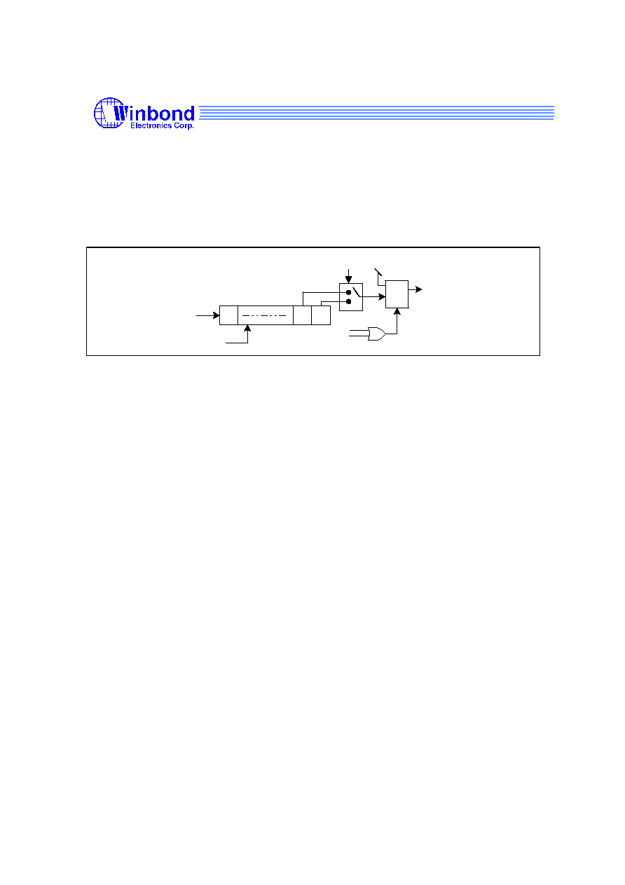
W925E/C240
8-bit CID Microcontroller
-46-
Release Date : 2002/7/2
Revision : A6
6.14 Divider
A built-in 13/14-bit binary up-counter designed to generate periodic interrupt. The clock source is
from sub-oscillator. When the frequency of sub-crystal is 32768Hz, it provides the divider interrupt
in the period of 0.25/0.5 second. Bit DIVS controls the degree of divider. When DIVA is high to
enable the divided counter, when DIVA is low to reset divider and stop counting. As the divider
overflows, the divider interrupt flag DIVF is set. DIVF is clear by software or serving divider
interrupt routine.
13 14
1
overflow
DIVF
(EXIF.3)
DIVS
(CKCON1.1)
DIVA
(DIVC.0)
Fs
ck
D
Q
CR
Executing DIV Int
Clear by software
Figure 6-13 13/14-bit Divider
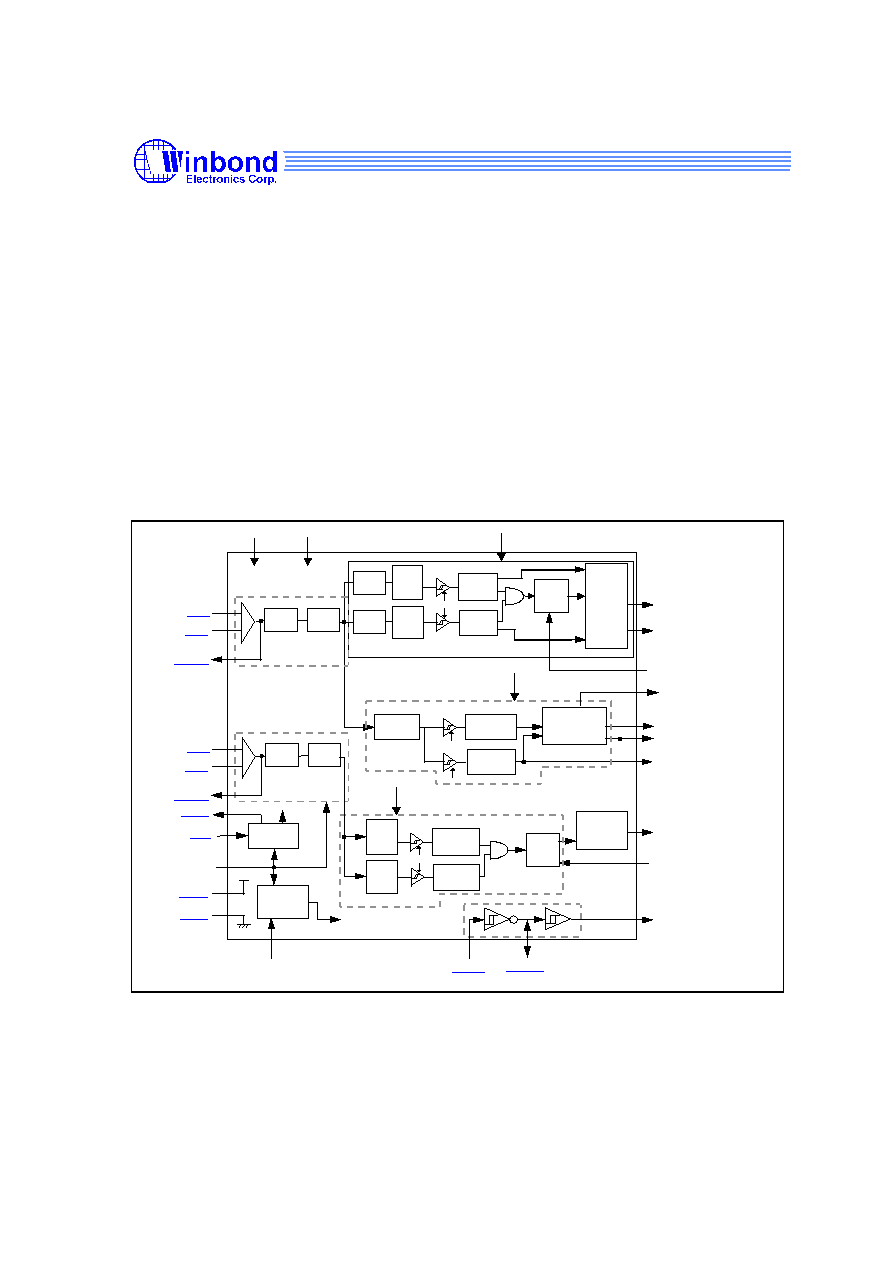
W925E/C240
8-bit CID Microcontroller
-47-
Release Date : 2002/7/2
Revision : A6
6.15 Calling Identity Delivery (CID)
W925E/C240 provides type I and type II of CID system. Type I is on-hook calling with CID
message and type II is off-hook call on waiting. The CID function includes FSK decoder, dual
tone alert signal detector, ring detector and DTMF receiver. The FSK demodulation function can
demodulate Bell 202 and ITU-T V.23 Frequency Shift keying (FSK) with 1200 baud rate. The
Tone Alert Signal detect function can detect dual tones of Bellcore Customer Premises
Equipment(CPE) Tone Alerting Signal(CAS) and BT Idle State and Loop State Tone Alert Signal.
The line reversal for BT, ring burst for CCA or ring signal for Bellcore can be detected by ring
detector. It is compatible with Bellcore TR-NWT-000030 & ST-TSV-002476, British Telecom(BT)
SIN227, U.K. Cable Communications Association(CCA) specification. The DTMF receiver can be
programmed as DTMF decoder to decode 16 DTMF signals or tone detector to detect the signal
which frequency is in DTMF band. The tone detector can be an auxiliary detector to improve the
performance of detecting tone alerting signal(CAS), said as talk down-off, in type II system.
The FSK decoder, alert tone detector and DTMF receiver can be enable/disable individually by
the bits of FSKE, CASE and DTMFE in FSK DATA REGISTER(FSKDR). CIDE is the global
control bit to enable/disable FSK decoder, alert tone detector and DTMF receiver. However, the
ring detector is always active.
FSK Bandpass
Filter
FSK
Demodulator
FSK
Data Output
Interface
FSK Carrier
Detector
Guard
Time
Circuit
Bias Voltage
Generator
To internal
circuit
Clock Driver
To internal
circuit
VREF
FCD
FDR
FD7-FD0
CIDE,RST
Fm
RNGDI
RNGRC
VADD
VASS
FSKE
FSK Demodulation Circuit
Dual Tone Alert Signal Detection Circuit
Ring Detector
Interrupt
Generator
INP1
INN1
GCFB1
ALGO
High Tone
Bandpass
Filter
Low Tone
Bandpass
Filter
Guard
Time
Timer
High Tone
Detector
Low Tone
Detector
Decode
data
and Latch
DTMFD
DD3-DD0
CASE
DTMFE
ESt
DTMFPT/DTMFAT
FDATA
INP2
INN2
+
-
Anti-alias
Filter
GCFB2
Input Pre-processor
CASPT/CASAT
RNG
CAP
PGAF
<3:0>
+
-
Anti-alias
Filter
Input Pre-processor
PGAF
<7:4>
PGD
<7:4>
PGD
<3:0>
PHAD<3:0>
PHFL<7:4>
High Tone
Bandpass
Filter
Low Tone
Bandpass
Filter
High Tone
Detector
Low Tone
Detector
PHAD<7:4>
PHFL<3:0>
CIDGD
CIDGA
PS: The signals noted in italic and underline type are CID pins on the chip.
Figure 6-14 The CID Block Diagram
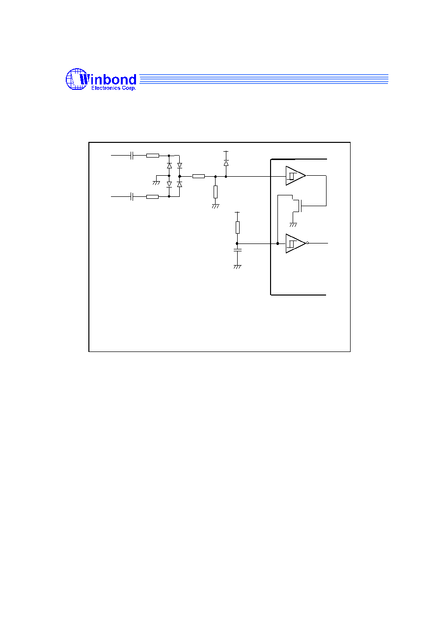
W925E/C240
8-bit CID Microcontroller
-48-
Release Date : 2002/7/2
Revision : A6
Ring Detector
The application circuit in Figure 6-15 illustrates the relationship between the RNGDI, RNGRC and
RNG signals. The combination of RNGDI and RNGRC is used to detect an increase of the
RNGDI voltage from ground to a level above the Schmitt trigger high going threshold voltage V
T+
.
Tip/A
R1=470K
C1=0.1uF
Ring/B
C1=0.1uF
C3=0.22uF
R5=150K
R2=470K
R3=200K
R4=300K
RNGDI
RNGRC
RNG
Allowance minimal ring voltage (peak to peak) is:
Vpp
(max ring)
= 2 (V
T+(max)
(R1 + R3 + R4) / R4 + 0.7)
Tolerance to noise between Tip and Ring and VSS is:
Vpeak
(max noise)
= V
T+(min)
(R1 + R3 + R4) / R4 + 0.7
Time constant is:
T = R5 C3 ln [VDD / (VDD - V
T+
)]
V
T+(min)
<= V
T+
<= V
T+(max)
R5 from 10K ohm to 500K ohm.
C3 from 47 nF to 0.68 uF.
Figure 6-15 Application Circuit of the Ring Detector
The RC time constant of the RNGRC pin is used to delayed the output pulse of the RNG flag for a
low going edge on RNGDI. This edge goes from above the V
T+
voltage to the Schmitt trigger low
going threshold voltage V
T-
. The RC time constant must be greater than the maximum period of
the ring signal, to ensures a minimum RNG high interval and to filter the ring signal to get an
envelope output. The rising signal of RNG will set the bit RNGF(CIDFG.0) high to cause the CID
flag(CIDF) high.
The diode bridge shown in Figure 6-15 works for both single ended ring signal and balanced
ringing. The R1 and R2 are used to set the maximum loading and must be of equal value to
achieve balanced loading at both the tip and ring line. R1, R3 and R4 form a resistor divider to
supply a reduced voltage to the RNGDI input. The attenuation value is determined by the
detection of minimal ring voltage and maximum noise tolerance between tip/ring and ground.
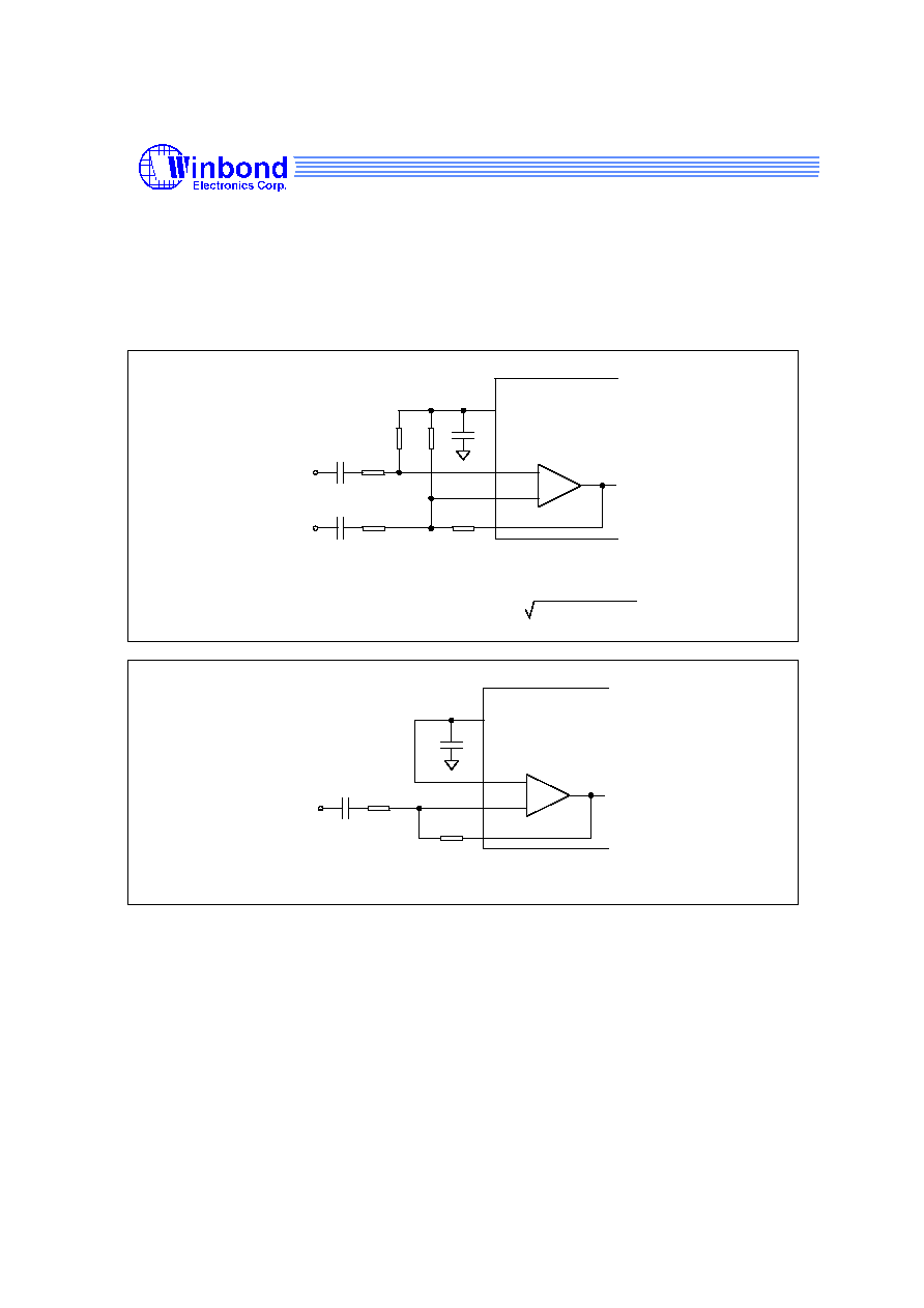
W925E/C240
8-bit CID Microcontroller
-49-
Release Date : 2002/7/2
Revision : A6
Input Pre-Processor
The input signal is processed by Input Pre-Processor, which is comprised of two OP amps and a
bias source(VREF). The gain OP-amps are used to bias the input voltage with the VREF signal
voltage. VREF is V
AD
/2 typically, this pin is recommended to connect a 0.1 uF capacitor to V
AS
.
The gain adjustable OP amps are sued to select the input gain by connecting a feedback resistor
between GCFB and INN pins. Figure 6-16 shows the differential input configuration and Figure
6-17 shows the single-ended configuration.
+
-
INP
INN
VREF
C1
C2
R1
R2
R3
R4
0.1uF
R5
Differential Input Amplifier
C1 = C2
R1 = R2
R3 = (R4 R5) / (R4 + R5)
Voltage Gain
Av = R5 / R1
Input Impedance
Zin = 2 R1 + (1 / wC)
2
2
GCFB
Figure 6-16 Differential Input Gain Control Circuit
+
-
INP
INN
VREF
C
R1
0.1uF
R2
Voltage Gain
Av = R2 / R1
GCFB
22n
Figure 6-17 Single-Ended Input Gain Control Circuit
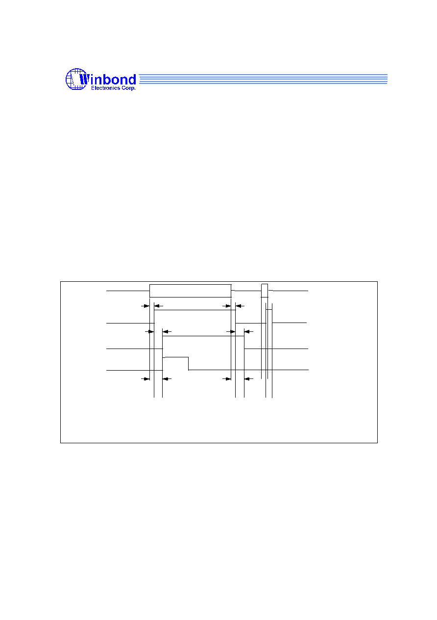
W925E/C240
8-bit CID Microcontroller
-50-
Release Date : 2002/7/2
Revision : A6
CAS/DTAS Detection
In off-hook services (type II), the detection of CAS/DTAS will affect the quality of the call waiting
service. When the CAS/DTAS is sent from far end, sometimes the near end user maybe still
talking. The CPE must be able to detect the CAS/DTAS successfully in the presence of near end
speech. To detect CAS/DTAS from telephone hybrid receiver pair improves the detection.
However in BT' s on-hook CID system the CAS/DTAS detection is from Tip/Ring pair.
The dual tone alert signal is separated into high and low tones and detected by a high/low tone
detector. When the alert tone is recognized by the detector, the bit ALGO will go high and the
rising signal will set the bit ALGOF in CIDFG to produce the CID flag(CIDF). Figure 6-18 shows
the guard time waveform of detecting alert tone. The total recognition time is t
REC
=t
DP
+t
GP
, where
t
DP
is the tone present detect time and t
GP
is the tone present guard time. The total absent guard
time is t
ABS
=t
DA
+t
GA
where t
DA
is the tone absent detect time and t
GA
is the tone absent guard time.
The tone present/absent guard time is determined by guard-time timer which the input clock
period is 0.858mS. When the alert tone is detected the internal signal ALGR will be set and the
rising edge of ALGR resets the guard-time timer and the timer starts up counting from 00H. As
the content of the timer is the same as the register CASPT, the timer stops counting and the bit
ALGO will be set and the rising edge of ALGO triggers the flag ALGOF to become high. The
counting of tone absent time is similar to the counting of tone present time but the falling edge of
ALGR/ ALGO replaces the rising edge and the CASAT replaces the CASPT. The bit ALGO is
controlled by hardware only. The flag ALGOF is set by rising edge of ALGO and cleared by
software.
ALGR
Vin
Dual Alert Tone Signal
t
DP
t
GP
t
DA
t
GA
*
1: Guard time timer is reset and starts to up count from 00H.
2: Guard time timer is reset and starts to up count from 00H.
3: The content of the guard-time timer reaches the content of ASPT/ASAT.
t
REC
t
ABS
1
2
3
3
*ALGR is an internal signal in the uC.
+ Clear by software.
ALGO
ALGOF
+
1
t
DP
t
DA
Figure 6-18 Guard Time Waveform of Alert Tone Signal Detection
DTMF Decoder
The DTMF decoder shares the same input pre-processor with FSK decoder. The dual tone is
separated into low group and high group by two SCFs (switched capacitor filter. The method of
DTMF detection is the same as alert tone detection. The present/absent guard time is adjusted by
registers DTMFPT/DTMFAT. As the DTMF signal is recognized and decoded, the bit DTMFD will
be set and the decoded DTMF data is stored in bit0 to bit3 of register DTMFDR. The rising edge
of DTMFD produces the flag DTMFDF. The bit DTMFD is controlled by hardware only. The flag
DTMFDF is set by rising edge of DTMFD and cleared by software.
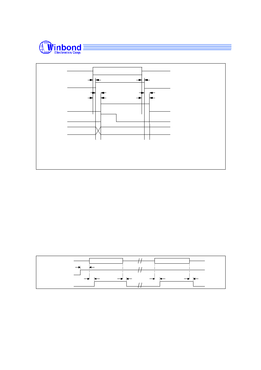
W925E/C240
8-bit CID Microcontroller
-51-
Release Date : 2002/7/2
Revision : A6
ESt
Vin (Tip/ring)
TONE #n
t
DP
t
GP
t
REC
t
DA
t
GA
t
ABS
DTMFD
*
1
2
3
3
DTMFDR
Tone #n-1
Tone #n
* ESt is an internal signal in the circuit.
+ Clear by software.
1: Guard time timer is reset and starts to up count from 00H.
2: Guard time timer is reset and starts to up count from 00H.
3: The content of the up counting timer reaches the register DTMFPT/DTMFAT.
DTMFDF
+
Figure 6-19 The Waveform of DTMF Detection
Tone Detector
In off-hook state, said type II system, detecting tone alert signal(CAS) is easily interfered by
human' s voice or other noise in voice band. Sometimes the interference makes falsely
recognizing a noise as a CAS(talk-off), or lost detecting a real CAS(talk-down). The DTMF can be
programmed as a tone detector by setting bit 4 of DTMFR2. The frequency band of the tone
detector is DTMF frequency from 697Hz to 1633Hz. Once the tone detector gets signals in the
band, the bit of DTMFH or DTMFL in register DTMFDR will become high immediately. User can
poll these 2 bits to check if the tone exists on the tip/ring. The input gain of tone detector is the
same as DTMF receiver.
FSK Decoder
The FSK carrier detector provides an indication of the present of a signal within the FSK
frequency band. If the output amplitude of the FSK band-pass filter is sufficient to be detected
continuously for 8 mS, the FSK carrier detected bit FCD will go high and it will be released if the
FSK band-pass filter output amplitude is not able to be detected for greater than 8 mS. The 8 mS
is the hysteresis of the FSK carrier detector. Figure 6-20 shows the timing of FSK carrier
detection.
Tip/Ring
FCD
Analog FSK Signal
t
CP
t
CA
FSKE
t
FSKE
Analog FSK Signal
t
CP
t
CA
Note
Figure 6-20 FSK Detection Enable and FSK Carrier Present and Absent Timing
The FSK demodulation function can demodulate Bell 202 and ITU-T V.23 Frequency Shift keying
(FSK) with 1200 baud rate. When the decoder receives the FSK serial data, the serial data will be
demodulated into bit FDATA with 1200 baud rate in the mean time the synchronous clock signal
is output to the bit FCLK. As the decoder receives one byte, the internal serial-to-parallel circuit
sets the bit FDR and converts the 8-bit serial data into the byte register FSKDR. The rising edge
of bit FDR will set the flag FDRF to produce CID interrupt but FDRF is cleared by software. User
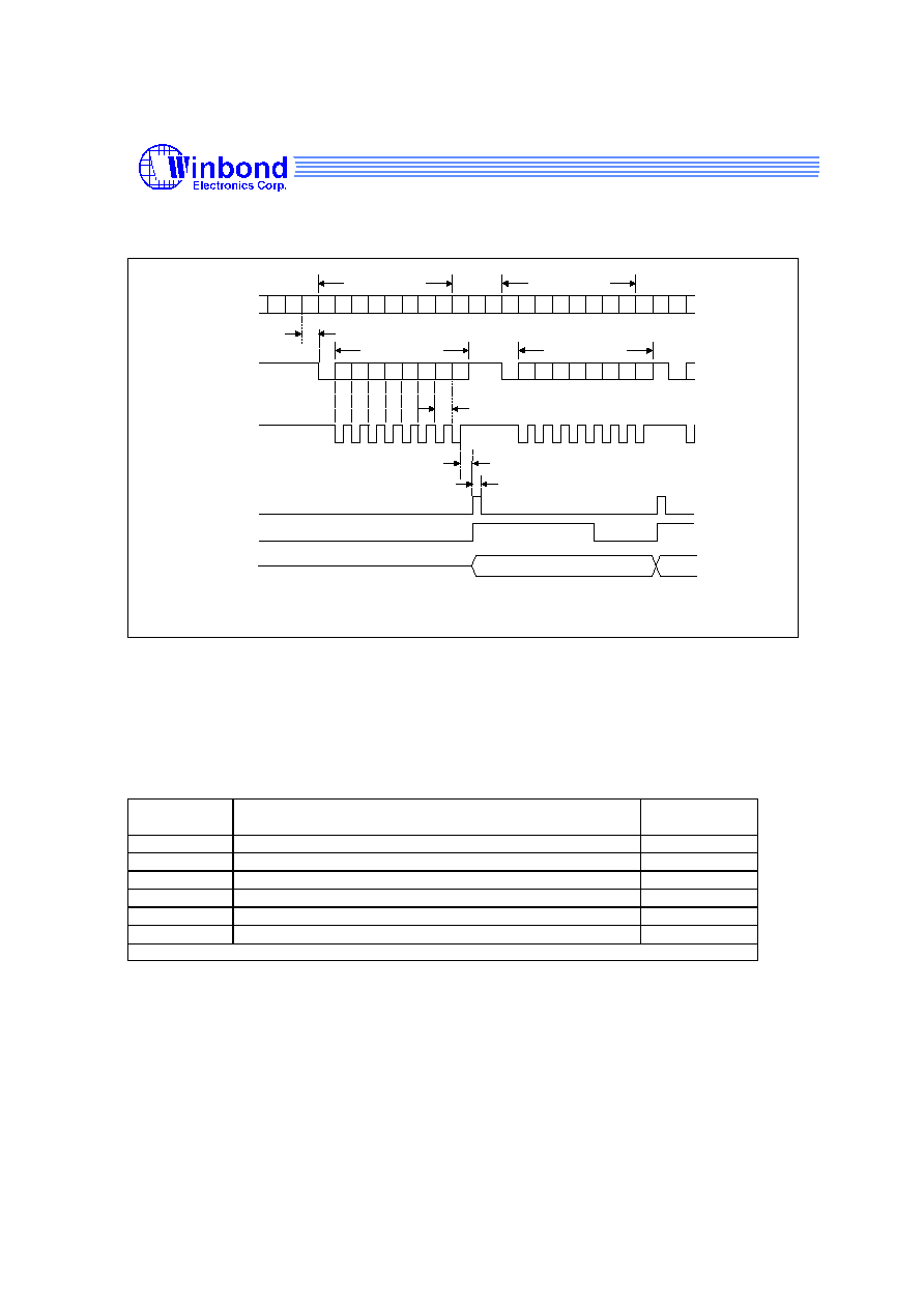
W925E/C240
8-bit CID Microcontroller
-52-
Release Date : 2002/7/2
Revision : A6
can get the FSK data by reading register FSKDR or sampling the bit FDATA. The timing of FSK
demodulation is shown in Figure 6-21.
Tip/Ring
1*
1
0
b0
b1
b2
start
b3
b4
b5 b6
b7 1*
0
b0
b1 b2
b3
b4 b5
b6 b7
1
1
0
b0
stop
start
stop
start
FDATA
b0
b1 b2
b3
b4 b5
b6 b7
b0 b1
b2
b3 b4
b5 b6
b7
start
stop
start
stop
start
t
IDD
FCLK
FDR
1/f
DCLK0
t
CRD
t
RH
1st byte data
2nd byte data
1st byte data
2nd byte data
* Mark bit or redundant stop bit(s), will be omitted.
+ Clear by software.
FDRF
+
FSKDR
1st byte data
2nd byte data
Figure 6-21 Serial Data Interface Timing of FSK Demodulation
CID Input Gain Control
The CID input gain and input hysteresis are controllable by internal CID gain control registers.
CIDGD and CIDGA registers determine the 6 internal CID gain control registers. CID gain control
data register (CIDGD) presents the data bus. The lower 3 bits of CID gain control address register
(CIDGA) presents the address. The rising edge of CIDGA.4 will latch the CIDGD in the
corresponding internal CID gain control register. The 6 internal CID gain control registers are
addressed as following table. Setting the 6 registers as the suggestion value guarantees the CID
spec.
Address
(CIDGA.2-0)
Internal CID Gain Control Register
Suggestion
Value
000
DTMFR1: DTMF register1
0000 0001B
001
DTMFR2: DTMF register2
011X 0001B
�
002
PGAF: Programmable gain control alert tone and FSK
99H
003
PGAD: Programmable gain control DTMF
A7H
004
PHAD: Programmable hysteresis alert tone and DTMF
35H
005
PHFL: Programmable hysteresis FSK and low pass filter 33H
�
X=0 DTMF receiver works a DTMF decoder, X=1 DTMF receiver works as a tone detector.
The signals to set internal CID gain control registers is shown in Figure 6-22
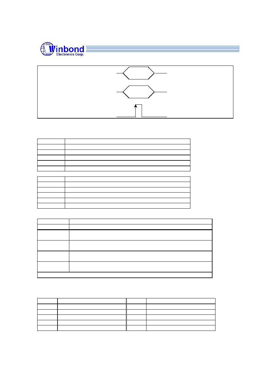
W925E/C240
8-bit CID Microcontroller
-53-
Release Date : 2002/7/2
Revision : A6
CIDGD
CIDGA<2:0>
CIDGA.3
CIDGD
CIDGA
Rising latch
Figure 6-22 Internal CID Gain Control Register Setting Waveform
DTMFR1
DTMFR1[7:4] are reserved bits and must be 0000b.
Bit3~Bit0 Acceptable error percentage to sample 4 period of Row freq.
0000
0.6% (default)
0001
2.5%
001X
3.5%
01XX
Reserved
1XXX
Reserved
DTMFR2
Bit3~Bit0 Acceptable error percentage to sample 4 period of Col freq.
0000
0.5% (default)
0001
1.5%
001X
2.5%
01XX
Reserved
1XXX
Reserved
The acceptable error percentage may have small variation by different test environments.
DTMFR2.4=0 DTMF receiver works as a DTMF receiver
DTMFR2.4=1 DTMF receiver works as a tone detector
DTMFR2.5=0 DTMF PT counter is up counter type, detected frequency changed
does not effect counter
DTMFR2.5=1 DTMF PT counter is up counter type, detected frequency changed
resets DTMF PT counter
DTMFR2.6=0 DTMF AT counter is up-down counter type, up counting when no
DTMF detected, down counting if DTMF detected again.
DTMFR2.6=1 DTMF AT counter is up counter type, up counting when no DTMF
detected, pause counting if DTMF detected again.
DTMFR2.7: reserved
There are 4 programmable gain arrays, shown in Figure 6-14, are determined by Low/High
nibbles of PGxx. The following table lists the input gain corresponding to the value of L/H nibble
of PGxx.
X
20 log((40+15*X)/(230-(40+15*X))) dB
X
20 log((40+15*X)/(230-(40+15*X))) dB
0
-13.53
6
2.28
1
-10.05
7
4.64
2
-7.18
8
7.18
3
-4.64
9
10.05
4
-2.28
10
13.53

W925E/C240
8-bit CID Microcontroller
-54-
Release Date : 2002/7/2
Revision : A6
5
0.00
X is the value of L/H nibble of PGxx
There are 4 programmable hysteresis input buffer, shown in Figure 6-14, are determined by Low/
High nibbles of PHxx. The hysteresis control formulas are list below.
Alert tone hysteresis
HAT=13mv + 3mv*X
X=PHAD<7:4>
DTMF hysteresis
HDTMF=6mv + 3mv*X
X=PHAD<3:0>
FSK hysteresis
HFSK=13mv + 3mv*X
X=PHFL<7:4>
FSK detector hysteresis
HFSKD=13mv + 3mv*X
X=PHFL<3:0>
Application Circuit
The analog interface circuit of W925E/C240 shown in Figure 6-23 is a typical CPE system. The
gain control op-amp is set to unit gain to allow the electrical characteristics to be met in this
application circuit.
34K
34K
430K
430K
22nF
22nF
53K6
60K4
464K
INP2
INN2
GCFB2
VREF
CAP
RNGDI
RNGRC
INP1
0.1uF
470K
470K
0.1uF
0.1uF
200K
100K
150K
Tip/A
Ring/B
INN1
GCFB1
464K
464K
464K
60K4
60K4
464K
Speech
Network
Speaker
Microphone
Tx+
Tx-
Rx+
Rx-
Tip
Ring
Resistor must have 1% tolerance
Resistor must have 5% tolerance
0.47u
22nF
22nF
Figure 6-23 Application Circuit of CID

W925E/C240
8-bit CID Microcontroller
-55-
Release Date : 2002/7/2
Revision : A6
Application Environment
There are three major timing differences for CID sequences, Bellcore, BT and CCA. Figure 6-24
is the timing diagram for Bellcore on-hook data transmission and Figure 6-25 is the timing
diagram for the Bellcore off-hook data transmission. Figure 6-26 is the timing diagram for the BT
caller display service on-hook data transmission and Figure 6-27 is the timing diagram for the BT
caller display service off-hook data transmission. Figure 6-28 is the timing diagram for the CCA
caller display service for on-hook data transmission. The CID flag (CIDF) must be cleared by
software when each time the CID interrupt routine is serviced. The CID global enable signal
(CIDE) must be set high.
Tip/Ring
RNG
FSKE
FCD
FDR
FCLK
FDATA
1st Ring
Ch. seizure
Mark
Message
2nd Ring
A
...
...101010...
B
C
D
E
F
Data
...
CIDF
...
...
A = 2 sec typical
B = 250-500mS
C = 250mS
D = 150mS
E = depend on data length
MAX C+D+E = 2.9 TO 3.7 sec
F >= 200mS
Figure 6-24 Input and Output Timing of Bellcore On-hook Data Transmission
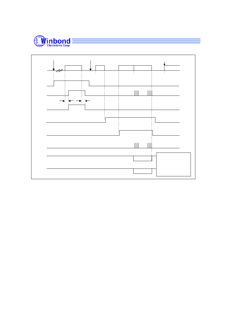
W925E/C240
8-bit CID Microcontroller
-56-
Release Date : 2002/7/2
Revision : A6
Tip/Ring
FSKE
FCD
FDR
FCLK
FDATA
ALGO
CPE unmutes handset and
enable keypad
G
CAS
t
REC
t
ABS
A
B
ACK
C
CPE goes off-hook
D
E
F
Mark
Message
CPE sends
CPE mutes handset & disables keypad
...
Data
CIDF
...
A = 75 - 85mS
B = 0 - 100mS
C = 55 - 65mS
D = 0 - 500mS
E = 58 - 75mS
F = depends on data length
G <= 50mS
ASE
Figure 6-25 Input and Output Timing of Bellcore Off-hook Data Transmission
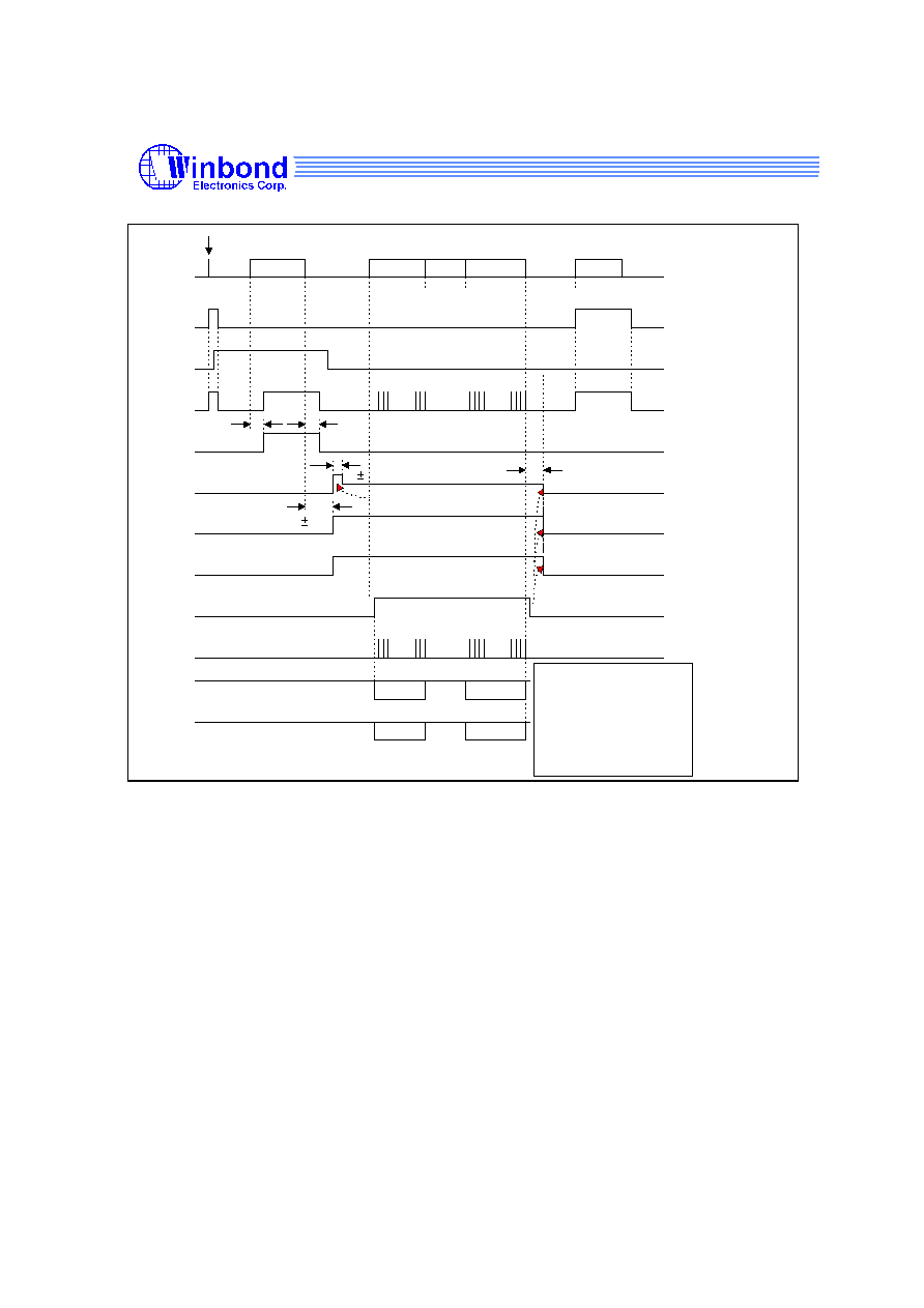
W925E/C240
8-bit CID Microcontroller
-57-
Release Date : 2002/7/2
Revision : A6
A/B Wires
RNGON
ASE
ALGO
TE DC load
TE AC load
FSKE
FCDN
FDRN
DCLK
DATA
Line Reversal
Alert Signal
Ch. Seizure
Mark
Message
Ring
t REC
t ABS
15
1 ms
20
5 ms
A
B
C
D
E
F
G
...
...
...101010...
Data
Note 1
50 - 150 ms
Note 2
Note 3
< 120uA
Zss (Refer to SIN227)
Current wetting pulse (Refer to SIN227)
CIDF
...
...
< 0.5 mA (optiona)
A >= 100mS
B = 88 - 100mS
C >= 45mS (up to 5Sec)
D = 80 - 262mS
E = 45 - 75mS
F <= 2.5S (500mS typical)
G >= 200mS
Figure 6-26 Input and Output Timing of BT Idle State (On-hook) Data Transmission
Note:
1. SIN227 specifies that the AC and DC loads should be applied at 20
�
5mS after the end of the dual tone alert
signal.
2. SIN227 specifies that the AC and DC loads should be removed between 50 � 150mS after the end of the FSK
signal.
3.
The FSKE bit should be set low to disable the FSK decoder when FSK is not expected. The tone alerting signal
speech and the DTMF tones are in the same frequency band as the FSK signal.

W925E/C240
8-bit CID Microcontroller
-58-
Release Date : 2002/7/2
Revision : A6
Tip/Ring
FSKE
FCD
FDR
FCLK
FDATA
ALGO
CPE unmutes handset and
enable keypad
H
CAS
t
REC
t
ABS
B
C
ACK
D
CPE goes off-hook
E
F
G
Mark
Message
CPE sends
CPE mutes handset & disables keypad
...
Data
CIDF
...
A = 40 - 50mS
B = 80 - 85mS
C <= 100mS
D = 65 - 75mS
E = 5 - 100mS
F = 40 - 75mS
G = depends on data length
H <= 100mS
ASE
Start Point
A
Note 1
Note 3
Note 2
Note 4
Note 5
Figure 6-27 Input and Output Timing of BT Loop State (Off-hook) Data Transmission
Note:
1. In a CPE where AC power is not available, the designer may choose to switch over to line power when the CPE
goes off-hook and use battery power while on-hook.
2. The FSKE bit may be set low to prevent the alert tone, speech or other FSK in-band noise decoded by FSK
demodulator and give false data when the dual tone alert signal is expected. If the FSKE pin can not controlled by
micro-controller, the FSKE bit must always placed in high state and the micro controller must give up the FSK
decoded data when the FSK signal is not expected.
3. The exchange will have already disabled the speech path to the distant customer in both transmission directions.
4. The FSKE should be set high as soon as the CPE has finished sending the acknowledge signal ACK.
5. The FSKE may be set low after the last byte (check sum) has been decoded or FCD has become inactive.
6. In an unsuccessful attempts where the exchange does not send the FSK signal, the CPE should disable FSKE,
un-mute the handset and enable the keypad after this interval.

W925E/C240
8-bit CID Microcontroller
-59-
Release Date : 2002/7/2
Revision : A6
A/B Wires
RNG
CIDE
TE DC load
TE AC load
FSKE
FCD
FDR
FCLK
FDATA
Line Reversal
Ring Burst
Ch. Seizure
Mark
Message
First Ring Cycle
A
B
C
D
E
F
...
...
...101010...
Data
Note 2
Note 3
Note 4
CIDF
...
...
250 - 400 ms
50 - 150 ms
Note 1
A = 200 - 450mS
B >= 500mS
C = 80 - 262mS
D = 45 - 262mS
E <= 2.5sec (500ms typical)
F >= 200mS
Figure 6-28 Input and Output Timing of CCA Caller Display Service Data Transmission
Notes:
1. The CPE designer may choose to set FSKE always high while the CPE is on-hook and the FSK signal is
expected.
2. TW/P & E/312 specifies that the AC and DC loads should be applied between 250 - 400 mS after the end of the
ring burst.
3. TW/P & E/312 specifies that the AC and DC loads should be removed between 50 - 150 ms after the end of the
FSK signal.
4. The CID may not be enable up at the first ring cycle after the FSK data had been processed.
W925E/C240
8-bit CID Microcontroller
-60-
Release Date : 2002/7/2
Revision : A6
7 ELECTRICAL CHARACTERISTICS
7.1 Maximum Ratings*
(Voltage referenced to VSS pin)
Parameter
Symbol Rating
Units
1 Supply Voltage with respect to VSS
V
DD
-0.3 to 6
V
2 Voltage on any pin other than supplies (note 1)
-0.7 to VDD + 0.7 V
3 Current at any pin other than supplies
0 to 10
MA
4 Storage Temperature
Tst
-65 to 150
� J
Note:
*. Exposure to conditions beyond those listed under Absolute Maximum Ratings may adversely affect the lift and reliability
of the device.
1. VDD + 0.7 should not excess maximum rating of supply voltage.
7.2
Recommended Operating Conditions
Characteristics
Symbol Rating
Unit
Power Supplies (Analog)
V
AD
3.0 to 6.0
V
Power Supplies (Digital)
V
DD
2.2 to 6.0
V
Main Clock Frequency
f
OSC
3.579545
MHz
Sub Clock Frequency
f
SUB
32768
Hz
Tolerance on Clock Frequency
f
C
-0.1 to +0.1
%
Operation Temperature
T
op
0 to 75
�
C
7.3 DC Electrical Characteristics
Parameter
Symbol Condition
Min
Typ
Max Unit Note
Operating Current
I
OP1
FSK On, dual
clock, normal
run
2.8
mA
I
OP2
FSK Off, dual
clock, normal
run
1.3
mA
I
OP3
FSK off, slow
run, main osc
stopped
50
uA
I
OP4
Idle mode,
dual clock
500
uA
I
OP5
Idle mode,
main osc
stopped
50
uA
I
OP6
Power down
mode
1
uA
I/O Ports Input High
Voltage
V
IH
0.7V
DD
V
DD
V
I/O Ports Input Low
Voltage
V
IL
V
SS
0.3V
DD
V
I/O Ports Output High
Voltage
V
OH
I
OH
= 2.0mA
2.4
-
-
V
I/O Ports Output Low
Voltage
V
OL
I
OL
= 2.0mA
-
-
0.4
V
W925E/C240
8-bit CID Microcontroller
-61-
Release Date : 2002/7/2
Revision : A6
BUZ Pin Output High
Voltage
V
BOH
I
OH
= 3.5mA
2.4
-
-
V
BUZ Pin Output High
Voltage
V
BOL
I
OL
= 3.5mA
0.4
-
-
V
DTMF Output DC
Level
V
TDC
R
L
= 5K
,
V
DD
= 2.5-3.8
1.1
-
2.8
V
DTMF Distortion
DTHD
R
L
= 5K
,
V
DD
= 2.5-3.8
-
-30
-23
dB
DTMF Output Voltage V
TO
Low group,
R
L
= 5K
130
150
170
mV
rms
Pre-emphasis
Col/Row
1
2
3
dB
FSK Output DC
Level
V
FDC
R
L
= 5K
,
V
DD
= 2.5-3.8
1.1
-
2.8
V
FSK Distortion
FTHD
R
L
= 5K
,
V
DD
= 2.5-3.8
-
-
-30
dB
FSK Output Voltage
V
FD
R
L
= 5K
75
150
170
mV
rms
Port Pull High Resistor R
PH
100
360
1000 K
Schmitt Input High
Threshold
V
T+
RNGDI,
RNGRC
0.48V
AD
-
0.68V
AD
V
Schmitt Input High
Threshold
V
T-
RNGDI,
RNGRC
0.28V
AD
-
0.48V
AD
V
Schmitt Hysteresis
V
HYS
RNGDI,
RNGRC
0.2
V
RNGRC Low Sink
Current
I
RNGL
RNGRC
2.5
mA
Input Current
I
IN
INPx, INNx,
RNGDI
-
-
1
�
A
Reference Output
voltage
V
REF
VREF
0.5V
AD
�
4%
-
0.5V
AD
+
4%
V No load
Reference Output
Resistance
R
REF
VREF
-
-
2
K
W925E/C240
8-bit CID Microcontroller
-62-
Release Date : 2002/7/2
Revision : A6
7.4 Electrical Characteristics - Gain Control OP-Amplifier
(Electrical characteristics supersede the recommended operating conditions unless otherwise stated.)
Parameter
Symbol Min Typ
Max Units Test Conditions
Input Leakage Current
I
IN
1
�
A
V
SS
V
IN
V
DD
Input Resistance
R
IN
10
M
Input Offset Voltage
V
OS
25 mV
Power Supply Rejection Ratio
PSRR 40
dB
1 kHz 0.1 Vpp ripple on V
DD
Maximum Capacitive Load (GCFBx)
C
L
100
pF
Maximum Resistive Load (GCFBx) R
L
50
k
Note: "
" Typical figure are at V
DD
= 5V and temperature = 25
� J
are design aids only, not guaranteed and not subject to
production testing.
7.5 AC Electrical Characteristics
(AC timing characteristics supersede the recommended operating conditions unless otherwise stated.)
Dual Tone Alert Signal Detection Interface
Parameter
Symbol Min
Typ
Max
Units Notes
Low Tone Frequency
f
L
2130
Hz
High Tone Frequency
f
H
2750
Hz
Frequency Deviation accept
1.1
%
3
Frequency Deviation reject
3.5
%
4
Maximum Input Signal Level
0.22
dBm
a
Input Sensitivity per tone
-40
-38
dBm 5
Reject Signal Level per tone
-48
dBm 5
Positive and negative twist
b
accept
7
dB
Noise Tolerance
SNR
TONE
20
dB
1, 2
Notes:
a. dBm = decibels with a reference power of 1 mW into 600 ohms, 0 dBm = 0.7746 Vrms.
b. Twist = 20 log (fH amplitude / fL amplitude).
1. Both tones have the same amplitude. Both tones are at the nominal frequencies.
2. Band limited random noise
300 - 3400 Hz. Present only when tone is present.
3. Range within which tones are accepted.
4. Ranges outside of which tones are rejected.
5. These characteristics are at V
DD
= 5V and temperature = 25
� J
.
Dual Tone Alert Signal Detection
Parameter
Condition Symbol Min
Typ
Max Units Notes
Alert Signal present detect time
t
DP
0.5
10
MS
Alert Signal absent detect time
ALGR
t
DA
0.1
8
MS
"
" Typical figure are at V
DD
= 5V and temperature = 25
� J
are design aids only, not guaranteed and not subject to
production testing.
W925E/C240
8-bit CID Microcontroller
-63-
Release Date : 2002/7/2
Revision : A6
FSK Detection Interface
Parameter
Symbol Min
Typ
Max
Units
Notes
Input Frequency Detection
Bell 202 Mark (logic 1)
Bell 202 Space (logic 0)
ITU-T V.23 Mark (logic 1)
ITU-T V.23 Space (logic 0)
f
Mark
f
Space
f
Mark
f
Space
1188
2178
1280.5
2068.5
1200
2200
1300
2100
1212
2222
1319.5
2131.5
Hz
+/- 1 %
+/- 1 %
+/- 1.5 %
+/- 1.5 %
Maximum Input Signal Level
-5.78
dBm
Input Sensitivity
-43
dBm 1, 3
Transmission Rate
1188
1200
1212
baud
Input Noise Tolerance
SNR
TONE
20
dB 1, 2
Notes:
1. Both mark and space have the same amplitude. Both mark and space are at the nominal frequencies.
2. Band limited random noise 300 - 3400 Hz. Present only when FSK signal is present.
3. These characteristics are at VDD = 5V and temperature = 25
� J
.
FSK Detection
Parameter
Condition Symbol Min
Typ
Max Units Notes
FSK detection enable time
FSKE
t
FSK
25
MS
Input FSK to FCD high delay
t
CP
25
MS
Input FSK to FCD low delay
FCD
t
CA
8
MS
Data Ready ACK Time
FDR
t
DR
415
416
417
US 2
Rate
1188
1200
1212 BpS 1
Input FSK to DATA delay
DATA
t
IDD
1
5
MS
Frequency
f
DCLK
1201.6 1202.8 1204
Hz 2
High Time
t
CH
415
416
417
US 2
Low Time
DCLK
t
CL
415
416
417
US 2
DCLK to FDR delay
DCLK, FDR t
CRD
415
416
417
US 2
Note :
1. FSK input data rate at 1200 +/- 12 baud.
2. OSCI frequency at 3.579545 MHz +/- 0.1%.
"
" Typical figure are at V
DD
= 5V and temperature = 25
� J
are design aids only, not guaranteed and not subject to
production testing.
DTMF Decoder
Parameter
Symbol Min
Typ
Max
Units Notes
Input Sensitivity per tone
-29
1
dBm 1,2
Positive and negative twist
accept
7
dB 1,2
Frequency Deviation accept
1.5
% 1,2
Frequency Deviation reject
3.5
% 1,2
3rd Tone Tolerance
-16
dB 1,2,3
Noise Tolerance
-12
dB 1,2,3
Dial tone Tolerance
22
dB 1,2,4
Note :
1. signal consists of all DTMF tones.
2. Tone duration is 40mS at least, tone pause duration is 40mS at least.
3. Referenced to the lowest level frequency component in DTMF signal.
4. Referenced to the minimum valid accept level.

W925E/C240
8-bit CID Microcontroller
-64-
Release Date : 2002/7/2
Revision : A6
DTMF Detection Interface
Parameter
Condition Symbol Min
Typ
Max Units Notes
DTMF present detect time
t
FP
0.5
8
MS
DTMF absent detect time
Est
t
FA
0.1
8
MS
DTMF Detected Duration
DTMFD=1
t
DD
40
MS
DTMF Signal Ignore Time
DTMFD=0
t
DI
20
MS
DTMF Pause Accept Time
DTMFD=1
t
DPA
20
MS
"
" Typical figure are at V
DD
= 5V and temperature = 25
� J
are design aids only, not guaranteed and not subject to
production testing.
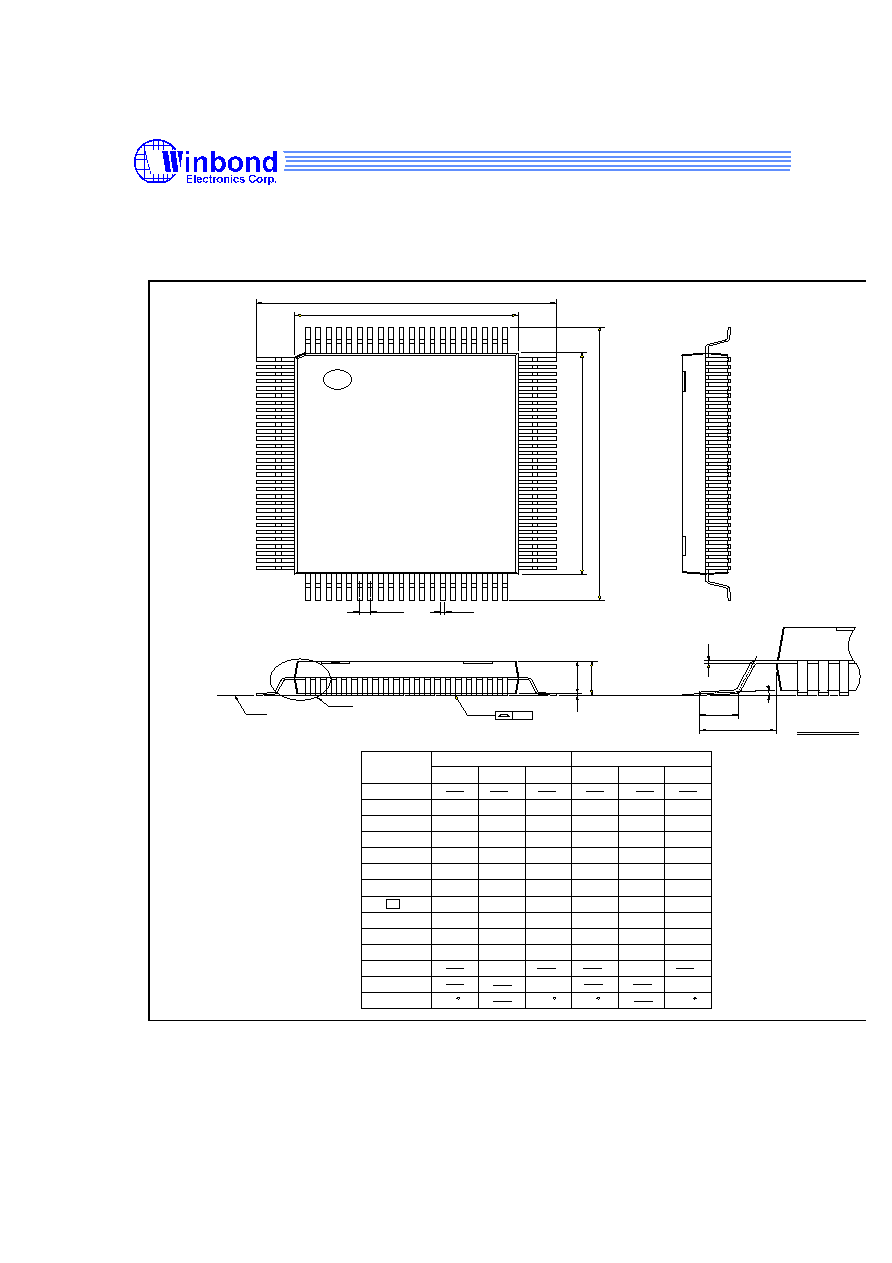
W925E/C240
8-bit CID Microcontroller
-65-
Release Date : 2002/7/2
Revision : A6
8 PACKAGE
100L QFP(14x20x2.75mm footprint 4.8mm)
E
H
y
A
A2
Seating Plane
L
L
1
See Detail F
0.08
0
7
0
0.003
2.40
1.40
19.20
1.20
18.80
1.00
18.40
0.064
0.055
0.992
0.756
0.047
0.976
0.740
0.039
0.960
0.746
0.65
20.10
14.10
0.20
0.40
2.87
20.00
14.00
2.72
19.90
13.90
0.10
0.20
2.57
0.791
0.555
0.008
0.016
0.113
0.787
0.551
0.107
0.026
0.783
0.547
0.004
0.008
0.101
Symbol
Min
Nom
Max
Max
Nom
Min
Dimension in inch
Dimension in mm
A
b
c
D
e
H
D
H
E
L
y
A
A
L
1
1
2
E
0.012
0.006
0.15
0.30
24.40
24.80
25.20
7
0.020
0.032
0.498
0.802
0.35
0.25
0.010
0.014
0.018
0.45
Controlling dimension : Millimeters
A1
E
D
H
D
e
b
c

W925E/C240
8-bit CID Microcontroller
-66-
Release Date : 2002/7/2
Revision : A6
9 VERSION STATEMENT
Version Modification
A6
1. Add initial state of registers
2. Modify description of WDCON.0